SYSMAC CPM1/CPM1A/CPM2A/CPM2C/SRM1(–V2). Programmable Controllers (2001) - page 8
Communications Instructions
Section
7-30
Application Example
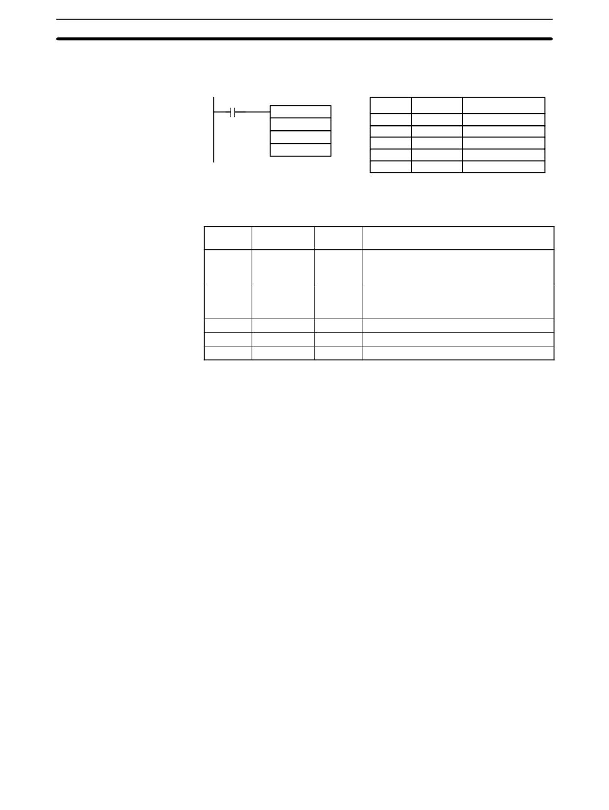
This example shows a program that transfers the contents of DM 0100 through
DM 0104 to the PC Setup area for the built-in RS-232C port (DM 6645 through
DM 6649).
00000
Address
Instruction
Operands
@STUP(--)
00000
LD
00000
000
00001
@STUP(--)
DM 0100
000
000
DM
0100
---
The settings are transferred as shown below. The Changing RS-232C Setup
Flag (SR 25312) will be turned OFF when the transfer has been completed.
The following table shows the function of the transferred setup data.
Source
Destination
Content
Function
word
word
DM 0100
DM 6645
1001
Enables the communications settings in DM
0101 and sets the communications mode to
no-protocol.
DM 0101
DM 6646
0803
Sets the following communications settings:
9,600 bps, 1 start bit, 8-bit data, 1 stop bit,
no parity
DM 0102
DM 6647
0000
No transmission delay (0 ms)
DM 0103
DM 6648
2000
Enables the end code CR, LF.
DM 0104
DM 6649
0000
(No function when DM 6648 is set to 2000.)
Flags
ER:
Indirectly addressed DM word is non-existent. (Content of DM word is
not BCD, or the DM area boundary has been exceeded.)
The port specifier (N) isn’t 000.
In the CPM2A/CPM2C, the Communications Switch on the front of the
CPU Unit is ON.
Another STUP(--) instruction is already being executed or event proc-
essing is being performed.
The specified source words exceed the data area.
The instruction was executed from an interrupt program.
The PC Setup is write-protected.
506
SECTION 8
PC Operations and Processing Time
This section explains the internal processing of the CPM1, CPM1A, CPM2A, CPM2C, and SRM1(-V2), as well as the time
required for processing and execution. Refer to this section to gain an understanding of the precise timing of PC operation.
8-1
CPM1/CPM1A Cycle Time and I/O Response Time
508
8-1-1
The CPM1/CPM1A Cycle
508
8-1-2
CPM1/CPM1A Cycle Time
509
8-1-3
I/O Response Time
510
8-1-4
One-to-one PC Link I/O Response Time
511
8-1-5
Interrupt Processing Time
513
8-1-6
CPM1/CPM1A Instruction Execution Times
514
8-2
CPM2A/CPM2C Cycle Time and I/O Response Time
519
8-2-1
CPM2A/CPM2C Cycle Time
519
8-2-2
I/O Response Time
520
8-2-3
One-to-one PC Link I/O Response Time
521
8-2-4
Interrupt Processing Time
523
8-2-5
CPM2A/CPM2C Instruction Execution Times
524
8-3
SRM1(-V2) Cycle Time and I/O Response Time
533
8-3-1
The SRM1(-V2) Cycle
533
8-3-2
SRM1(-V2) Cycle Time
534
8-3-3
I/O Response Time
536
8-3-4
One-to-one PC Link I/O Response Time
537
8-3-5
Interrupt Processing Time
538
8-3-6
SRM1(-V2) Instruction Execution Times
539
507
CPM1/CPM1A Cycle Time and I/O Response Time
Section
8-1
8-1
CPM1/CPM1A Cycle Time and I/O Response Time
8-1-1
The CPM1/CPM1A Cycle
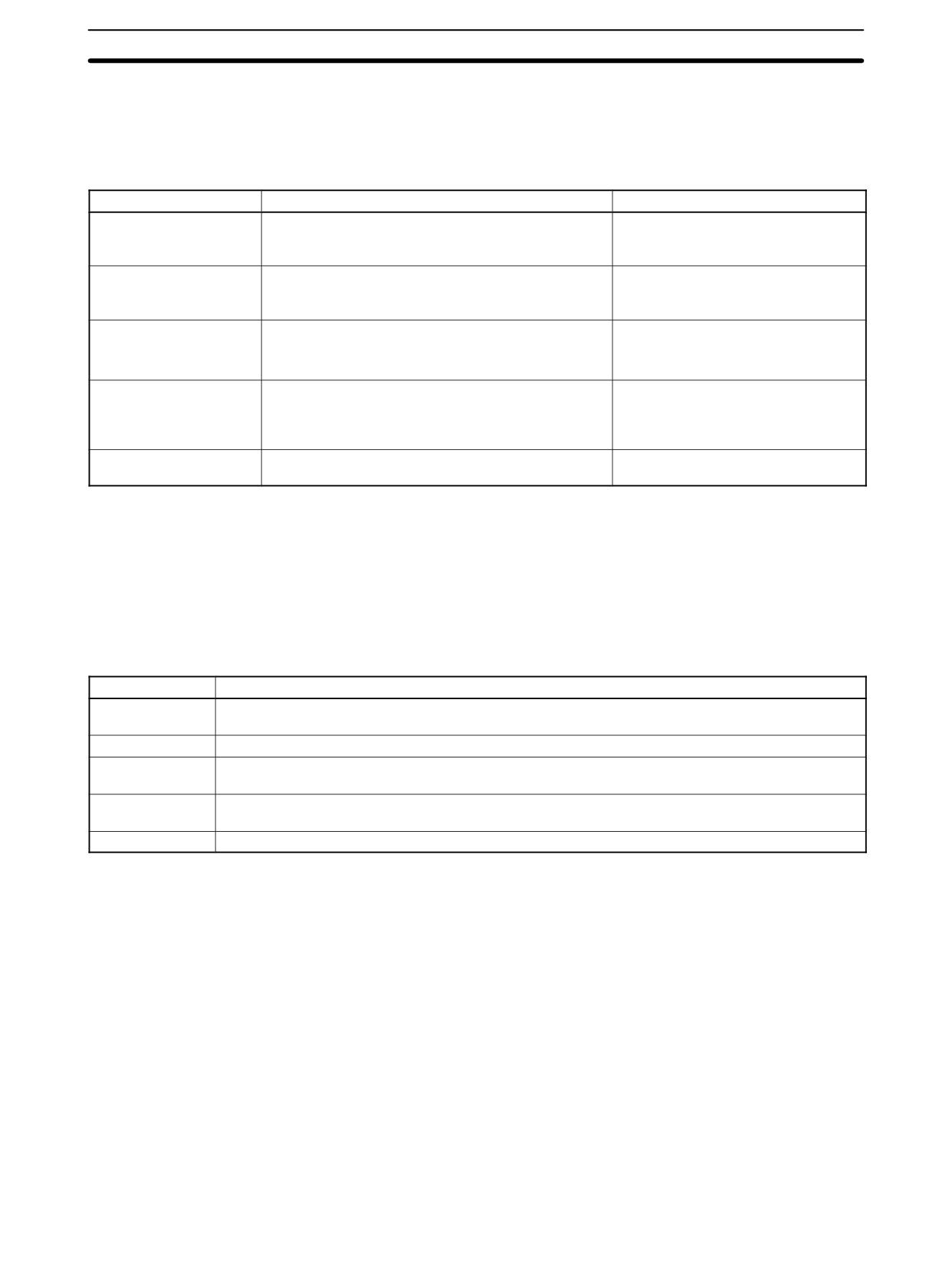
The overall flow of CPM1/CPM1A operation is as shown in the following flow-
chart.
Power application
Initialization processes
Initialization
Check hardware and
Program Memory.
No
Check OK?
Overseeing
processes
Yes
Set error flags and
Preset cycle time
activate indicators.
monitoring time.
ALARM
(flashing)
Execute user program.
ERROR or ALARM?
No
Program
End of program?
ERROR
execution
(lit)
Yes
Check cycle time setting.
Cycle
Minimum
No
time
cycle time set?
Cycle time
Yes
processing
Wait until minimum cycle
time expires.
Compute cycle time.
Refresh input bits and
output terminals.
I/O refreshing
Service peripheral port.
Service
peripheral
port.
Note Initialization processes include clearing the IR, SR, and AR areas, presetting
system timers, and checking I/O Units.
508
CPM1/CPM1A Cycle Time and I/O Response Time
Section
8-1
8-1-2
CPM1/CPM1A Cycle Time
The processes involved in a single CPM1/CPM1A cycle are shown in the follow-
ing table, and their respective processing times are explained.
Process
Content
Time requirements
Overseeing
Setting cycle watchdog timer, I/O bus check, UM
0.6 ms
check, clock refreshing, refreshing bits allocated to
new functions, etc.
Program execution
User program is executed.
Total time for executing instructions.
(Varies according to content of user’s
program.)
Cycle time calculation
Standby until set time, when minimum cycle time is
Almost instantaneous, except for
set in DM 6619 of PC Setup.
standby processing.
Calculation of cycle time.
I/O refresh
Input information is read to input bits.
10-point CPU :
0.06 ms
Output information (results of executing program) is
20-point CPU:
0.06 ms
written to output bits.
30-point CPU:
0.3 ms
Expansion I/O Unit:
0.3 ms
Peripheral port servicing
Devices connected to peripheral port serviced.
0.26 ms min., 5% or less of cycle
time up to 66 ms (see note)
Note The percentage of the cycle allocated to peripheral port servicing can be
changed in the PC Setup (DM 6617).
Cycle Time and Operations
The effects of the cycle time on CPM1/CPM1A operations are as shown below.
When a long cycle time is affecting operation, either reduce the cycle time or im-
prove responsiveness with interrupt programs.
Cycle time
Operation conditions
10 ms or longer
TIMH(15) may be inaccurate when TC 004 through TC 127 are used (operation will be normal for
TC 000 through TC 003).
20 ms or longer
Programming using the 0.02-second Clock Bit (SR 25401) may be inaccurate.
100 ms or longer
TIM may be inaccurate. Programming using the 0.1-second Clock Bit (SR 25500) may be inaccu-
rate. A CYCLE TIME OVER error is generated (SR 25309 will turn ON). See note 1.
120 ms or longer
The FALS 9F monitoring time SV is exceeded. A system error (FALS 9F) is generated, and opera-
tion stops. See note 2.
200 ms or longer
Programming using the 0.2-second Clock Bit (SR 25501) may be inaccurate.
Note
1. The PC Setup (DM 6655) can be used to disable detection of CYCLE TIME
OVER error.
2. The cycle monitoring time can be changed in the PC Setup (DM 6618).
Cycle Time Example
In this example, the cycle time is calculated for a CPM1/CPM1A CPU Unit with
20 I/O points (12 input points and 8 output points). The I/O is configured as fol-
lows:
Inputs: 1 word (00000 to 00011)
Outputs: 1 word (01000 to 01007)
The rest of the operating conditions are assumed to be as follows:
User’s program:500 instructions (consists of only LD and OUT)
Cycle time:
Variable (no minimum set)
509
CPM1/CPM1A Cycle Time and I/O Response Time
Section
8-1
The average processing time for a single instruction in the user’s program is as-
sumed to be 2.86 µs. The cycle times are as shown in the following table.
Process
Calculation method
Time with Programming De-
Time without Programming
vice
Device
1. Overseeing
Fixed
0.6 ms
0.6 ms
2. Program execution
2.86 × 500 (µs)
1.43 ms
1.43 ms
3. Cycle time calculation
Negligible
0 ms
0 ms
4. I/O refresh
0.01 × 1 + 0.005 × 1 (µs)
0.06 ms
0.06 ms
5. Peripheral port servicing
Minimum time
0.26 ms
0 ms
Cycle time
(1) + (2) + (3) + (4) + (5)
2.35 ms
2.09 ms
Note
1. The cycle time can be read from the PC via a Programming Device.
2. The maximum and current cycle time are stored in AR 14 and AR 15.
3. The cycle time can vary with actual operating conditions and will not neces-
sarily agree precisely with the calculated value.
8-1-3
I/O Response Time
The I/O response time is the time it takes after an input signal has been received
(i.e., after an input bit has turned ON) for the PC to check and process the in-
formation and to output a control signal (i.e., to output the result of the proces-
sing to an output bit). The I/O response time varies according to the timing and
processing conditions.
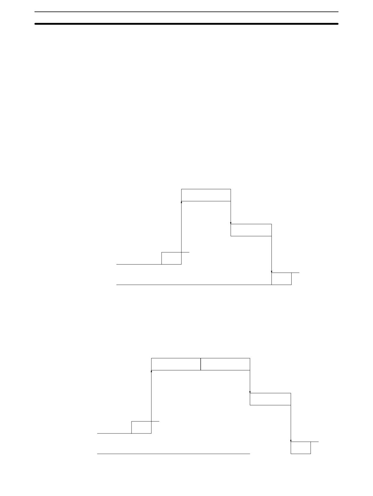
The minimum and maximum I/O response times are shown here, using the fol-
lowing program as an example.
Output
Input
The following conditions are taken as examples for calculating the I/O response
times.
Input ON delay:
8 ms (input time constant: default setting)
Overseeing time:
1 ms (includes I/O refresh for CPM1A)
Instruction execution time:
14 ms
Output ON delay:
10 ms
Peripheral port:
Not used.
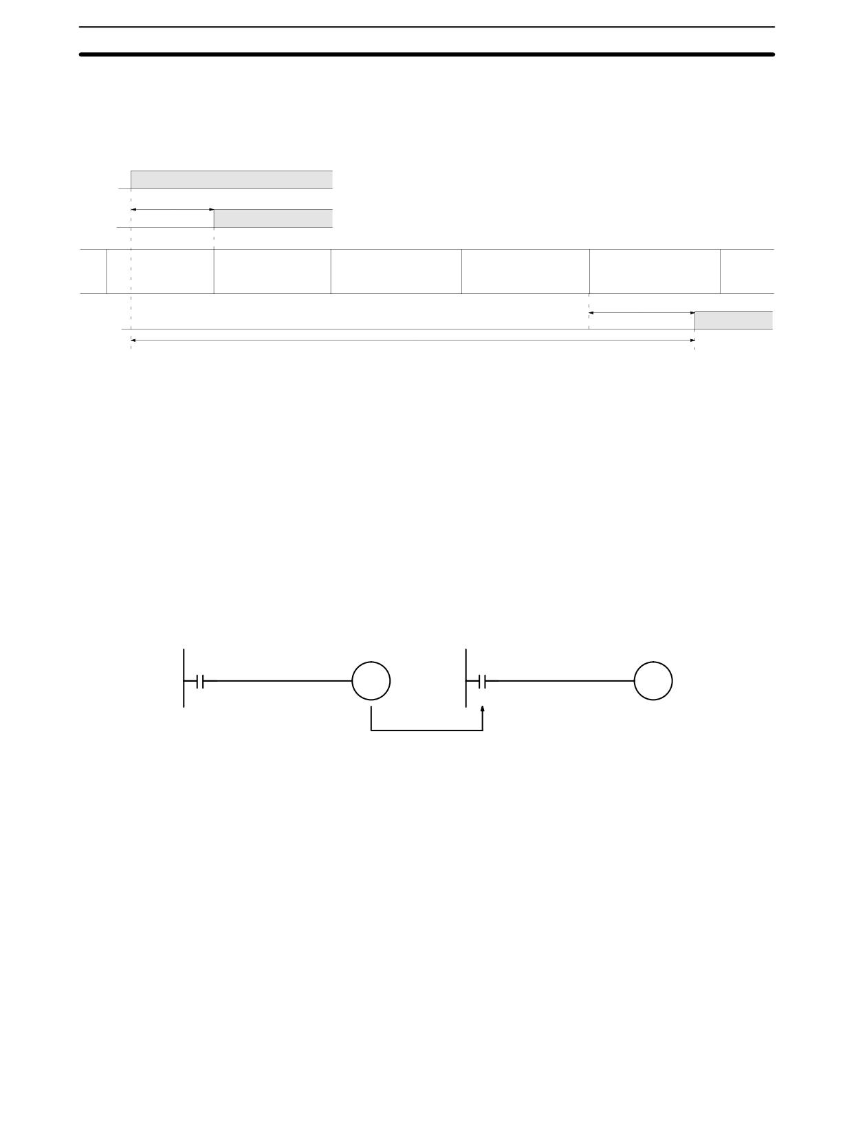
Minimum I/O Response Time The CPM1/CPM1A responds most quickly when it receives an input signal just
prior to I/O refreshing, as shown in the illustration below.
Input
point
Input ON delay (8 ms)
Input
bit
I/O refreshing
Program execution and other processes
I/O refreshing
(15 ms)
Output ON delay (10 ms)
Output
point
Min. I/O response time = 8+15+10 = 33 ms
510
CPM1/CPM1A Cycle Time and I/O Response Time
Section
8-1
Maximum I/O Response Time The CPM1/CPM1A takes longest to respond when it receives the input signal
just after the input refresh phase of the cycle, as shown in the illustration below.
In that case, a delay of approximately one cycle will occur.
Input
point
Input ON delay (8 ms)
Input
bit
Program execution
Program execution
I/O refreshing
I/O refreshing
I/O refreshing
and other processes
and other processes
(15 ms)
(15 ms)
Output ON delay (10 ms)
Output
point
Max. I/O response time = 8+15 × 2+10 = 48 ms
8-1-4
One-to-one PC Link I/O Response Time
When two CPM1/CPM1As are linked 1:1, the I/O response time is the time re-
quired for an input executed at one of the CPM1/CPM1As to be output to the
other CPM1/CPM1A by means of 1:1 PC Link communications.
The minimum and maximum I/O response times are shown here, using as an
example the following instructions executed at the master and the slave. In this
example, communications proceed from the master to the slave.
Master
Slave
Output (LR)
Input
Output
Input
(LR)
The following conditions are taken as examples for calculating the I/O response
times. In CPM1/CPM1A PCs, LR area words LR 00 to LR 15 are used in 1:1 data
links and the transmission time is fixed at 12 ms.
Input ON delay:
8 ms (input time constant: default setting)
Master cycle time:
10 ms
Slave cycle time:
15 ms
Output ON delay:
10 ms
Peripheral port:
Not used.
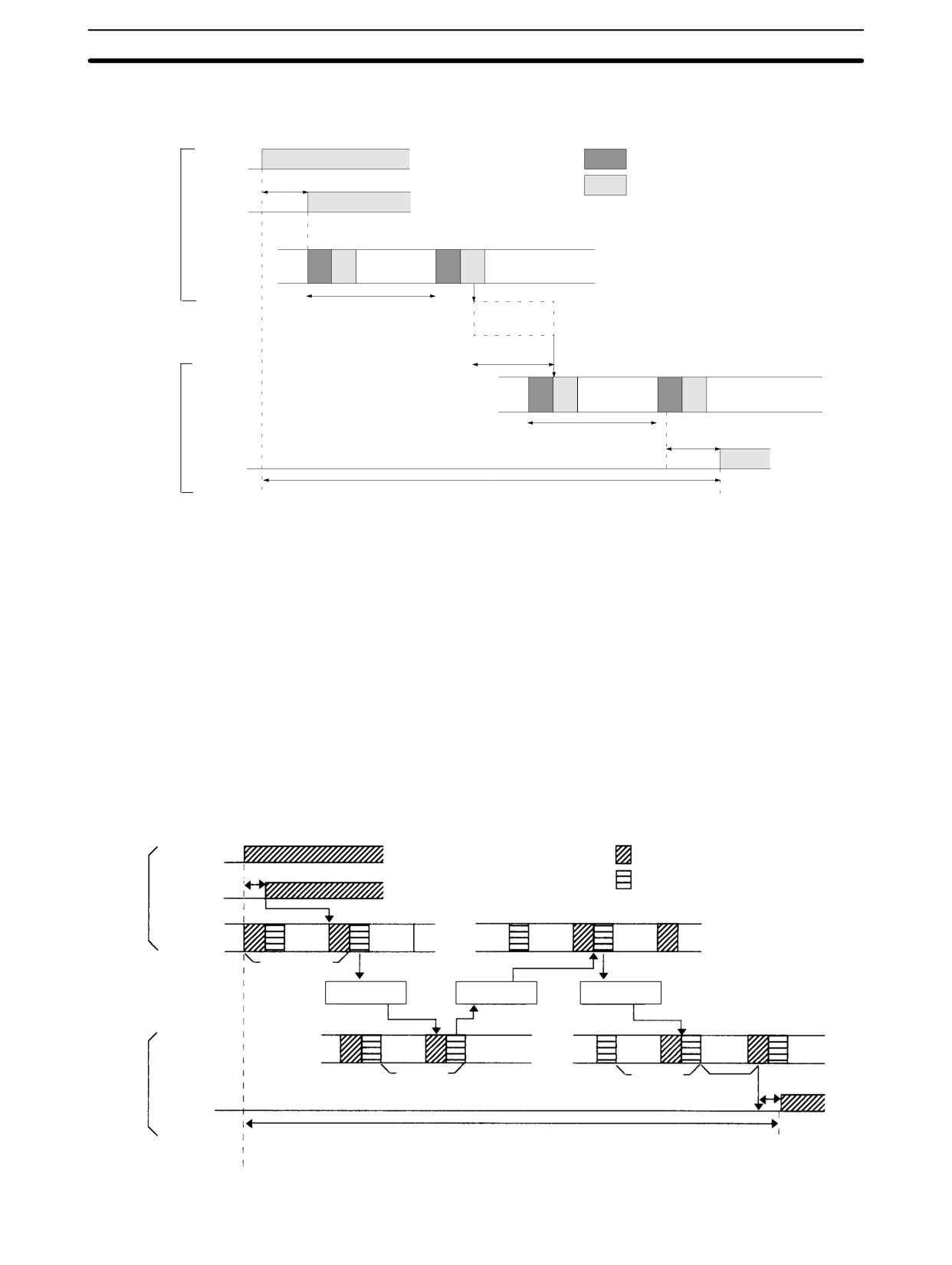
Minimum I/O Response Time The CPM1/CPM1A responds most quickly under the following circumstances:
1, 2, 3...
1. The CPM1/CPM1A receives an input signal just prior to the input refresh
phase of the cycle.
2. The Master’s communications servicing occurs just as the Master-to-Slave
transmission begins.
511
CPM1/CPM1A Cycle Time and I/O Response Time
Section
8-1
3. The Slave’s communications servicing occurs just after the transmission is
completed.
Input
I/O refresh
point
Input ON delay (8 ms)
Overseeing, communica-
tions, etc.
Input
bit
Master
Program
CPU
processing
execution
Master’s cycle time (10 ms)
Master to
Slave
Transmission time (12 ms)
CPU
Program
processing
execution
Output ON
Slave
Slave’s cycle time (15 ms)
delay (10 ms)
Output
point
Min. I/O response time = 8+10+12+15+10 = 55 ms
Calculation formula = Input ON response time + Master’s cycle time + Slave’s
cycle time + Output ON response time
Maximum I/O Response Time The CPM1/CPM1A takes the longest to respond under the following circum-
stances:
1, 2, 3...
1. The CPM1/CPM1A receives an input signal just after the input refresh
phase of the cycle.
2. The Master’s communications servicing just misses the Master-to-Slave
transmission.
3. The transmission is completed just after the Slave’s communications servic-
ing ends.
I/O Maximum Response Time Input ON response time + Master’s cycle time x 2 + Transmission time x 3 + Out-
put ON response time
Input
I/O refresh
point
Input ON response time
Peripheral port servicing
Master
Input
bit
Program
Program
CPU
Program
Program
execution
execution
execution
execution
processing
Master #1
(Data transmission according to input point)
Trans-
Trans-
Master to Slave
mission
Slave to Master
mission
Master to Slave
Transmission time
time
time
CPU
Program
Program
Program
Program
execution
execution
execution
execution
processing
Slave #1
Slave #2
Output OFF
Slave #3
response time
Slave
Output
point
Maximum I/O response time = 8 + 10 x 2 + 12 x 3 + 15 x 3 + 10 = 119 (ms)
512
CPM1/CPM1A Cycle Time and I/O Response Time
Section
8-1
8-1-5
Interrupt Processing Time
This section explains the processing times involved from the time an interrupt is
executed until the interrupt processing routine is called, and from the time an in-
terrupt processing routine is completed until returning to the initial location. This
explanation applies to input interrupts, interval timer interrupts, and high-speed
counter interrupts.
1, 2, 3...
1. Source of interrupt
2. Interrupt ON delay
3. Wait for completion of interrupt-mask processing
4. Change to interrupt processing
5. Interrupt routing (CPM1A only)
6. Return to initial location
The table below shows the times involved from the generation of an interrupt sig-
nal until the interrupt processing routine is called, and from when the interrupt
processing routine is completed until returning to the original position.
Item
Contents
Time
Interrupt ON delay
This is the delay time from the time the interrupt input bit turns ON until the
100 µs
time that the interrupt is executed. This is unrelated to other interrupts.
Wait for completion of
This is the time during which interrupts are waiting until processing has
See below.
interrupt-mask processing
been completed. This situation occurs when a mask processes is
executed. It is explained below in more detail.
Change to interrupt
This is the time it takes to change processing to an interrupt.
30 µs
processing
Return
This is the time it takes, from execution of RET(93), to return to the proces-
30 µs
sing that was interrupted.
Mask Processing
Interrupts are masked during processing of the operations described below. Un-
til the processing is completed, any interrupts will remain masked for the indi-
cated times.
Generation and clearing of non-fatal errors:
When a non-fatal error is generated and the error contents are registered at
the CPM1, or when an error is being cleared, interrupts will be masked for a
maximum of 100 µs until the processing has been completed.
Online editing:
Interrupts will be masked for a maximum of 600 ms (i.e.: editing DM 6144 to
DM 6655) when online editing is executed during operation. In addition, the
system processing may have to wait for a maximum of 170 µs during this
processing.
Example Calculation
This example shows the interrupt response time (i.e., the time from when the
interrupt input turns ON until the start of the interrupt processing routine) when
input interrupts are used under the conditions shown below.
Minimum Response Time
Interrupt ON delay:
100 µs
Interrupt mask standby time:
0 µs
+
Change-to-interrupt processing:
30 µs
Minimum response time:
130 µs
Maximum Response Time
(Except for the Online Editing of DM 6144 to DM6655)
Interrupt ON delay:
100 µs
Interrupt mask standby time:
170 µs
+
Change-to-interrupt processing:
30 µs
Maximum response time:
300 µs
513
CPM1/CPM1A Cycle Time and I/O Response Time
Section
8-1
In addition to the response time shown above, the time required for executing
the interrupt processing routine itself and a return time of 30 µs must also be ac-
counted for when returning to the process that was interrupted.
8-1-6
CPM1/CPM1A Instruction Execution Times
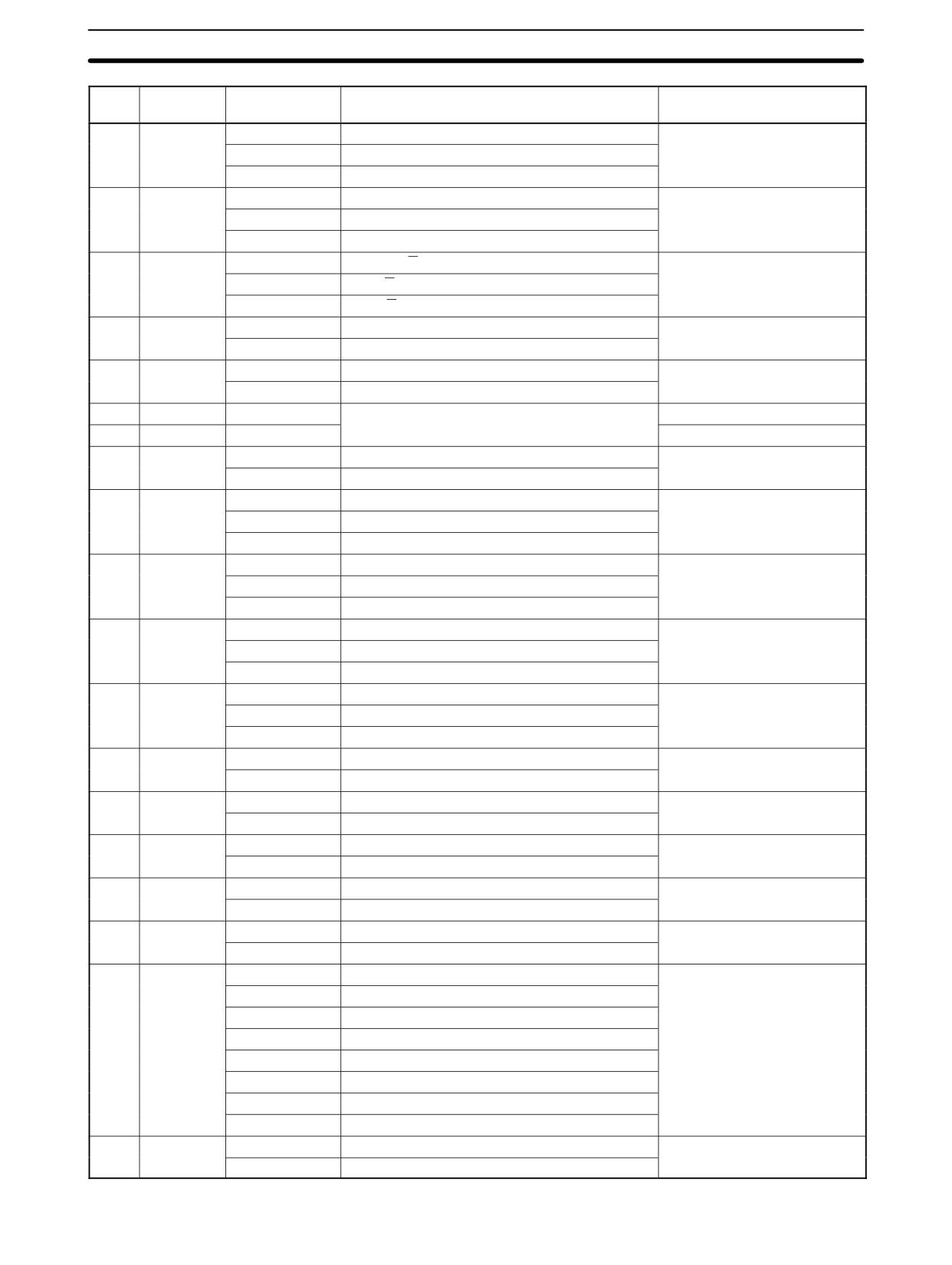
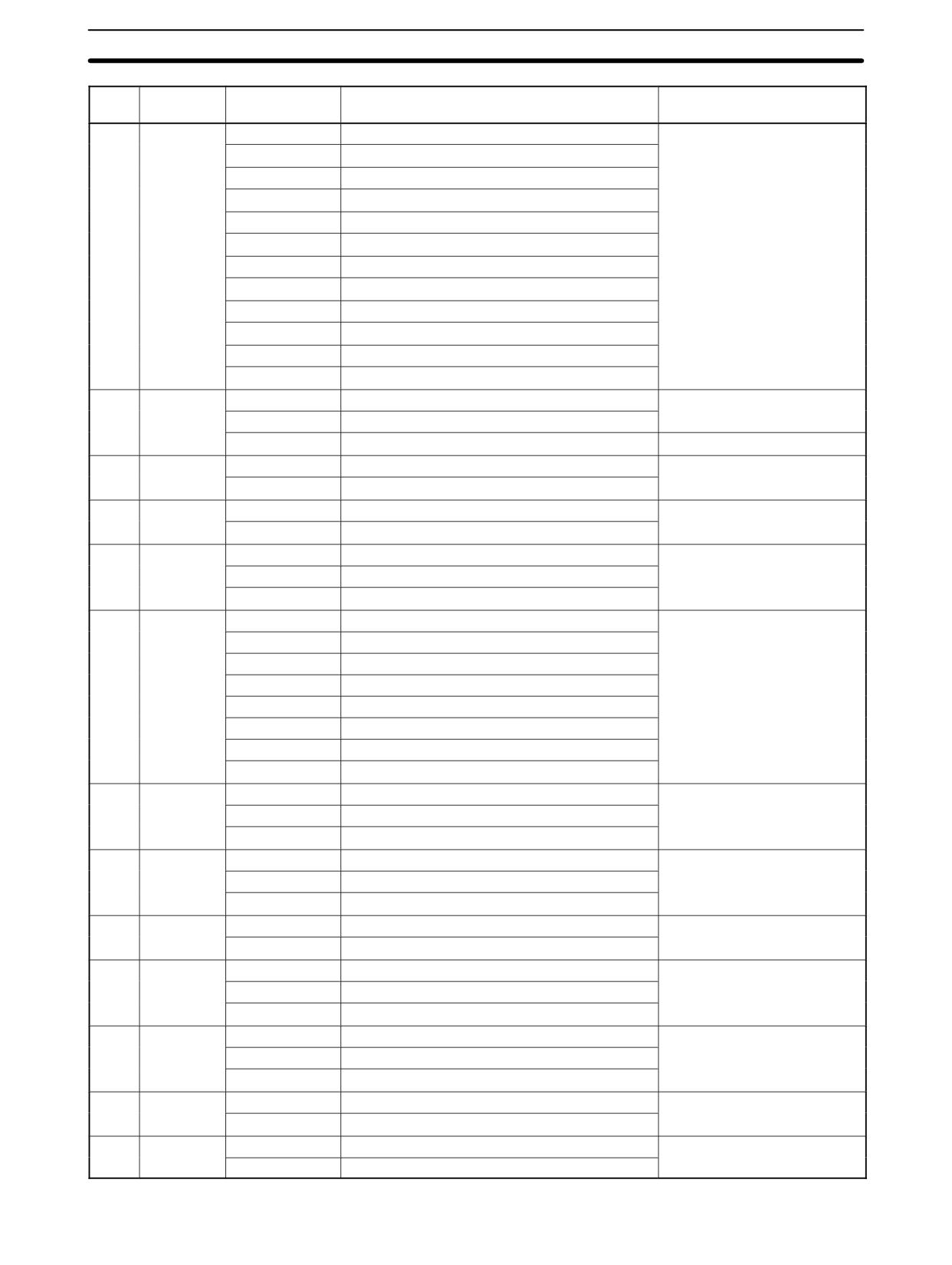
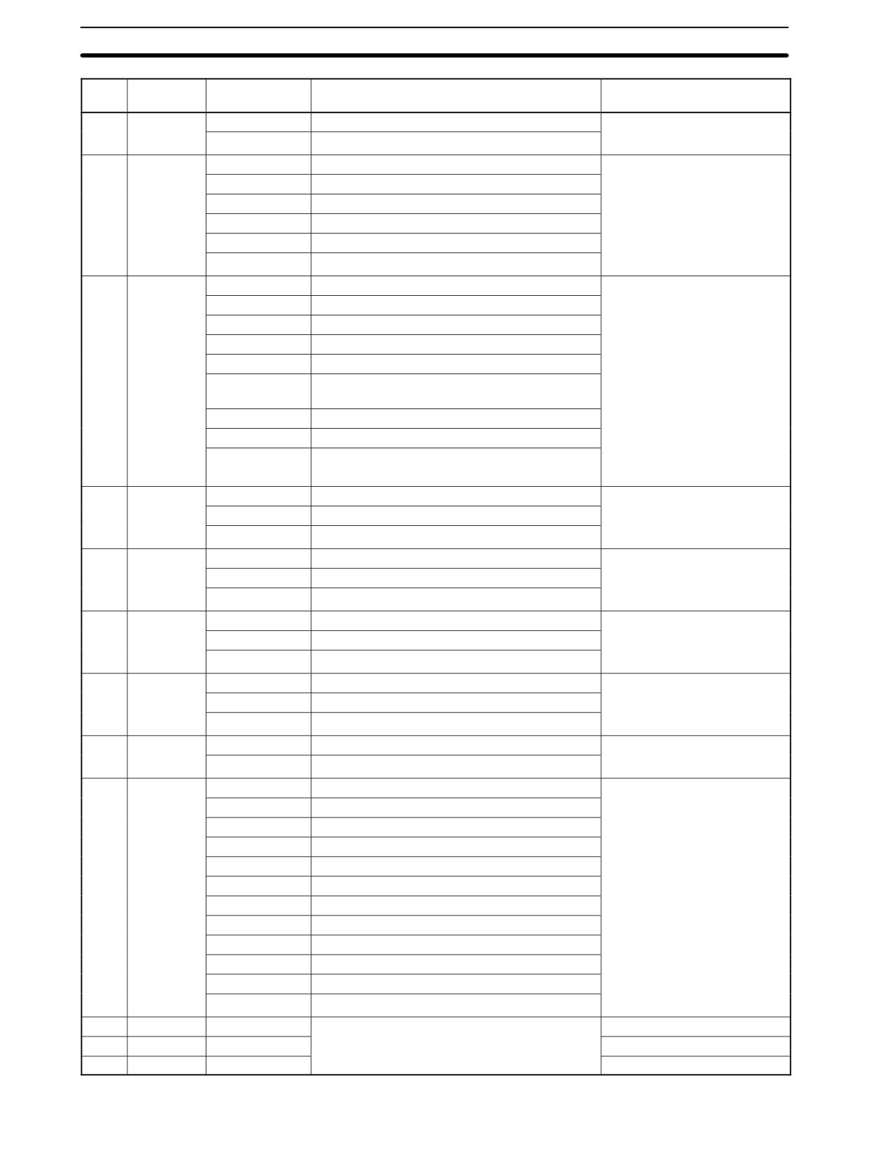
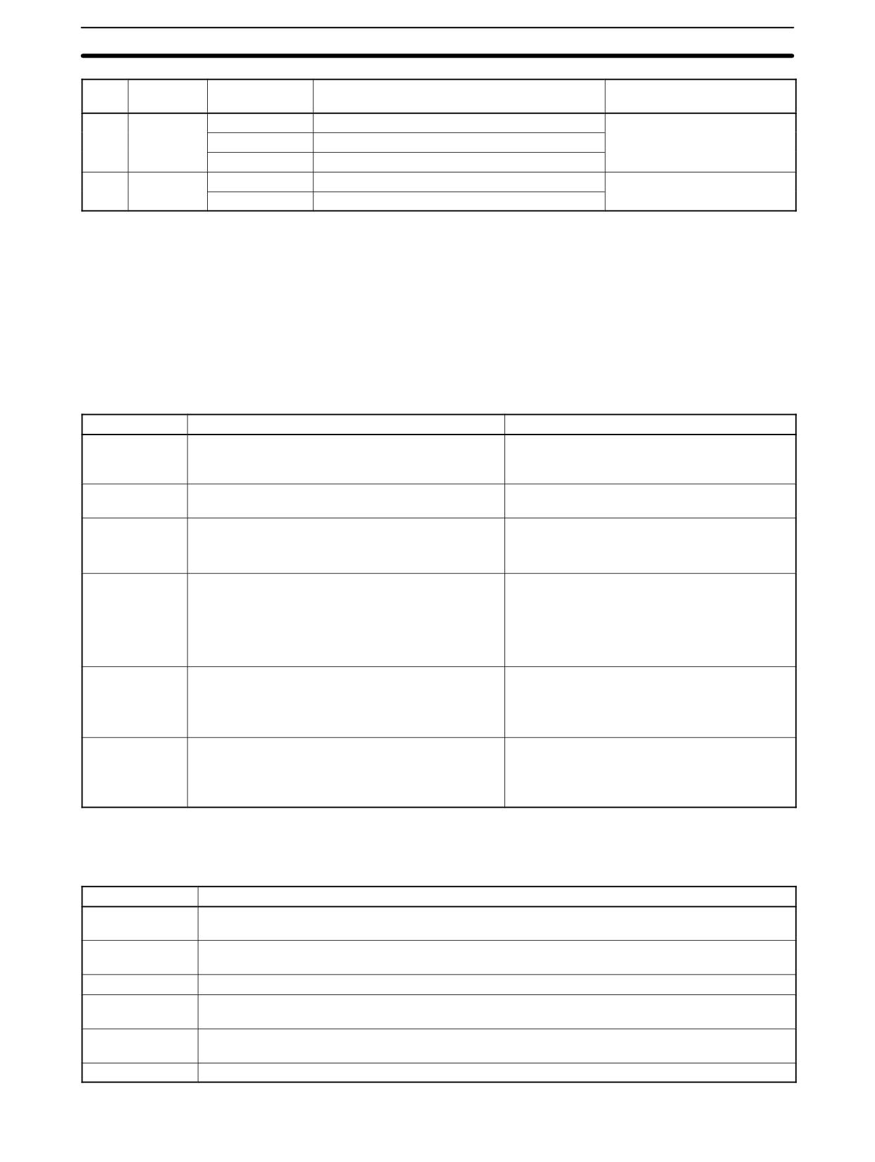
The following table lists the execution times for CPM1/CPM1A instructions.
Basic Instructions
Code
Mnemonic
ON execution
Conditions (Top: min.; bottom: max.)
OFF execution time (µs)
time
(µs
)
RSET
IL
JMP
---
LD
1.72
Any
---
---
LD NOT
---
AND
1.32
---
AND NOT
---
OR
---
OR NOT
---
AND LD
0.72
---
OR LD
---
OUT
4.0
---
OUT NOT
---
SET
5.8
---
RSET
5.9
---
TIM
10.0
Constant for SV
16.2
16.0
6.4
:DM for SV
31.4
31
6.4
---
CNT
12.5
Constant for SV
14.1
6.2
6.6
:DM for SV
29.1
6.2
6.6
Special Instructions
Code
Mnemonic
ON execution
Conditions (Top: min.; bottom: max.)
OFF execution time (µs)
time (µs)
00
NOP
0.36
Any
01
END
10.8
02
IL
4.6
2.6
03
ILC
3.6
3.6
04
JMP
4.3
2.4
05
JME
4.7
4.7
06
FAL
38.5
5.5
07
FALS
5.0
5.4
08
STEP
14.9
11.1
09
SNXT
14.2
7.6
10
SFT
Reset
IL
JMP
21.9
With 1-word shift register
19.7
2.6
2.6
34.1
With 10-word shift register
26.5
2.6
2.6
93.6
With 100-word shift register
60.1
2.6
2.6
11
KEEP
6.2
Any
Reset
IL
JMP
6.1
3.1
3.1
12
CNTR
Reset
IL
JMP
25.8
Constant for SV
16.8
12.2
12.2
41.2
:DM for SV
13
DIFU
11.8
Any
Shift
IL
JMP
10.1
12.2
12.2
14
DIFD
11.0
Any
Shift
IL
JMP
10.0
9.9
2.3
514
CPM1/CPM1A Cycle Time and I/O Response Time
Section
8-1
Code
Mnemonic
ON execution
Conditions (T
op: min.; bottom: max.)
OFF execution time (µs)
time (µs)
15
TIMH
Reset
IL
JMP
19.0
Regular execution, constant for SV
25.7
28.4
15.8
20.2
Interrupt execution, constant for SV
19.0
Regular execution, :DM for SV
41.2
43.6
15.8
20.2
Interrupt execution, :DM for SV
16
WSFT
29.2
With 1-word shift register
5.6
40.7
With 10-word shift register
1.42 ms
With 1,024-word shift register using :DM
17
ASFT
29.6
Shifting a word
5.6
50.2
Shifting 10 words
1.76 ms
Shifting 1,023 words via :DM
20
CMP
15.8
When comparing a constant to a word
5.6
17.2
When comparing two words
46.3
When comparing two :DM
21
MOV
16.3
When transferring a constant to a word
5.6
17.7
When transferring from one word to another
45.5
When transferring :DM to :DM
22
MVN
16.4
When transferring a constant to a word
5.6
17.5
When transferring from one word to another
45.7
When transferring :DM to :DM
23
BIN
31.6
When converting a word to a word
5.6
45.7
When converting :DM to :DM
24
BCD
29.5
When converting a word to a word
5.6
57.3
When converting :DM to :DM
25
ASL
17.3
When shifting a word
5.5
31.3
When shifting :DM
26
ASR
16.9
When shifting a word
5.5
31.1
When shifting :DM
27
ROL
14.5
When rotating a word
5.5
28.5
When rotating :DM
28
ROR
14.5
When rotating a word
5.5
28.5
When rotating :DM
29
COM
18.1
When inverting a word
5.5
32.1
When inverting :DM
30
ADD
29.5
Constant + word → word
5.6
30.9
Word + word → word
72.7
:DM + :DM → :DM
31
SUB
29.3
Constant - word → word
5.6
30.5
Word - word → word
72.5
:DM - :DM → :DM
32
MUL
49.1
Constant word → word
5.6
50.5
Word word → word
95.1
:DM :DM → :DM
33
DIV
47.7
Word ÷ constant → word
5.6
50.9
word ÷ word → word
94.3
:DM ÷ :DM → :DM
34
ANDW
27.1
Constant Ɠ word → word
5.6
28.7
Word Ɠ word → word
70.7
:DM Ɠ :DM → :DM
515
CPM1/CPM1A Cycle Time and I/O Response Time
Section
8-1
Code
Mnemonic
ON execution
Conditions (T
op: min.; bottom: max.)
OFF execution time (µs)
time (µs)
35
ORW
27.1
Constant V word → word
5.6
28.7
Word V word → word
70.7
:DM V :DM → :DM
36
XORW
27.1
Constant V word → word
5.6
28.7
Word V word → word
70.5
:DM V :DM → :DM
37
XNRW
27.0
Constant V word → word
5.6
28.6
Word V word → word
70.5
:DM V :DM → :DM
38
INC
17.9
When incrementing a word
5.5
31.9
When incrementing :DM
39
DEC
18.3
When decrementing a word
5.5
32.3
When decrementing :DM
40
STC
6.3
Any
5.5
41
CLC
6.3
5.5
46
MSG
21.5
With message in words
5.5
35.7
With message in :DM
50
ADB
30.5
Constant + word → word
5.6
32.1
Word + word → word
73.9
:DM + :DM → :DM
51
SBB
30.9
Constant - word → word
5.6
32.7
Word - word → word
74.5
:DM - :DM → :DM
52
MLB
34.7
Constant word → word
5.6
36.3
Word word → word
80.7
:DM :DM → :DM
53
DVB
35.1
Word ÷ constant → word
5.6
36.7
Word ÷ word → word
81.1
:DM ÷ :DM → :DM
54
ADDL
48.9
Word + word → word
5.6
94.7
:DM + :DM → :DM
55
SUBL
48.9
Word - word → word
5.6
94.7
:DM - :DM → :DM
56
MULL
138.7
Word word → word
5.6
184.3
:DM :DM → :DM
57
DIVL
136.7
Word ÷ word → word
5.6
181.3
:DM ÷ :DM → :DM
60
CMPL
30.4
Comparing words
5.6
60.8
Comparing :DM
61
INI
112.0
Starting comparison via word
5.6
126.0
Starting comparison via :DM
48.0
Stopping comparison via word
48.0
Stopping comparison via :DM
120.0
Changing PV via word
128.0
Changing PV via :DM
46.0
Stopping pulse output via word
60.0
Stopping pulse output via :DM
62
PRV
62.2
Designating output via word
5.6
78.0
Designating output via :DM
516
CPM1/CPM1A Cycle Time and I/O Response Time
Section
8-1
Code
Mnemonic
ON execution
Conditions (T
op: min.; bottom: max.)
OFF execution time (µs)
time (µs)
63
CTBL
106.3
Target table with 1 target in words and start
5.6
120.3
Target table with 1 target in :DM and start
775.5
Target table with 16 targets in words and start
799.5
Target table with 16 targets in :DM and start
711.5
Range table in words and start
722.5
Range table in :DM and start
91.9
Target table with 1 target in words
106.3
Target table with 1 target in :DM
693.5
Target table with 16 targets in words
709.5
Target table with 16 targets in :DM
607.5
Range table in words
621.5
Range table in :DM
64
SPED
73.6
Specifying a constant
5.6
75.0
Specifying a word
88.8
Specifying :DM
5.6
65
PULS
62.0
Specifying a word
5.6
78.0
Specifying :DM
67
BCNT
52.6
Counting a word
5.6
4.08 ms
Counting 6,656 words via :DM
68
BCMP
79.6
Comparing constant, results to word
5.6
80.8
Comparing word, results to word
123.2
Comparing :DM, results to :DM
69
STIM
47.5
Word-set one-shot interrupt start
5.6
58.7
:DM-set one-shot interrupt start
47.9
Word-set scheduled interrupt start
59.1
:DM-set scheduled interrupt start
33.5
Word-set timer read
63.5
:DM-set timer read
25.7
Word-set timer stop
54.1
:DM-set timer stop
70
XFER
45.5
When transferring a constant to a word
5.6
47.1
When transferring a word to a word
1.78 ms
When transferring 1,024 words using :DM
71
BSET
28.1
When setting a constant to 1 word
5.6
38.3
When setting word constant to 10 words
1.12 ms
When setting :DM to 1,024 words
73
XCHG
30.5
Word → word
5.6
59.1
:DM → :DM
74
SLD
25.9
Shifting 1 word
5.6
51.7
Shifting 10 word
3.02 ms
Shifting 1024 words using :DM
75
SRD
25.9
Shifting 1 word
5.6
51.7
Shifting 10 word
3.02 ms
Shifting 1,024 words using :DM
76
MLPX
47.7
When decoding word to word
5.6
92.7
When decoding :DM to :DM
77
DMPX
59.5
When encoding word to word
5.6
95.5
When encoding :DM to :DM
517
CPM1/CPM1A Cycle Time and I/O Response Time
Section
8-1
Code
Mnemonic
ON execution
Conditions (T
op: min.; bottom: max.)
OFF execution time (µs)
time (µs)
78
SDEC
51.1
When decoding word to word
5.6
96.3
When decoding :DM to :DM
80
DIST
39.1
When setting a constant to a word + a word
5.6
40.9
When setting a word to a word + a word
84.7
When setting :DM to :DM +:DM
63.4
When setting a constant to a stack
65.0
When setting a word to a stack
109.6
When setting :DM to a stack via :DM
81
COLL
42.6
When setting a constant + a word to a word
5.6
43.6
When setting a word + a word to a word
83.4
When setting :DM + :DM to :DM
78.0
When setting a word + constant to FIFO stack
79.2
When setting a word + word to FIFO stack
1.76 ms
When setting a :DM + :DM to
FIFO stack via :DM
66.8
When setting a word + constant to LIFO stack
68.0
When setting a word + word to LIFO stack
112.0
When setting a :DM + :DM to
LIFO stack via :DM
82
MOVB
32.5
When transferring a constant to a word
5.6
37.5
When transferring from one word to another
79.1
When transferring :DM to :DM
83
MOVD
28.3
When transferring a constant to a word
5.6
33.3
When transferring from one word to another
75.5
When transferring :DM to :DM
84
SFTR
39.3
Shifting 1 word
5.6
52.9
Shifting 10 word
1.42 ms
Shifting 1,024 words using :DM
85
TCMP
57.7
Comparing constant to word-set table
5.6
58.9
Comparing word to word-set table
101.9
Comparing :DM to :DM-set table
86
ASC
56.7
Word → word
5.6
103.9
:DM → :DM
89
INT
32.3
Set masks via word
5.6
46.3
Set masks via :DM
29.1
Clear interrupts via word
43.1
Clear interrupts via :DM
27.3
Read mask status via word
41.5
Read mask status via :DM
29.7
Change counter SV via word
43.7
Change counter SV via :DM
15.3
Mask all interrupts via word
15.3
Mask all interrupts via :DM
15.9
Clear all interrupts via word
15.9
Clear all interrupts via :DM
91
SBS
36.6
Any
5.5
92
SBN
1.7
1.7
93
RET
15.0
2.5
518
CPM2A/CPM2C Cycle Time and I/O Response Time
Section
8-2
Code
Mnemonic
ON execution
Conditions (T
op: min.; bottom: max.)
OFF execution time (µs)
time (µs)
97
IORF
40.0
Refreshing IR 000
6.0
142.6
Refreshing one input word
135.4
Refreshing one output word
99
MCRO
74.0
With word-set I/O operands
5.6
116.4
With :DM-set I/O operands
8-2
CPM2A/CPM2C Cycle Time and I/O Response Time
8-2-1
CPM2A/CPM2C Cycle Time
The processes involved in a single CPM2A/CPM2C cycle are shown in the fol-
lowing table, and their respective processing times are explained. Refer to the
CPM2C-S Operation Manual (W377) for information on the cyclic operation of
the CPM2C-S.
Process
Content
Time requirements
Overseeing
Setting cycle watchdog timer, I/O bus check, UM
0.3 ms
check, clock refreshing, refreshing bits allocated to
new functions.
Program
User program is executed.
Total time for executing instructions. (Varies
execution
according to content of user’s program.)
Cycle time
Automatic delay until minimum cycle time when a
Negligible except for the delay itself when re-
calculation
minimum cycle time is set in DM 6619 of PC Setup.
quired.
Calculation of cycle time.
I/O refreshing
Output information (results of executing program) is
CPM2C CPU Unit:
0.06 ms
written to output bits.
20-point CPM2A CPU Unit:
0.06 ms
30-point CPM2A CPU Unit:
0.3 ms
Input information is read to input bits.
40-point CPM2A CPU Unit:
0.3 ms
60-point CPM2A CPU Unit:
0.54 ms
Expansion I/O Unit:
0.3 ms
RS-232C port
Communications processing when a Programming
0.55 ms min., 5% or less of cycle time up to
servicing
Device or Communications Adapter is connected to
131 ms
the RS-232C port.
(The percentage of cycle time allocated to
RS-232C servicing can be set in DM 6616.)
Peripheral port
Devices connected to peripheral port serviced.
0.55 ms min., 5% or less of cycle time up to
servicing
131 ms
(The percentage of cycle time allocated to pe-
ripheral port servicing can be set in DM 6617.)
Cycle Time and Operations
The effects of the cycle time on CPM2A/CPM2C operations are as shown below.
When a long cycle time is affecting operation, either reduce the cycle time or im-
prove responsiveness with interrupt programs.
Cycle time
Operation conditions
1 ms or longer
TMHH(--) may be inaccurate when TC 000 through TC 003 or TC 008 through TC 255 are used
(operation will be normal for TC 004 through TC 007).
10 ms or longer
TIMH(15) may be inaccurate when TC 004 through TC 255 are used (operation will be normal for
TC 000 through TC 003).
20 ms or longer
Programming using the 0.02-second Clock Bit (SR 25401) may be inaccurate.
100 ms or longer
TIM may be inaccurate. Programming using the 0.1-second Clock Bit (SR 25500) may be inaccu-
rate. A CYCLE TIME OVER error is generated (SR 25309 will turn ON).
120 ms or longer
The FALS 9F monitoring time SV is exceeded. A system error (FALS 9F) is generated, and opera-
tion stops.
200 ms or longer
Programming using the 0.2-second Clock Bit (SR 25501) may be inaccurate.
519
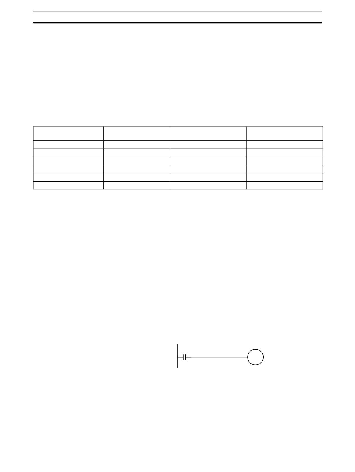
CPM2A/CPM2C Cycle Time and I/O Response Time
Section
8-2
Cycle Time Example
In this example, the cycle time is calculated for a CPM2A/CPM2C CPU Unit with
30 I/O points (18 input points and 12 output points). The I/O is configured as fol-
lows:
18 inputs:
2 words (00000 to 00011, 00100 to 00105)
12 outputs:
2 words (01000 to 01007, 01100 to 01103)
The rest of the operating conditions are assumed to be as follows:
User’s program:500 instructions (consists of only LD and OUT)
Cycle time:
Variable (no minimum set)
The average processing time for a single instruction in the user’s program is as-
sumed to be 1.26 µs. The cycle times are as shown in the following table.
Process
Calculation method
Time with
Time without
Programming Device
Programming Device
1. Overseeing
Fixed
0.3 ms
0.3 ms
2. Program execution
1.26 × 500 (µs)
0.6 ms
0.6 ms
3. Cycle time calculation
Negligible
0 ms
0 ms
4. I/O refreshing
Fixed
0.3 ms (CPM2C: 0.06 ms)
0.3 ms (CPM2C: 0.06 ms)
5. Peripheral port servicing
Minimum time
0.55 ms
0 ms
Cycle time
(1) + (2) + (3) + (4) + (5)
1.75 ms (CPM2C: 1.51 ms)
1.2 ms (CPM2C: 0.96 ms)
Note
1. The cycle time can be read from the PC via a Programming Device.
2. The maximum and current cycle time are stored in AR 14 and AR 15.
3. The cycle time can vary with actual operating conditions and will not neces-
sarily agree precisely with the calculated value.
8-2-2
I/O Response Time
The I/O response time is the time it takes after an input signal has been received
(i.e., after an input bit has turned ON) for the PC to check and process the in-
formation and to output a control signal (i.e., to output the result of the proces-
sing to an output bit). The I/O response time varies according to the timing and
processing conditions.
The minimum and maximum I/O response times are shown here, using the fol-
lowing program as an example.
Output
Input
The following conditions are taken as examples for calculating the I/O response
times.
Input ON delay:
10 ms (input time constant: default setting)
Overseeing time:
1 ms (includes I/O refreshing)
Instruction execution time:
14 ms
Output ON delay:
15 ms
Communications ports:
Not used.
520
CPM2A/CPM2C Cycle Time and I/O Response Time
Section
8-2
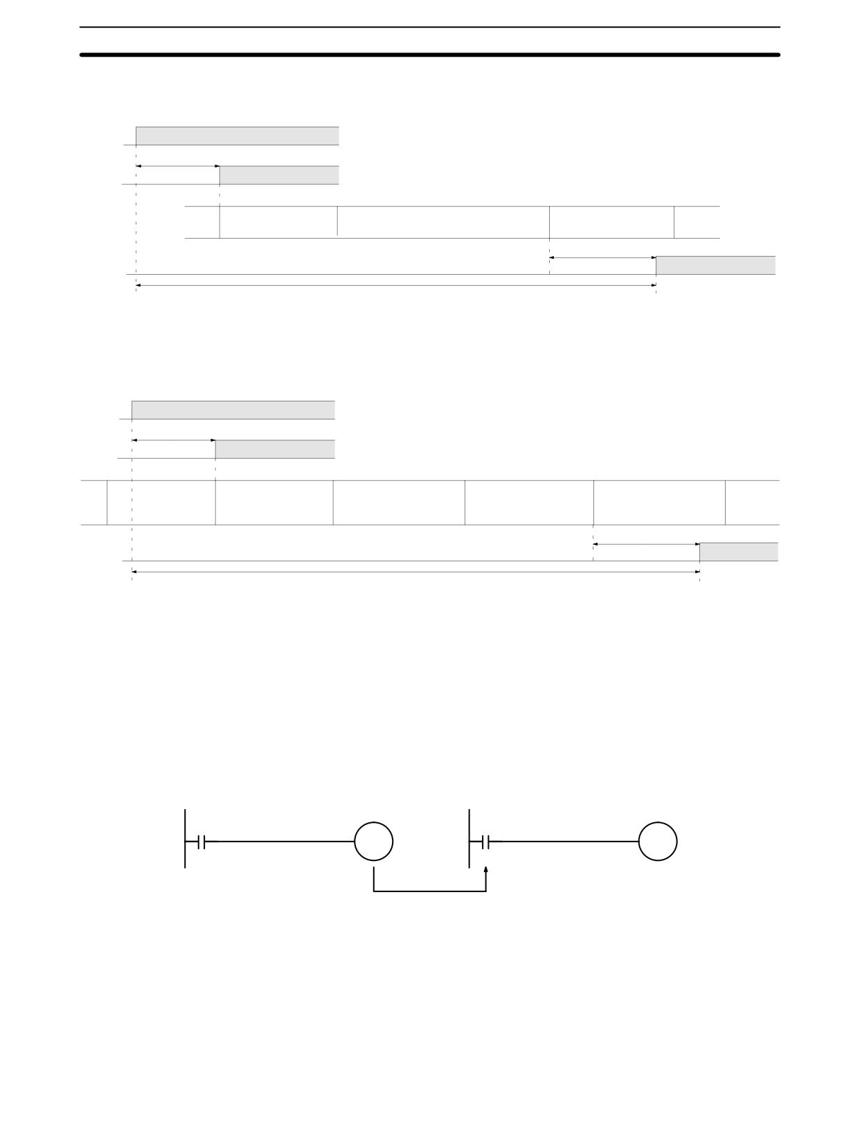
Minimum I/O Response Time The CPM2A/CPM2C responds most quickly when it receives an input signal just
prior to I/O refreshing, as shown in the illustration below.
Input
point
Input ON delay (10 ms)
Input
bit
I/O refreshing
Program execution and other processes
I/O refreshing
(15 ms)
Output ON delay (10 ms)
Output
point
Min. I/O response time = 10+15+15 = 40 ms
Maximum I/O Response Time The CPM2A/CPM2C takes longest to respond when it receives the input signal
just after the input refresh phase of the cycle, as shown in the illustration below.
In that case, a delay of approximately one cycle will occur.
Input
point
Input ON delay (10 ms)
Input
bit
Program execution
Program execution
I/O refreshing
I/O refreshing
I/O refreshing
and other processes
and other processes
(15 ms)
(15 ms)
Output ON delay (10 ms)
Output
point
Max. I/O response time = 10+15 × 2+15 = 55 ms
8-2-3
One-to-one PC Link I/O Response Time
When two CPM2A/CPM2Cs are linked 1:1, the I/O response time is the time re-
quired for an input executed at one of the CPM2A/CPM2Cs to be output to the
other CPM2A/CPM2C by means of 1:1 PC Link communications.
The minimum and maximum I/O response times are shown here, using as an
example the following instructions executed at the master and the slave. In this
example, communications proceed from the master to the slave.
Master
Slave
Output (LR)
Input
Output
Input
(LR)
The following conditions are taken as examples for calculating the I/O response
times. In CPM2A/CPM2C PCs, LR area words LR 00 to LR 15 are used in 1:1
data links and the transmission time is fixed at 21 ms.
Input ON delay:
10 ms (input time constant: default setting)
Master cycle time:
10 ms
Slave cycle time:
15 ms
Output ON delay:
15 ms
Minimum I/O Response Time The CPM2A/CPM2C responds most quickly under the following circumstances:
521
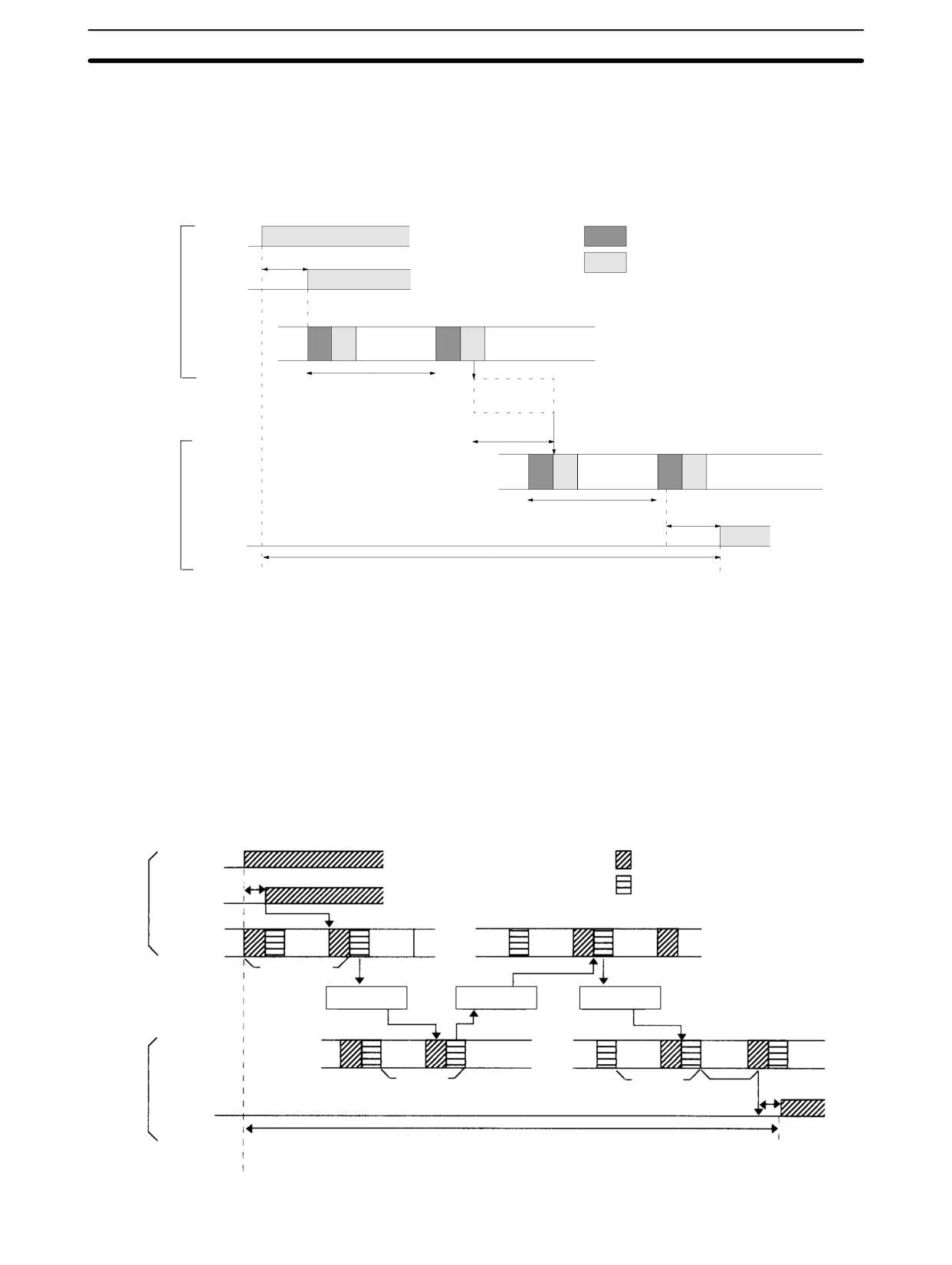
CPM2A/CPM2C Cycle Time and I/O Response Time
Section
8-2
1, 2, 3...
1. The CPM2A/CPM2C receives an input signal just prior to the input refresh
phase of the cycle.
2. The Master’s communications servicing occurs just as the Master-to-Slave
transmission begins.
3. The Slave’s communications servicing occurs just after the transmission is
completed.
Input
I/O refresh
point
Input ON delay (10 ms)
Overseeing, communications
Input
servicing, etc.
bit
Master
Program
CPU
execution
processing
Master’s cycle time (10 ms)
Master to
Slave
Transmission time (21 ms)
CPU
Program
processing
execution
Output ON
Slave
Slave’s cycle time (15 ms)
delay (10 ms)
Output
point
Min. I/O response time = 10+10+12+15+15 = 62 ms
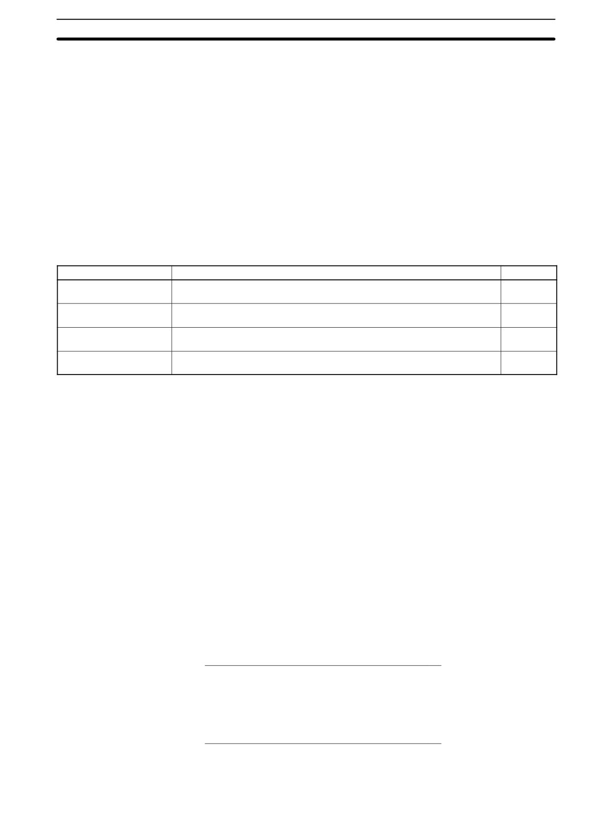
Maximum I/O Response Time The CPM2A/CPM2C takes the longest to respond under the following circum-
stances:
1, 2, 3...
1. The CPM2A/CPM2C receives an input signal just after the input refresh
phase of the cycle.
2. The Master’s communications servicing just misses the Master-to-Slave
transmission.
3. The transmission is completed just after the Slave’s communications servic-
ing ends.
I/O Maximum Response Time Input ON response time + Master’s cycle time × 2 + Transmission time × 3 +
Slave’s cycle time × 2 + Output ON response time
Input
I/O refresh
point
Input ON response time
Peripheral port servicing
Master
Input
bit
CPU
Program
Program
Program
Program
execution
execution
execution
execution
processing
Master #1
(Data transmission according to input point)
Trans-
Trans-
Master to Slave
mission
Slave to Master
mission
Master to Slave
Transmission time
time
time
CPU
Program
Program
Program
Program
execution
execution
execution
execution
processing
Slave #1
Slave #2
Output OFF
Slave #3
response time
Slave
Output
point
Maximum I/O response time = 10 + 10 × 2 + 12 × 3 + 15 × 2 + 15 = 111 (ms)
522
CPM2A/CPM2C Cycle Time and I/O Response Time
Section
8-2
8-2-4
Interrupt Processing Time
This section explains the processing times involved from the time an interrupt is
executed until the interrupt processing routine is called, and from the time an in-
terrupt processing routine is completed until returning to the initial location. This
explanation applies to input interrupts, interval timer interrupts, and high-speed
counter interrupts.
1, 2, 3...
1. Source of interrupt
2. Interrupt ON delay
3. Wait for completion of interrupt-mask processing
4. Change to interrupt processing
5. Interrupt routing (CPM1A/CPM2A/CPM2C only)
6. Return to initial location
The table below shows the times involved from the generation of an interrupt sig-
nal until the interrupt processing routine is called, and from when the interrupt
processing routine is completed until returning to the original position.
Item
Contents
Time
Interrupt ON delay
This is the delay time from the time the interrupt input bit turns ON until the
100 µs
time that the interrupt is executed. This delay does not affect other interrupts.
Wait for completion of
When a process that disables (masks) the interrupt is being executed, this is
See below.
interrupt-mask processing
the time required for that process to be completed.
Change to interrupt
This is the time it takes to change processing to the interrupt process.
30 µs
processing
Return
This is the time it takes, from execution of RET(93), to return to the processing
30 µs
that was interrupted.
Mask Processing
Interrupts are masked during processing of the operations described below. Un-
til the processing is completed, any interrupts will remain masked for the indi-
cated times.
Generation and clearing of non-fatal errors:
Interrupts will be masked for up to 100 µs when a non-fatal error has been
generated and the error contents are being registered in the PC, or when an
error is being cleared.
Online editing:
Operation will stop and interrupts will be masked for up to 600 ms (for
DM 6144 to DM 6655) when online editing is executed or the settings are
changed with STUP(--) during operation. The program or PC Setup can be
overwritten during that delay.
In addition to the online editing delay, interrupts may be masked for up to
170 µs for system processing.
Example Calculation
This example shows the interrupt response time (i.e., the time from when the
interrupt input turns ON until the start of the interrupt processing routine) when
input interrupts are used under the conditions shown below.
Minimum Response Time
Interrupt ON delay:
100 µs
Interrupt mask standby time:
0 µs
+
Change-to-interrupt processing:
30 µs
Minimum response time:
130 µs
Maximum Response Time
(Except for the Online Editing of DM 6144 to DM 6655)
Interrupt ON delay:
100 µs
Interrupt mask standby time:
170 µs
+
Change-to-interrupt processing:
30 µs
Maximum response time:
300 µs
523
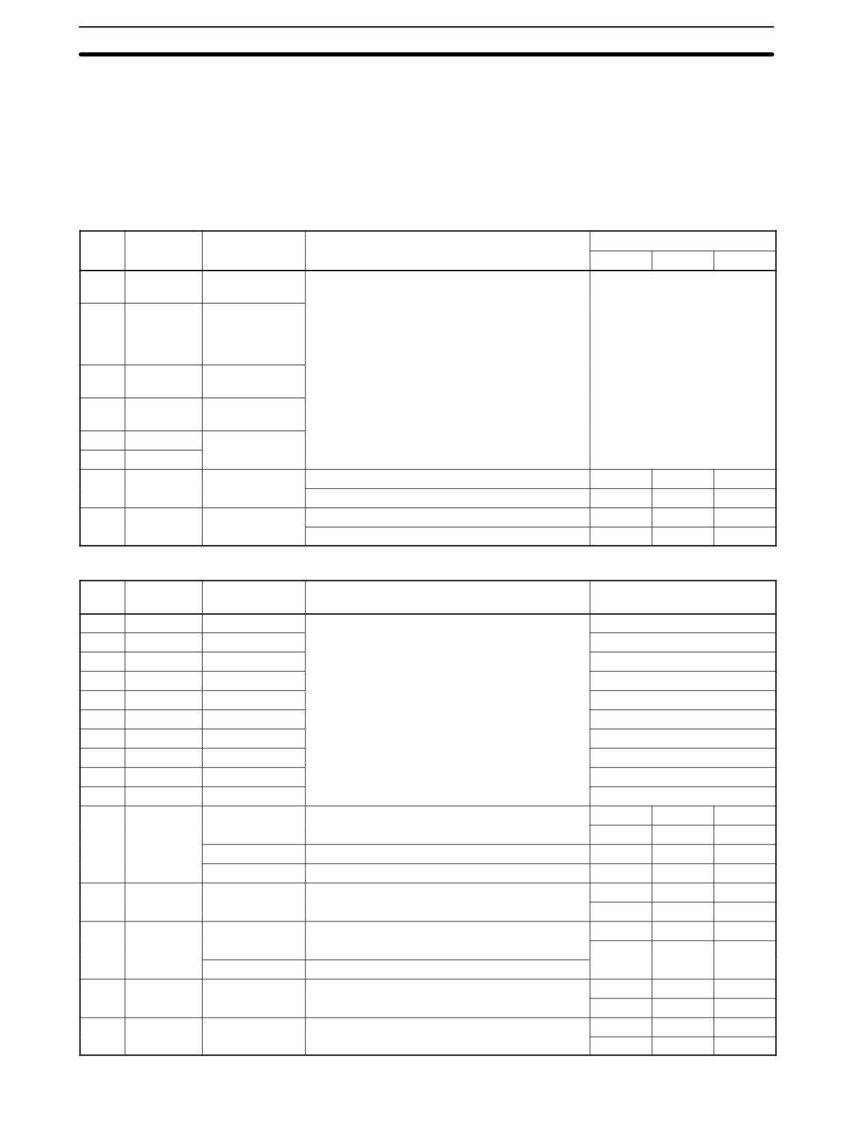
CPM2A/CPM2C Cycle Time and I/O Response Time
Section
8-2
In addition to the response time shown above, the time required for executing
the interrupt processing routine itself and a return time of 30 µs must also be ac-
counted for when returning to the process that was interrupted.
8-2-5
CPM2A/CPM2C Instruction Execution Times
The following table lists the execution times for CPM2A/CPM2C (including the
CPM2C-S) instructions.
Basic Instructions
Code
Mnemonic
ON execution
Conditions (Top: min.; bottom: max.)
OFF execution time (µs)
ti
me
(µs
)
RSET
IL
JMP
---
LD
0.64
Any
---
---
LD NOT
---
AND
0.52
---
AND NOT
---
OR
---
OR NOT
---
AND LD
0.26
---
OR LD
---
OUT
1.88
---
OUT NOT
---
SET
2.58
---
RSET
---
TIM
4.76
Constant for SV
7.8
7.6
2.9
:DM for SV
15.6
15.4
2.9
---
CNT
4.50
Constant for SV
6.8
2.9
3.1
:DM for SV
14.5
2.9
3.1
Special Instructions
Code
Mnemonic
ON execution
Conditions (Top: min.; bottom: max.)
OFF execution time (µs)
time (µs)
00
NOP
0.15
Any
01
END
6.2
02
IL
1.1
2.1
03
ILC
1.6
1.6
04
JMP
0.95
1.8
05
JME
2.1
2.1
06
FAL
20.5
2.5
07
FALS
2.9
2.5
08
STEP
7.3
6.0
09
SNXT
5.1
3.6
10
SFT
Reset
IL
JMP
10.4
With 1-word shift register
9.2
0.98
0.98
15.3
With 10-word shift register
11.9
1.0
1.0
39.6
With 53-word shift register
26.2
1.0
1.0
11
KEEP
3.2
Any
Reset
IL
JMP
3.1
1.2
1.3
12
CNTR
Reset
IL
JMP
10.9
Constant for SV
7.9
5.5
5.6
18.8
:DM for SV
13
DIFU
5.5
Any
Shift
IL
JMP
5.1
4.8
0.96
14
DIFD
5.3
Any
Shift
IL
JMP
5.4
4.7
0.97
524
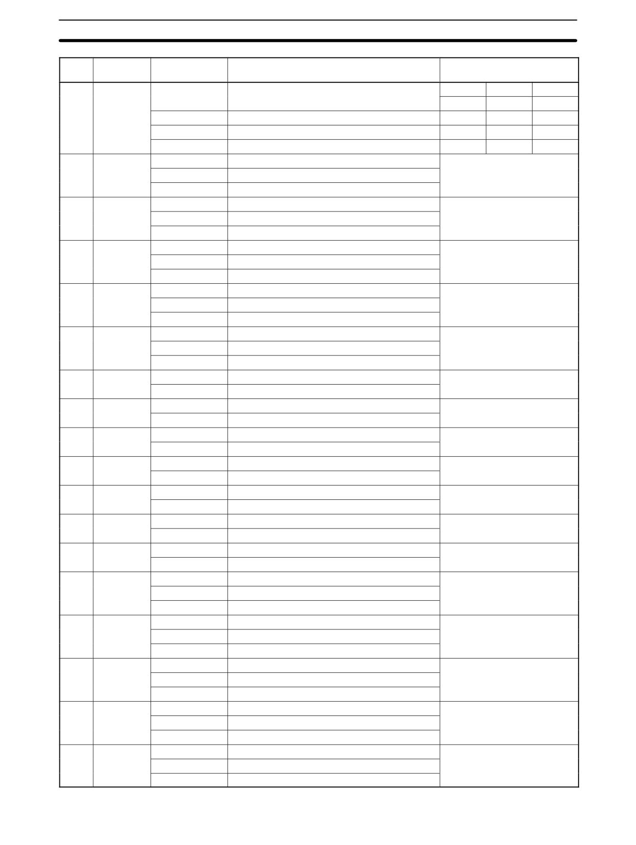
CPM2A/CPM2C Cycle Time and I/O Response Time
Section
8-2
Code
Mnemonic
ON execution
Conditions (T
op: min.; bottom: max.)
OFF execution time (µs)
time (µs)
15
TIMH
Reset
IL
JMP
9.0
Regular execution, constant for SV
13.0
12.6
6.1
9.6
Interrupt execution, constant for SV
14.4
14.0
7.5
9.8
Regular execution, :DM for SV
20.8
20.5
6.1
10.7
Interrupt execution, :DM for SV
22.2
22.0
7.5
16
WSFT
14.0
With 1-word shift register
2.6
18.6
With 10-word shift register
1.15 ms
With 2,048-word shift register using :DM
17
ASFT
13.0
Shifting 1 word
2.6
22.9
Shifting 10 words
1.51 ms
Shifting 2,048 words via :DM
20
CMP
7.0
When comparing a constant to a constant
2.6
8.3
When comparing two words
12.1
When comparing two :DM
21
MOV
7.8
When transferring a constant to a word
2.6
8.4
When transferring from one word to another
22.8
When transferring :DM to :DM
22
MVN
7.9
When transferring a constant to a word
2.6
8.4
When transferring from one word to another
22.8
When transferring :DM to :DM
23
BIN
15.8
When converting a word to a word
2.6
30.3
When converting :DM to :DM
24
BCD
14.6
When converting a word to a word
2.6
29.0
When converting :DM to :DM
25
ASL
8.6
When shifting a word
2.5
15.8
When shifting :DM
26
ASR
8.4
When shifting a word
2.5
15.6
When shifting :DM
27
ROL
7.3
When rotating a word
2.5
14.5
When rotating :DM
28
ROR
7.3
When rotating a word
2.5
14.5
When rotating :DM
29
COM
8.9
When inverting a word
2.5
16.1
When inverting :DM
30
ADD
14.7
Constant + constant → word
2.6
16.0
Word + word → word
37.6
:DM + :DM → :DM
31
SUB
14.6
Constant - constant → word
2.6
15.8
Word - word → word
37.5
:DM - :DM → :DM
32
MUL
26.8
Constant constant → word
2.6
28.3
Word word → word
51.0
:DM :DM → :DM
33
DIV
25.9
Constant ÷ constant → word
2.6
27.5
word ÷ word → word
50.1
:DM ÷ :DM → :DM
34
ANDW
12.3
Constant Ɠ constant → word
2.6
13.8
Word Ɠ word → word
35.4
:DM Ɠ :DM → :DM
525
CPM2A/CPM2C Cycle Time and I/O Response Time
Section
8-2
Code
Mnemonic
ON execution
Conditions (T
op: min.; bottom: max.)
OFF execution time (µs)
time (µs)
35
ORW
12.3
Constant V constant → word
2.6
13.8
Word V word → word
35.4
:DM V :DM → :DM
36
XORW
12.3
Constant V constant → word
2.6
13.8
Word V word → word
35.4
:DM V :DM → :DM
37
XNRW
12.3
Constant V constant → word
2.6
13.8
Word V word → word
35.5
:DM V :DM → :DM
38
INC
8.8
When incrementing a word
2.5
15.9
When incrementing :DM
39
DEC
8.9
When decrementing a word
2.5
16.1
When decrementing :DM
40
STC
3.0
Any
2.5
41
CLC
3.0
2.5
46
MSG
9.9
With message in words
2.5
17.8
With message in :DM
47
RXD
71.9
Word specification, 1 byte input
2.6
314.5
:DM specification, 256 bytes input
48
TXD
32.4
Word specification, 1 byte input, RS-232C
2.6
264.5
:DM specification, 256 bytes input, RS-232C
27.7
Word specification, 1 byte input, Host Link
42.2
:DM specification, 256 bytes input, Host Link
50
ADB
14.1
Constant + constant → word
2.6
15.6
Word + word → word
37.4
:DM + :DM → :DM
51
SBB
14.4
Constant - constant → word
2.6
15.9
Word - word → word
37.7
:DM - :DM → :DM
52
MLB
16.8
Constant constant → word
2.6
18.5
Word word → word
41.2
:DM :DM → :DM
53
DVB
16.9
Constant ÷ constant → word
2.6
18.6
Word ÷ word → word
41.3
:DM ÷ :DM → :DM
54
ADDL
25.3
Word + word → word
2.6
48.6
:DM + :DM → :DM
55
SUBL
25.3
Word - word → word
2.6
48.6
:DM - :DM → :DM
56
MULL
79.1
Word word → word
2.6
102.1
:DM :DM → :DM
57
DIVL
73.9
Word ÷ word → word
2.6
98.6
:DM ÷ :DM → :DM
58
BINL
23.9
When converting word data to a word
2.6
38.5
When converting :DM to :DM
59
BCDL
19.1
When converting word data to a word
2.6
33.7
When converting :DM to :DM
60
CMPL
14.8
Comparing words
2.6
30.6
Comparing :DM
526
CPM2A/CPM2C Cycle Time and I/O Response Time
Section
8-2
Code
Mnemonic
ON execution
Conditions (T
op: min.; bottom: max.)
OFF execution time (µs)
time (µs)
61
INI
68.8
Starting high-speed counter comparison
2.6
12.0
Stopping high-speed counter comparison
43.3
Specifying a constant when changing high-
speed counter PV
51.8
Specifying :DM when changing high-speed
counter PV
42.8
Specifying increment mode via constant
50.8
Specifying increment mode via :DM
60.1
Stopping pulse output
42.7
Specifying a constant when changing pulse out-
put PV
50.7
Specifying :DM when changing pulse output
PV
17.8
Stopping synchronized control of high-speed
counter
20.0
Specifying a constant when changing interrupt
counter PV
27.6
Specifying :DM when changing interrupt
counter PV
62
PRV
36.9
Reading high-speed counter PV via word
2.6
44.7
Reading high-speed counter PV :DM
36.6
Specifying increment mode via word
44.3
Specifying increment mode via :D
38.5
Specifying a word when using synchronized
control
46.2
Specifying :DM when using synchronized con-
trol
20.2
Reading high-speed counter pulse output status
via word
27.4
Reading high-speed counter pulse output status
via :DM
24.4
Reading high-speed counter read range com-
parison results via word
32.4
Reading high-speed counter read range com-
parison results via :DM
39.9
Reading pulse output PV via word
47.8
Reading pulse output PV via :DM
20.1
Reading interrupt counter PV via word
27.1
Reading interrupt counter PV via :DM
527
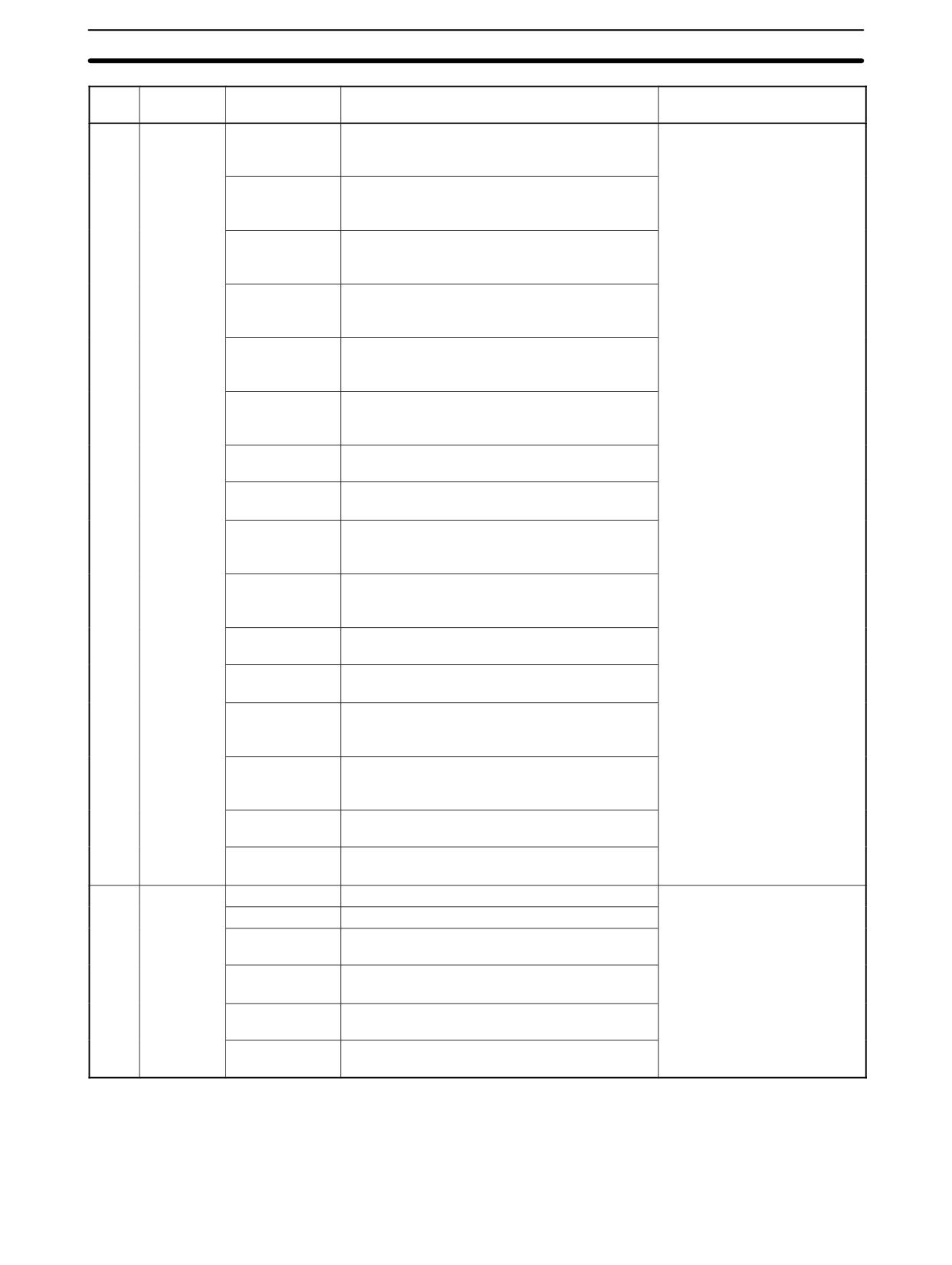
CPM2A/CPM2C Cycle Time and I/O Response Time
Section
8-2
Code
Mnemonic
ON execution
Conditions (T
op: min.; bottom: max.)
OFF execution time (µs)
time (µs)
63
CTBL
186.0
Registering a target value comparison table and
2.6
starting comparison in incrementing/decrement-
ing pulse input mode via word
807.5
Registering a target value comparison table and
starting comparison in incrementing/decrement-
ing pulse input mode via :DM
185.8
Registering a target value comparison table and
starting comparison in incrementing mode via
word
781.9
Registering a target value comparison table and
starting comparison in incrementing mode via
:DM
410.0
Registering a range comparison table and start-
ing comparison in incrementing/decrementing
pule input mode via word
418.9
Registering a range comparison table and start-
ing comparison in incrementing/decrementing
pule input mode via :DM
380.6
Registering a range comparison table and start-
ing comparison in incrementing mode via word
399.7
Registering a range comparison table and start-
ing comparison in incrementing mode via :DM
183.4
Only registering a target value comparison table
in incrementing/decrementing pulse input mode
via word
810.3
Only registering a target value comparison table
in incrementing/decrementing pulse input mode
via :DM
182.4
Only registering a target value comparison table
in incrementing mode via word
776.3
Only registering a target value comparison table
in incrementing mode via :DM
351.0
Only registering a range comparison table in
incrementing/decrementing pule input mode via
word
359.1
Only registering a range comparison table in
incrementing/decrementing pule input mode via
:DM
331.2
Only registering a range comparison table in
incrementing mode via word
335.9
Only registering a range comparison table in
incrementing mode via :DM
64
SPED
44.6
Specifying a constant in independent mode
2.6
53.8
Specifying :DM in independent mode
42.9
Specifying a constant in continuous pulse out-
put mode
52.0
Specifying :DM in continuous pulse output
mode
34.1
Specifying a word when changing output fre-
quency
39.8
Specifying :DM when changing output fre-
quency
528
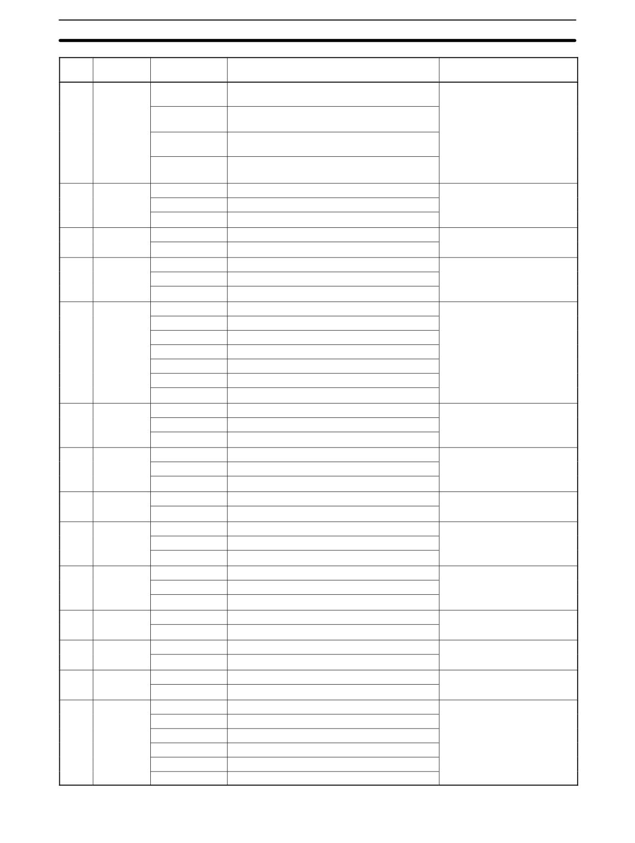
CPM2A/CPM2C Cycle Time and I/O Response Time
Section
8-2
Code
Mnemonic
ON execution
Conditions (T
op: min.; bottom: max.)
OFF execution time (µs)
time (µs)
65
PULS
38.4
Specifying a relative pulse for the set pulse out-
2.6
put via a word
46.6
Specifying a relative pulse for the set pulse out-
put via :DM
40.0
Specifying an absolute pulse for the set pulse
output via a word
48.1
Specifying an absolute pulse for the set pulse
output via :DM
66
SCL
37.9
Specifying a parameter word; constant to word
2.6
39.2
Specifying a parameter word; word to word
59.9
Specifying a parameter :DM ; :DM to :DM
67
BCNT
24.9
When counting 1 word
2.6
4.32 ms
When counting 2,048 words via :DM
68
BCMP
35.3
Comparing constant, results to word
2.6
38.3
Comparing word, results to word
58.1
Comparing :DM, results to :DM
69
STIM
25.7
Constant-set one-shot interrupt start
2.6
47.8
:DM-set one-shot interrupt start
25.9
Constant-set scheduled interrupt start
47.8
:DM-set scheduled interrupt start
34.0
Constant-set timer read
46.4
:DM-set timer read
10.6
Stopping timer
70
XFER
21.3
When transferring a constant to a word
2.6
23.8
When transferring a word to a word
1.52 ms
When transferring 2,048 words using :DM
71
BSET
13.8
When setting a constant to a word
2.6
14.3
When setting a word to a word
971.1
When setting :DM to 2,048 words
73
XCHG
14.5
Word → word
2.6
29.3
:DM → :DM
74
SLD
12.3
Shifting 1 word
2.6
23.9
Shifting 10 words
2.83 ms
Shifting 2,048 words using :DM
75
SRD
12.3
Shifting 1 word
2.6
23.9
Shifting 10 words
2.83 ms
Shifting 2,048 words using :DM
76
MLPX
16.8
When decoding word to word
2.6
46.1
When decoding :DM to :DM
77
DMPX
19.7
When encoding word to word
2.6
52.1
When encoding :DM to :DM
78
SDEC
19.8
When decoding word to word
2.6
48.3
When decoding :DM to :DM
80
DIST
18.7
When setting a constant to a word + a word
2.6
20.2
When setting a word to a word + a word
43.1
When setting :DM to :DM +:DM
31.0
When setting a constant to a stack
32.7
When setting a word to a stack
55.9
When setting :DM to a stack via :DM
529
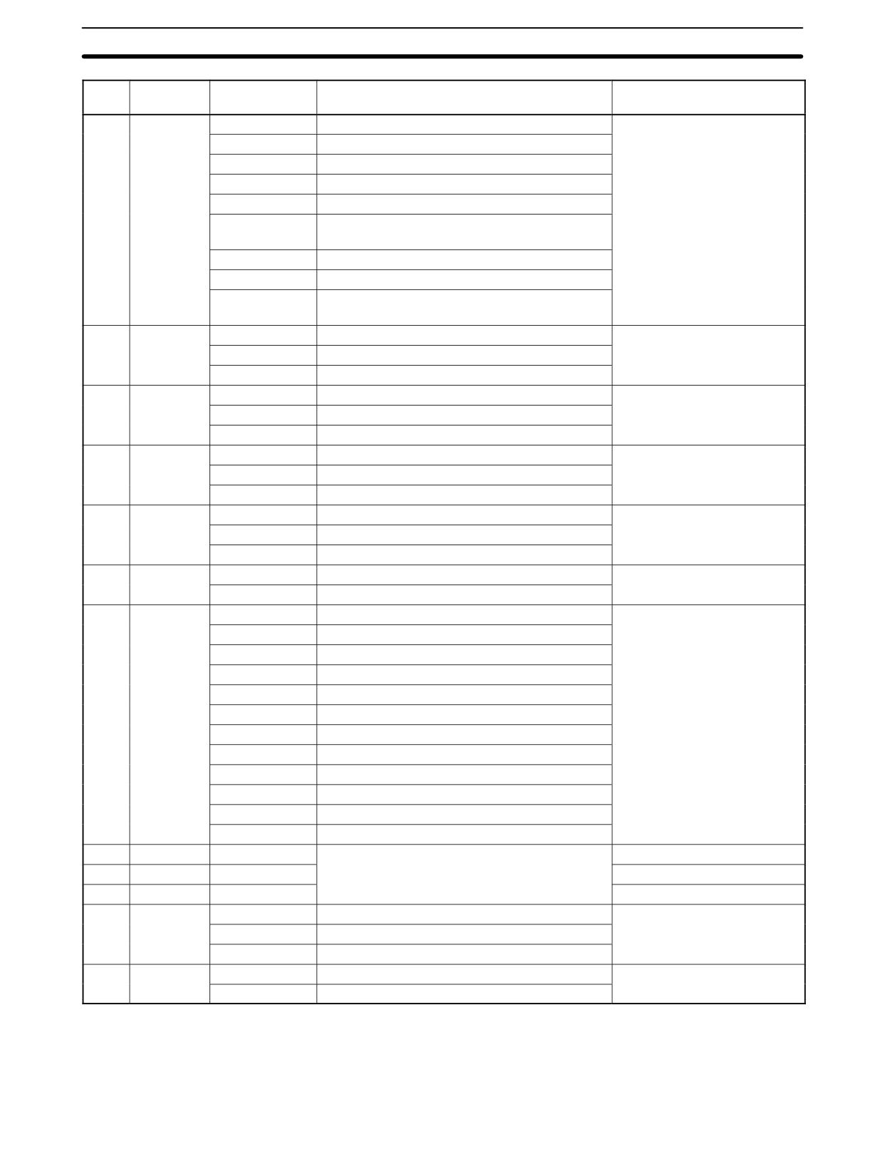
CPM2A/CPM2C Cycle Time and I/O Response Time
Section
8-2
Code
Mnemonic
ON execution
Conditions (T
op: min.; bottom: max.)
OFF execution time (µs)
time (µs)
81
COLL
21.5
When setting a constant + a word to a word
2.6
21.9
When setting a word + a word to a word
42.5
When setting :DM + :DM to :DM
31.5
When setting a word + constant to FIFO stack
32.0
When setting a word + word to FIFO stack
784.7
When setting a :DM + :DM to FIFO stack via
:DM
33.6
When setting a word + constant to LIFO stack
34.0
When setting a word + word to LIFO stack
57.1
When setting a :DM + :DM to LIFO stack via
:DM
82
MOVB
17.3
When transferring a constant to a word
2.6
18.0
When transferring from one word to another
41.7
When transferring :DM to :DM
83
MOVD
13.8
When transferring a constant to a word
2.6
16.2
When transferring from one word to another
38.1
When transferring :DM to :DM
84
SFTR
22.8
Shifting 1 word
2.6
24.3
Shifting 10 words
1.15 ms
Shifting 2,048 words using :DM
85
TCMP
27.5
Comparing constant to word-set table
2.6
28.0
Comparing word to word-set table
48.3
Comparing :DM to :DM-set table
86
ASC
19.1
Word → word
2.6
52.2
:DM → :DM
89
INT
22.1
Set masks via word
2.6
30.1
Set masks via :DM
18.4
Clear interrupts via word
26.4
Clear interrupts via :DM
17.2
Read mask status via word
24.1
Read mask status via :DM
23.1
Change counter SV via word
31.1
Change counter SV via :DM
10.7
Mask all interrupts via word
10.7
Mask all interrupts via :DM
11.0
Clear all interrupts via word
11.0
Clear all interrupts via :DM
91
SBS
10.8
Any
2.6
92
SBN
---
0.76
93
RET
6.2
1.0
97
IORF
16.8
Refreshing IR 000
2.8
130.7
Refreshing one input word
110.7
Refreshing one output word
99
MCRO
26.1
With word-set I/O operands
2.6
42.3
With :DM-set I/O operands
530
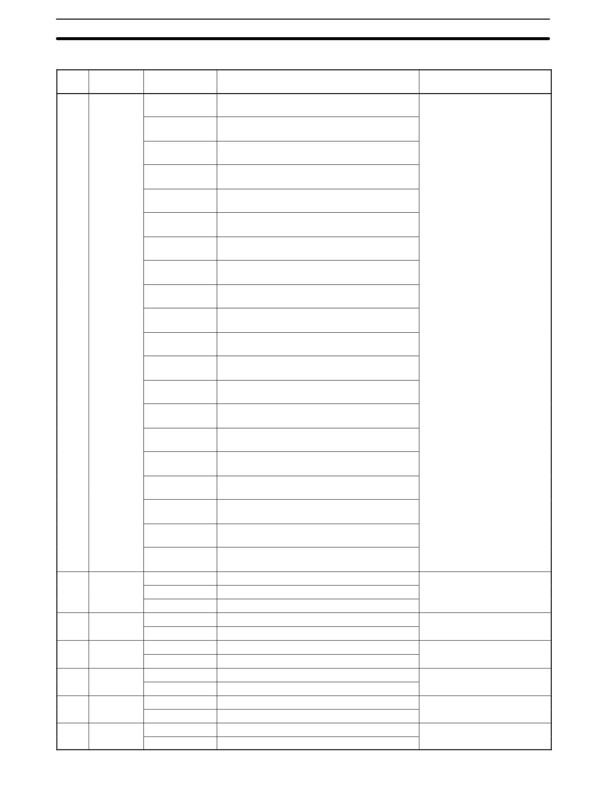
CPM2A/CPM2C Cycle Time and I/O Response Time
Section
8-2
Expansion Instructions without Default Function Codes
Code
Mnemonic
ON execution
Conditions (Top: min.; bottom: max.)
OFF execution time (µs)
time (µs)
---
ACC
66.5
When specifying a word in independent mode
2.6
and CW/CCW mode
92.1
When specifying :DM in independent mode
and CW/CCW mode
66.2
When specifying a word in independent mode
and Feed/Dir mode
92.2
When specifying :DM in independent mode
and Feed/Dir mode
65.5
When executing the word designation in CW
continuous mode and CW/CCW mode
75.0
When executing the :DM designation in CW
continuous mode and CW/CCW mode
45.4
When changing the word designation in CW
continuous mode and CW/CCW mode
53.8
When changing the :DM designation in CW
continuous mode and CW/CCW mode
65.5
When executing the word designation in CCW
continuous mode and CW/CCW mode
75.0
When executing the :DM designation in CCW
continuous mode and CW/CCW mode
45.5
When changing the word designation in CCW
continuous mode and CW/CCW mode
53.6
When changing the :DM designation in CCW
continuous mode and CW/CCW mode
65.0
When executing the word designation in CW
continuous mode and Feed/Dir mode
74.5
When executing the :DM designation in CW
continuous mode and Feed/Dir mode
45.4
When changing the word designation in CW
continuous mode and Feed/Dir mode
53.5
When changing the :DM designation in CW
continuous mode and Feed/Dir mode
65.4
When executing the word designation in CCW
continuous mode and Feed/Dir mode
74.8
When executing the :DM designation in CCW
continuous mode and Feed/Dir mode
45.5
When changing the word designation in CCW
continuous mode and Feed/Dir mode
53.6
When changing the :DM designation in CCW
continuous mode and Feed/Dir mode
---
AVG
23.2
Average for 1 cycle (constant designation)
3.2
23.9
Average for 1 cycle (word designation)
84.2
Average for 64 cycles (:DM designation)
---
FCS
27.6
Adding one word and outputting to word
2.6
592.3
Adding 999 words and outputting to :DM
---
HEX
25.8
Word → Word
2.6
72.2
:DM → :DM
---
HMS
30.7
When converting word to word
2.6
45.0
When converting :DM to :DM
---
MAX
21.9
Searching one word and outputting to word
2.6
713.9
Searching 999 words and outputting to :DM
---
MIN
21.9
Searching one word and outputting to word
2.6
713.9
Searching 999 words and outputting to :DM
531
CPM2A/CPM2C Cycle Time and I/O Response Time
Section
8-2
Code
Mnemonic
ON execution
Conditions (T
op: min.; bottom: max.)
OFF execution time (µs)
time (µs)
---
NEG
12.0
Converting constant to word
3.0
12.8
Converting word to word
28.3
Converting :DM to :DM
---
PID
392.5
Initializing word to word
3.3
418.8
Initializing :DM to :DM
29.3
Sampling word to word
58.7
Sampling :DM to :DM
---
PWM
30.3
Constant for pulse width ratio
2.6
43.4
Word for pulse width ratio
46.0
:DM for pulse width ratio
---
SCL2
35.1
Parameter word designation, word to word
2.6
59.3
Parameter :DM designation, :DM to :DM
---
SCL3
37.1
Parameter word designation, word to word
2.6
62.3
Parameter :DM designation, :DM to :DM
---
SEC
29.8
Converting from word to word
2.6
44.0
Converting from :DM to :DM
---
SRCH
28.9
Searching one word and outputting to a word
2.6
1.40 ms
:DM specification, searching 2,048 words and
outputting to :DM
---
STUP
3.42 ms
Constant specification, executed first scan
2.6
34.1
Constant specification, executed second scan
or later
3.44 ms
:DM specification, executed first scan
39.8
:DM specification, executed second scan or
later
---
SUM
22.8
Word added and output to word
2.6
1.44 ms
:DM specification, 999 bytes added and output
to :DM
---
SYNC
34.6
Constant ratio specification, when executed
2.6
35.3
Word ratio specification, when executed
42.5
:DM ratio specification, when executed
25.3
Word ratio specification, when changed
32.6
:DM ratio specification, when changed
---
TIML
Reset
IL
JMP
12.8
Normal execution, constant specification
17.9
17.5
8.1
13.5
Interrupt execution, constant specification
25.7
25.5
8.1
---
TMHH
Reset
IL
JMP
12.3
Normal execution, constant specification
15.6
15.1
7.4
12.7
Interrupt execution, constant specification
17.2
16.9
9.1
12.7
Normal execution, :DM specification
23.6
23.3
7.7
13.6
Interrupt execution, :DM specification
25.1
24.7
9.1
---
ZCP
9.4
Comparing a constant to a constant range and
2.6
output to word
11.8
Comparing a word to a word range and output
to word
33.4
Comparing :DM to :DM and output to :DM
---
ZCPL
19.5
Comparing a word to a word range
2.6
45.2
Comparing :DM to :DM
532
SRM1(-V2) Cycle Time and I/O Response Time
Section
8-3
8-3
SRM1(-V2) Cycle Time and I/O Response Time
8-3-1
The SRM1(-V2) Cycle
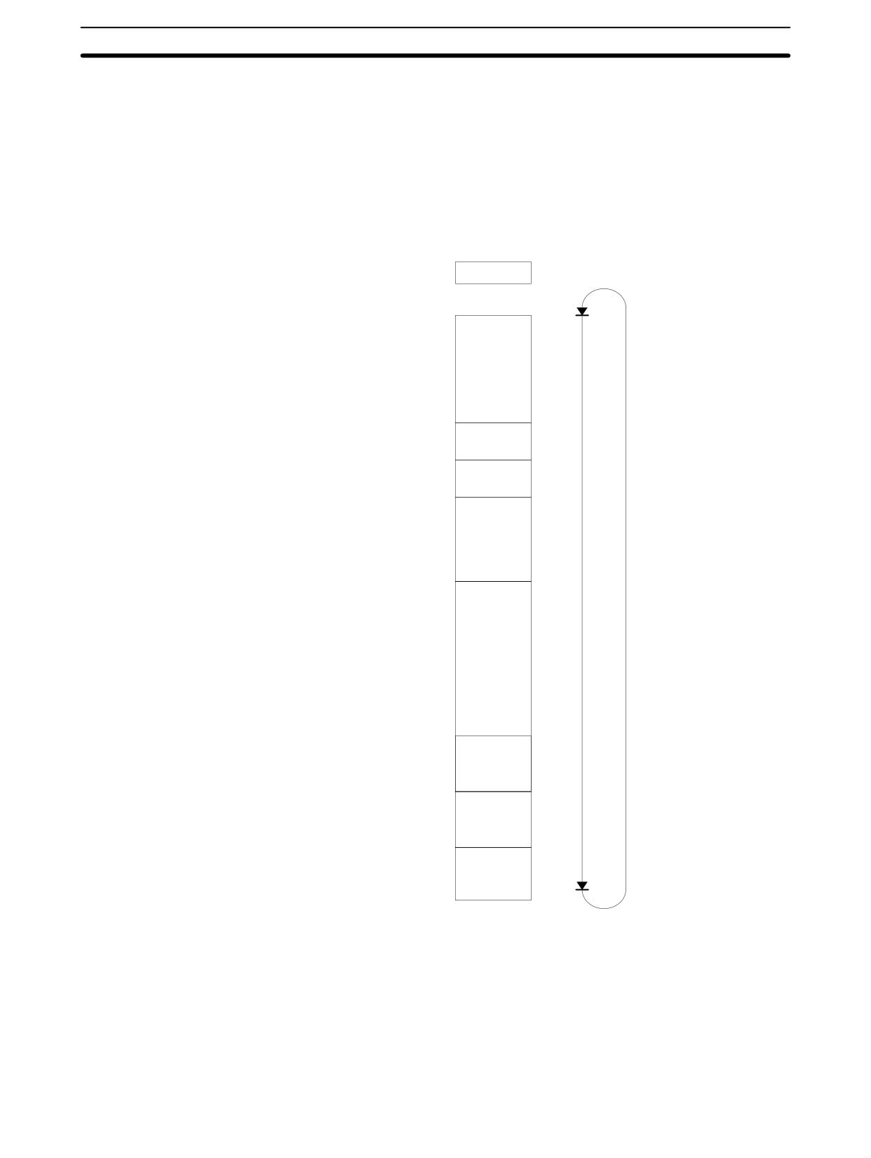
The overall flow of SRM1(-V2) operation is as shown in the following flowchart.
Initialization
Overseeing
processes
CompoBus/S
end wait
Input
refreshing
Program
execution
Cycle
time
Cycle time
processing
Output re-
freshing
RS-232C
servicing
Peripheral
port ser-
vicing
Note
1. The cycle time can be read using Programming Devices.
2. Cycle time maximum and current cycle time are stored in AR 14 and AR 15.
3. Change to processing will cause cycle times to change therefore the calcu-
lated values and actual values (for cycle time) will no always match.
533
SRM1(-V2) Cycle Time and I/O Response Time
Section
8-3
8-3-2
SRM1(-V2) Cycle Time
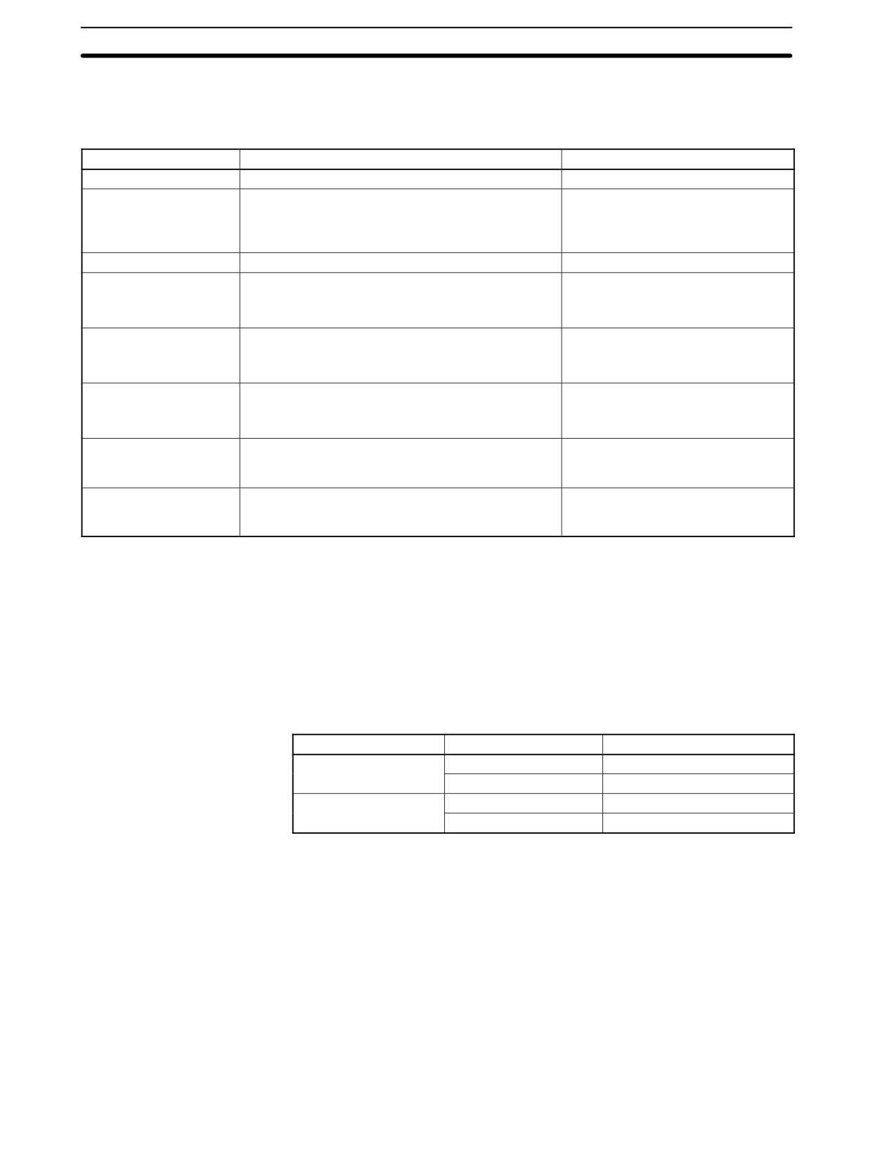
The processes involved in a single SRM1(-V2) cycle are shown in the following
table, and their respective processing times are explained.
Process
Content
Time requirements
Overseeing
Setting cycle watchdog timer, UM check, etc.
0.18 ms
CompoBus/S end wait
Waiting for CompoBus/S processing to finish
CompoBus/S communications re-
sponse time - Overseeing time -
RS-232C port servicing time - periph-
eral port servicing time
Input refreshing
Input information is read to input bits.
0.02 ms
Program execution
User program is executed.
Total time for executing instructions.
(Varies according to content of user’s
Refer to 8-3-6 SRM1(-V2) Instruction Execution
program.)
Times.
Cycle time calculation
Standby until set time, when minimum cycle time is
Almost instantaneous, except for
set in DM 6619 of PC Setup.
standby processing.
Calculation of cycle time.
Output refreshing
Output information (results of executing program) is
0.05 ms
written to output bits.
CompoBus/S communications are started.
RS-232C port servicing
Devices connected to RS-232C port serviced.
5% or less of cycle time, but always
between 0.55 and 131 ms
(Set in DM 6616.)
Peripheral port servicing
Devices connected to peripheral port serviced.
5% or less of cycle time, but always
between 0.55 and 131 ms
(Set in DM 6617.)
Minimum Cycle Time
In SRM1(-V2) PCs, CompoBus/S communications are started after the output
refresh is completed. As a result, when the overseeing time plus the RS-232C
port servicing time plus the peripheral port servicing time is shorter than the
CompoBus/S communications response time, processing is placed on stand-by
until CompoBus/S communications are completed.
The minimum cycle time therefore is the the CompoBus/S communications re-
sponse time plus the program execution time plus the input refresh time plus the
output refresh time. The CompoBus/S communications response time depends
on the “maximum number of nodes” and “communications mode” settings, as
follows:
Max. number of nodes
Communications mode
CompoBus/S response time
32
High-speed mode
0.8 ms
Long-distance mode
6.0 ms
16
High-speed mode
0.5 ms
Long-distance mode
4.0 ms
Note The maximum number of nodes and communications mode are set in the PC
Setup (DM 6603).
534
SRM1(-V2) Cycle Time and I/O Response Time
Section
8-3
Cycle Time and Operations
The effects of the cycle time on SRM1(-V2) operations are as shown below.
When a long cycle time is affecting operation, either reduce the cycle time or im-
prove responsiveness with interrupt programs.
Cycle time
Operation conditions
10 ms or longer
TIMH(15) may be inaccurate when TC 004 through TC 127 are used (operation will be normal for
TC 000 through TC 003).
20 ms or longer
Programming using the 0.02-second Clock Bit (SR 25401) may be inaccurate.
100 ms or longer
TIM may be inaccurate. Programming using the 0.1-second Clock Bit (SR 25500) may be inaccu-
rate. A CYCLE TIME OVER error is generated (SR 25309 will turn ON). See note 1.
120 ms or longer
The FALS 9F monitoring time SV is exceeded. A system error (FALS 9F) is generated, and opera-
tion stops. See note 2.
200 ms or longer
Programming using the 0.2-second Clock Bit (SR 25501) may be inaccurate.
Note
1. The PC Setup (DM 6655) can be used to disable detection of CYCLE TIME
OVER error.
2. The cycle monitoring time can be changed in the PC Setup (DM 6618).
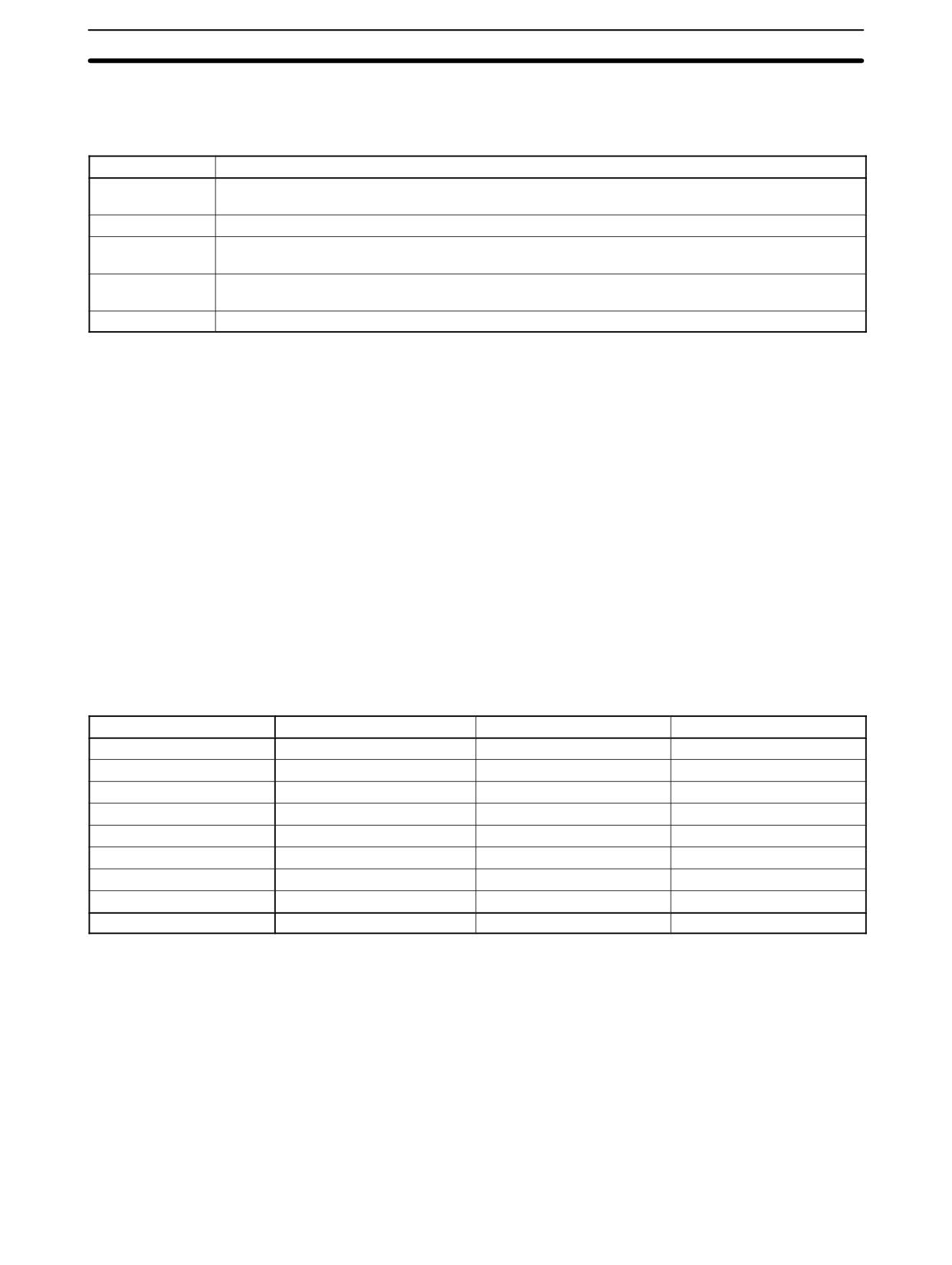
Cycle Time Example
The following is an example of a cycle time calculation.
The operating conditions are assumed to be as follows:
User’s program:500 instructions (consists of only LD and OUT)
Cycle time:
Variable (no minimum set)
RS-232C port: Not used.
Max. nodes:
32 nodes and high-speed communications mode
(CompoBus/S communication response time = 0.8 ms)
Peripheral:
0.7 ms
The average processing time for a single instruction in the user’s program is as-
sumed to be 1.16 µs. The cycle times are as shown in the following table.
Process
Calculation method
Peripheral port used
Peripheral port not used
1. Overseeing
Fixed
0.18 ms
0.18 ms
2. CompoBus/S end wait
See previous page.
0.00 ms
0.62 ms
3. Input refresh
Fixed
0.02 ms
0.02 ms
4. Program execution
1.16 × 500 (µs)
0.8 ms
0.8 ms
5. Cycle time calculation
Negligible
0.00 ms
0.00 ms
6. Output refresh
0.01 × 1 + 0.005 × 1 (µs)
0.05 ms
0.05 ms
7. RS-232C port servicing
Not required
0.00 ms
0.00 ms
8. Peripheral port servicing
5% of cycle time
0.7 ms
0.00 ms
Cycle time
(1) + (2) + (3) + ...+ (8)
1.75 ms
1.67 ms
Note
1. The cycle time can be read from the PC via a Programming Device.
2. The maximum and current cycle time are stored in AR 14 and AR 15.
3. The cycle time can vary with actual operating conditions and will not neces-
sarily agree precisely with the calculated value.
4. When the peripheral port is used, there is no CompoBus/S end wait time as it
is always 0 or less.
5. CompoBus/S end wait time = 0.8 - 0.18 - 0 - 0 = 0.62 (CompoBus/S com-
munication response time - Overseeing - RS-232C port servicing time -
peripheral port servicing time.
535
SRM1(-V2) Cycle Time and I/O Response Time
Section
8-3
8-3-3
I/O Response Time
The I/O response time is the time it takes after an input signal has been received
(i.e., after an input bit has turned ON) for the PC to check and process the in-
formation and to output a control signal (i.e., to output the result of the proces-
sing to an output bit).
CompoBus/S communications are started when the SRM1(-V2) input refresh fi-
nishes. The ON/OFF status is read from the Input Terminals during the input re-
fresh and the ON/OFF status is output to the Output Terminal during the output
refresh. Accordingly, the SRM1(-V2) I/O response time varies according to the
cycle time and CompoBus/S communications cycle status or I/O timing.
Example calculations of the I/O response time are provided next.
Minimum I/O Response Time
Minimum I/O response time =
Input ON delay + Output ON delay + CompoBus/S communications cycle time +
SRM1(-V2) cycle time
Cycle time
SRM1(-V2) cycle
Communications
CompoBus/S
response time
cycle time
Input
delay
Input on Slave
Output
Output on Slave
delay
Maximum I/O Response Time
Maximum I/O response time =
Input ON delay + Output ON delay + CompoBus/S communications cycle time +
SRM1(-V2) cycle time x 2
Cycle
time
SRM1(-V2) cycle
Communications
CompoBus/S
response time
cycle time
Input
delay
Input on Slave
Output
Output on Slave
delay
536
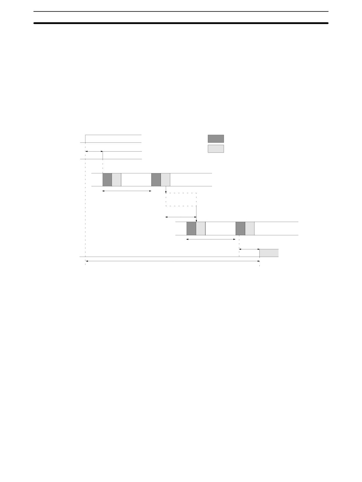
SRM1(-V2) Cycle Time and I/O Response Time
Section
8-3
8-3-4
One-to-one PC Link I/O Response Time
When two SRM1s are linked in a 1:1 PC Link, the I/O response time is the time
required for an input executed at one of the SRM1s to be output to the other
SRM1 by means of 1:1 PC Link communications.
Minimum I/O Response Time The SRM1(-V2) responds most quickly under the following circumstances:
1, 2, 3...
1. The SRM1(-V2) receives an input signal just prior to the I/O refresh phase of
the cycle.
2. The Master’s communications servicing occurs just as the Master-to-Slave
transmission begins.
3. The Slave’s communications servicing occurs just after the transmission is
completed.
Input
I/O refresh
point
Input ON delay (8 ms)
Overseeing, communica-
tions, etc.
Input
bit
Program
execution
Master’s cycle time (10 ms)
Master to
Slave
Transmission time (39 ms)
Program
execution
Output ON
Slave’s cycle time (15 ms)
delay (10 ms)
Output
point
Min. I/O response time = 8+10+39+15+10 = 82 ms
Maximum I/O Response Time The SRM1(-V2) takes the longest to respond under the following circum-
stances:
1, 2, 3...
1. The SRM1(-V2) receives an input signal just after the I/O refresh phase of
the cycle.
2. The Master’s communications servicing just misses the Master-to-Slave
transmission.
537
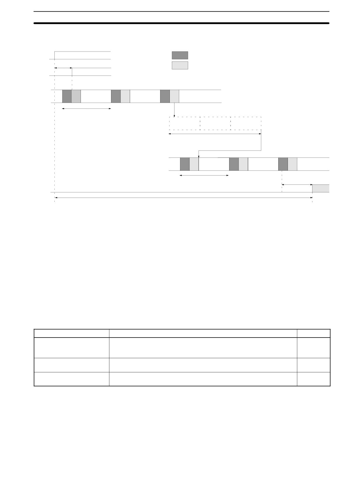
SRM1(-V2) Cycle Time and I/O Response Time
Section
8-3
3. The transmission is completed just after the Slave’s communications servic-
ing ends.
I/O refresh
Input
point
Input ON delay (8 ms)
Overseeing, communica-
tions, etc.
Input
bit
Program
Program
execution
execution
Master’s cycle time (10 ms)
Master to
Slave to
Master to
Slave
Master
Slave
Transmission time (39 ms × 3)
Program
Program
execution
execution
Output ON
Slave’s cycle time (15 ms)
delay (10 ms)
Output
point
Max. I/O response time = 8 + 10 × 2 + 39 × 3 + 15× 2 + 10 = 185 ms
8-3-5
Interrupt Processing Time
This section explains the processing times involved from the time an interrupt is
executed until the interrupt processing routine is called, and from the time an in-
terrupt processing routine is completed until returning to the initial location. This
explanation applies to input, interval timer interrupts.
1, 2, 3...
1. Source of interrupt
2. Wait for completion of interrupt-mask processing
3. Change to interrupt processing
4. Interrupt routing (CPM1A only)
5. Return to initial location
The table below shows the times involved from the generation of an interrupt sig-
nal until the interrupt processing routine is called, and from when the interrupt
processing routine is completed until returning to the original position.
Item
Contents
Time
Wait for completion of
This is the time during which interrupts are waiting until processing has
See below.
interrupt-mask processing
been completed. This situation occurs when a mask processes is
executed. It is explained below in more detail.
Change to interrupt
This is the time it takes to change processing to an interrupt.
15 µs
processing
Return
This is the time it takes, from execution of RET(93), to return to the proces-
15 µs
sing that was interrupted.
Mask Processing
Interrupts are masked during processing of the operations described below. Un-
til the processing is completed, any interrupts will remain masked for the indi-
cated times.
Generation and clearing of non-fatal errors:
When a non-fatal error is generated and the error contents are registered at
the SRM1(-V2), or when an error is being cleared, interrupts will be masked
for a maximum of 100 µs until the processing has been completed.
538
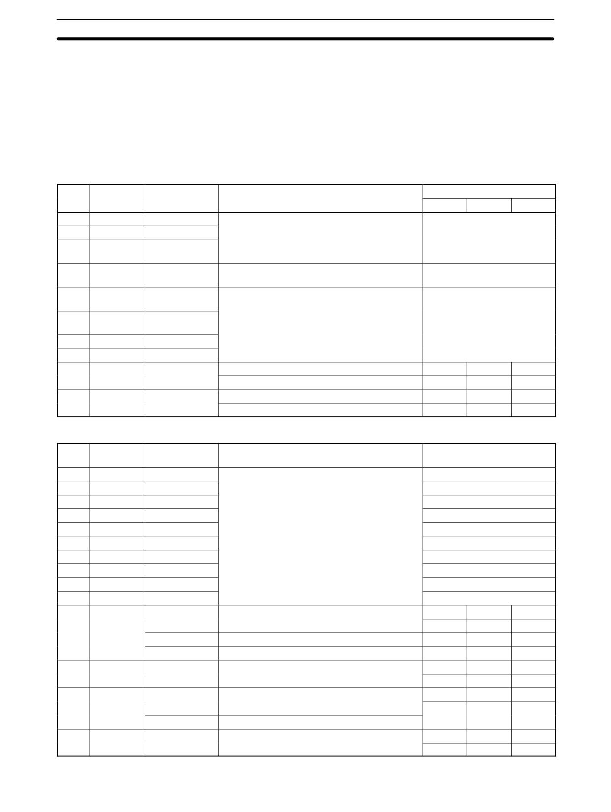
SRM1(-V2) Cycle Time and I/O Response Time
Section
8-3
Online editing:
Interrupts will be masked for a maximum of 600 ms (i.e.: editing DM 6144 to
DM 6655) when online editing is executed during operation. In addition, the
system processing may have to wait for a maximum of 170 µs during this
processing.
8-3-6
SRM1(-V2) Instruction Execution Times
The following table lists the execution times for SRM1(-V2) instructions.
Basic Instructions
Code
Mnemonic
ON execution
Conditions (Top: min.; bottom: max.)
OFF execution time (µs)
ti
me
(µs
)
RSET
IL
JMP
---
LD
0.97
Any
---
---
LD NOT
0.97
---
AND
0.77
---
AND NOT
---
OR
0.78
Any
---
---
OR NOT
---
AND LD
0.39
Any
---
---
OR LD
---
OUT
2.2
---
OUT NOT
---
SET
2.7
---
RSET
2.8
---
TIM
5.7
Constant for SV
9.3
9.1
3.5
:DM for SV
17.4
17.2
3.5
---
CNT
6.6
Constant for SV
8.0
3.6
3.8
:DM for SV
16.3
3.6
3.8
Special Instructions and Expansion Instructions
Code
Mnemonic
ON execution
Conditions (Top: min.; bottom: max.)
OFF execution time (µs)
time (µs)
00
NOP
0.20
Any
01
END
4.8
02
IL
2.5
1.4
03
ILC
1.9
1.9
04
JMP
2.2
1.3
05
JME
2.5
2.5
06
FAL
18.4
2.9
07
FALS
3.6
2.9
08
STEP
10.7
9.0
09
SNXT
5.9
4.1
10
SFT
14.5
Reset
IL
JMP
With 1-word shift register
11.0
1.4
1.4
21.0
With 10-word shift register
14.9
1.4
1.4
49.1
With 100-word shift register
30.8
1.4
1.4
11
KEEP
3.0
Any
Reset
IL
JMP
3.4
1.6
1.7
12
CNTR
14.8
Reset
IL
JMP
Constant for SV
9.1
6.6
6.5
23.2
:DM for SV
13
DIFU
6.7
Any
Shift
IL
JMP
5.8
5.2
1.3
539
SRM1(-V2) Cycle Time and I/O Response Time
Section
8-3
Code
Mnemonic
ON execution
Conditions (T
op: min.; bottom: max.)
OFF execution time (µs)
time (µs)
14
DIFD
6.4
Any
Shift
IL
JMP
5.8
5.7
1.3
15
TIMH
10.3
Reset
IL
JMP
Regular execution, constant for SV
14.1
13.9
7.0
10.9
Interrupt execution, constant for SV
15.6
15.4
8.5
10.3
Regular execution, :DM for SV
22.8
22.1
7.0
10.9
Interrupt execution, :DM for SV
23.9
23.6
8.5
16
WSFT
16.2
With 1-word shift register
2.9
23.0
With 10-word shift register
712.3
With 1,024-word shift register using :DM
17
ASFT*
18.6
Shifting a word
3.0
25.9
Shifting 10 words
865.7
Shifting 1,023 words via :DM
20
CMP
9.1
When comparing a constant to a word
3.0
9.9
When comparing two words
25.6
When comparing two :DM
21
MOV
9.1
When transferring a constant to a word
3.0
9.5
When transferring from one word to another
24.9
When transferring :DM to :DM
22
MVN
9.3
When transferring a constant to a word
3.0
9.8
When transferring from one word to another
25.1
When transferring :DM to :DM
23
BIN
17.2
When converting a word to a word
3.0
32.0
When converting :DM to :DM
24
BCD
15.8
When converting a word to a word
3.0
30.6
When converting :DM to :DM
25
ASL
9.9
When shifting a word
2.9
17.3
When shifting :DM
26
ASR
9.7
When shifting a word
3.0
17.2
When shifting :DM
27
ROL
8.5
When rotating a word
2.9
16.1
When rotating :DM
28
ROR
8.5
When rotating a word
2.9
16.1
When rotating :DM
29
COM
10.5
When inverting a word
3.0
17.7
When inverting :DM
30
ADD
15.9
Constant + word → word
3.1
16.4
Word + word → word
39.5
:DM + :DM → :DM
31
SUB
15.6
Constant - word → word
3.0
16.3
Word - word → word
38.6
:DM - :DM → :DM
32
MUL
29.7
Constant word → word
3.0
28.5
Word word → word
51.6
:DM :DM → :DM
33
DIV
27.2
Word ÷ constant → word
2.9
28.5
word ÷ word → word
53.1
:DM ÷ :DM → :DM
540
SRM1(-V2) Cycle Time and I/O Response Time
Section
8-3
Code
Mnemonic
ON execution
Conditions (T
op: min.; bottom: max.)
OFF execution time (µs)
time (µs)
34
ANDW
14.3
Constant Ɠ word → word
2.9
15.2
Word Ɠ word → word
37.3
:DM Ɠ :DM → :DM
35
ORW
14.3
Constant V word → word
2.9
15.2
Word V word → word
37.3
:DM V :DM → :DM
36
XORW
14.3
Constant V word → word
2.9
15.2
Word V word → word
37.3
:DM V :DM → :DM
37
XNRW
14.3
Constant V word → word
2.9
15.2
Word V word → word
37.3
:DM V :DM → :DM
38
INC
9.9
When incrementing a word
2.9
17.3
When incrementing :DM
39
DEC
10.2
When decrementing a word
2.9
17.4
When decrementing :DM
40
STC
3.5
Any
2.9
41
CLC
3.0
2.9
46
MSG
11.3
With message in words
2.9
19.4
With message in :DM
47
RXD*
39.1
Word specification, 1 byte input
2.9
116.8
:DM specification, 256 bytes input
48
TXD*
31.3
Word specification, 1 byte input (RS-232C)
2.9
266.5
:DM specification, 256 bytes input (RS-232C)
26.7
Word specification, 1 byte input (Host Link)
34.0
:DM specification, 256 bytes input (Host Link)
50
ADB
16.8
Constant + word → word
3.0
17.6
Word + word → word
39.9
:DM + :DM → :DM
51
SBB
17.0
Constant - word → word
3.0
17.8
Word - word → word
40.2
:DM - :DM → :DM
52
MLB
19.1
Constant word → word
3.0
20.1
Word word → word
43.5
:DM :DM → :DM
53
DVB
19.5
Word ÷ constant → word
3.0
20.4
Word ÷ word → word
43.7
:DM ÷ :DM → :DM
54
ADDL
26.7
Word + word → word
3.0
49.9
:DM + :DM → :DM
55
SUBL
26.8
Word - word → word
3.0
49.9
:DM - :DM → :DM
56
MULL
81.4
Word word → word
3.0
106.2
:DM :DM → :DM
57
DIVL
76.9
Word ÷ word → word
3.0
101.8
:DM ÷ :DM → :DM
60
CMPL
16.9
Comparing words
2.9
32.9
Comparing :DM
541
SRM1(-V2) Cycle Time and I/O Response Time
Section
8-3
Code
Mnemonic
ON execution
Conditions (T
op: min.; bottom: max.)
OFF execution time (µs)
time (µs)
66
SCL*
69.5
Word specification
3.0
91.5
:DM specification
67
BCNT*
26.9
Counting a word
3.0
2.29 ms
Counting 6,656 words via :DM
68
BCMP*
41.4
Comparing constant, results to word
3.0
41.9
Comparing word, results to word
64.5
Comparing :DM, results to :DM
69
STIM*
34.7
Word specification, one-shot timer start
3.0
49.5
:DM specification, one-shot timer start
35.3
Word specification, scheduled interrupt start
50.0
:DM specification, scheduled interrupt start
33.9
Words specification, timer read
49.5
:DM specification timer read
11.4
Word specification, timer stop
70
XFER
22.9
When transferring a constant to a word
3.0
24.0
When transferring a word to a word
902.0
When transferring 1,024 words using :DM
71
BSET
15.2
When setting a constant to 1 word
3.0
15.7
When setting word constant to 10 words
565.2
When setting :DM to 1,024 words
73
XCHG
16.2
Word → word
3.1
31.5
:DM → :DM
74
SLD
13.6
Shifting 1 word
3.0
26.7
Shifting 10 word
1.54 ms
Shifting 1024 words using :DM
75
SRD
13.6
Shifting 1 word
3.0
26.6
Shifting 10 word
1.54 ms
Shifting 1,024 words using :DM
76
MLPX
25.5
When decoding word to word
3.0
48.9
When decoding :DM to :DM
77
DMPX
35.1
When encoding word to word
3.0
58.1
When encoding :DM to :DM
78
SDEC
26.8
When decoding word to word
2.9
49.9
When decoding :DM to :DM
80
DIST
21.3
When setting a constant to a word + a word
3.0
21.9
When setting a word to a word + a word
45.7
When setting :DM to :DM +:DM
34.3
When setting a constant to a stack
35.3
When setting a word to a stack
59.3
When setting :DM to a stack via :DM
542
SRM1(-V2) Cycle Time and I/O Response Time
Section
8-3
Code
Mnemonic
ON execution
Conditions (T
op: min.; bottom: max.)
OFF execution time (µs)
time (µs)
81
COLL
21.4
When setting a constant + a word to a word
3.0
21.8
When setting a word + a word to a word
44.9
When setting :DM + :DM to :DM
34.0
When setting a word + constant to FIFO stack
33.9
When setting a word + word to FIFO stack
892.0
When setting a :DM + :DM to
FIFO stack via :DM
35.4
When setting a word + constant to LIFO stack
36.1
When setting a word + word to LIFO stack
60.5
When setting a :DM + :DM to
LIFO stack via :DM
82
MOVB
18.2
When transferring a constant to a word
3.0
19.0
When transferring one word to another
42.1
When transferring :DM to :DM
83
MOVD
16.3
When transferring a constant to a word
2.9
17.6
When transferring one word to another
39.9
When transferring :DM to :DM
84
SFTR
21.0
Shifting 1 word
3.0
26.9
Shifting 10 word
718.5
Shifting 1,024 words using :DM
85
TCMP
30.0
Comparing constant to word-set table
3.0
30.7
Comparing word to word-set table
53.1
Comparing :DM to :DM-set table
86
ASC
30.0
Word → word
3.0
53.7
:DM → :DM
91
SBS
13.2
Any
3.0
92
SBN
---
1.3
93
RET
7.8
1.3
99
MCRO
26.8
With word-set I/O operands
3.0
43.5
With :DM-set I/O operands
Note Those instructions marked with an asterisk are expansion instructions.
Expansion Instructions without Default Function Codes
Code
Mnemonic
ON execution
Conditions (Top: min.; bottom: max.)
OFF execution time (µs)
time (µs)
---
FCS
23.4
Adding one word and outputting to word
3.0
643.7
Adding 999 words and outputting to :DM
---
HEX
43.6
DM → DM
3.0
73.5
:DM → :DM
---
NEG
46.0
Converting constant to word
3.0
48.0
Converting word to word
65.5
Converting :DM to :DM
---
PID
420.0
Initializing word to word
3.0
452.0
Initializing :DM to :DM
63.0
Sampling word to word
84.5
Sampling :DM to :DM
---
STUP
51.2
Transferring constant to word
3.0
58.2
Transferring word to word
543

SRM1(-V2) Cycle Time and I/O Response Time
Section
8-3
Code
Mnemonic
ON execution
Conditions (T
op: min.; bottom: max.)
OFF execution time (µs)
time (µs)
---
ZCP
45.0
Comparing a word to a constant range
3.0
46.5
Comparing a word to a word range
69.0
Comparing :DM to :DM
544
SECTION 9
Troubleshooting
This section describes how to diagnose and correct the hardware and software errors that can occur during PC operation.
9-1
Introduction
546
9-2
Programming Console Operation Errors
546
9-3
Programming Errors
547
9-4
User-defined Errors
548
9-5
Operating Errors
549
9-5-1
Non-fatal Errors
549
9-5-2
Fatal Errors
550
9-5-3
Other Errors
550
9-6
Error Log
551
9-7
Host Link Errors
553
9-8
Troubleshooting Flowcharts
553
545

Programming Console Operation Errors
Section
9-2
9-1
Introduction
PC errors can be divided broadly into the following four categories:
1, 2, 3...
1. Program Input Errors
These errors occur when inputting a program or attempting an operation
used to prepare the PC for operation.
2. Programming Errors
These errors will occur when the program is checked using the Program
Check operation.
3. User-defined Errors
There are three instructions that the user can use to define his own errors or
messages. The instructions will be executed when a particular condition
(defined by the user) has occurred during operation.
4. Operating Errors
These errors occur after program execution has been started.
a) Non-fatal Operating Errors
PC operation and program execution will continue after one or more of
these errors have occurred.
b) Fatal Operating Errors
PC operation and program execution will stop and all outputs from the
PC will be turned OFF when any of these errors have occurred.
The PC’s indicators will indicate when a PC error has occurred and an error mes-
sage or code will be displayed on the Programming Console or host computer if
one is connected. The error code is also contained in SR 25300 to SR 25307.
For the most recent errors, both the type of error and time of occurrence will be
recorded in the PC’s error log area. Details are provided starting on page 551.
There are flags and other information provided in the SR and AR areas that can
be used in troubleshooting. Refer to Section 3 Memory Areas for lists of these.
Note
In addition to the errors described above, communications errors can occur
when the PC is part of a Host Link System. Refer to page 553 for details.
9-2
Programming Console Operation Errors
The following error messages may appear when performing operations on the
Programming Console. Correct the error as indicated and continue with the op-
eration. The asterisks in the displays shown below will be replaced with numeric
data, normally an address, in the actual display. Refer to the Ladder Support
Software Operation Manual, SYSMAC Support Software Operation Manual: C-
series PCs, or Data Access Console Operation Manual for errors that may ap-
pear when operating the SSS or a Data Access Console.
Message
Meaning and appropriate response
REPL ROM
An attempt was made to write to write-protected memory. Set bits
00 to 03 of DM 6602 to “0.”
PROG OVER
The instruction at the last address in memory is not NOP(00). Erase
all unnecessary instructions at the end of the program.
ADDR OVER
An address was set that is larger than the highest memory address
in Program Memory. Input a smaller address.
SET DATA
FALS 00 has been input, and “00” cannot be input. Re-input the
ERR
data.
I/O NO. ERR
A data area address has been designated that exceeds the limit of
the data area, e.g., an address is too large. Confirm the
requirements for the instruction and re-enter the address.
546
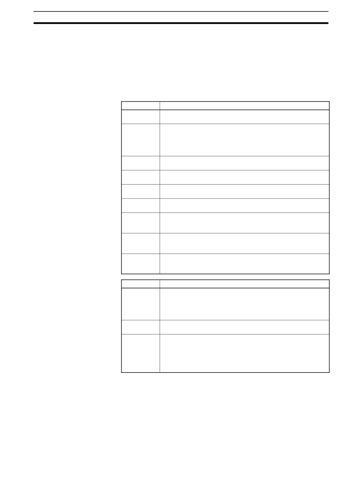
Programming Errors
Section
9-3
9-3
Programming Errors
These errors in program syntax will be detected when the program is checked
using the Program Check operation.
Three levels of program checking are available. The desired level must be
designated to indicate the type of errors that are to be detected. The follow-
ing table provides the error types, displays, and explanations of all syntax
errors. Check level 0 checks for type A, B, and C errors; check level 1, for
type A and B errors; and check level 2, for type A errors only.
Level A Errors
Message
Meaning and appropriate response
?????
The program has been damaged, creating a non-existent function
code. Re-enter the program.
CIRCUIT
The number of logic blocks and logic block instructions does not
ERR
agree, i.e., either LD or LD NOT has been used to start a logic
block whose execution condition has not been used by another
instruction, or a logic block instruction has been used that does not
have the required number of logic blocks. Check your program.
OPERAND
A constant entered for the instruction is not within defined values.
ERR
Change the constant so that it lies within the proper range.
NO END
There is no END(01) in the program. Write END(01) at the final
INSTR
address in the program.
LOCN ERR
An instruction is in the wrong place in the program. Check
instruction requirements and correct the program.
JME
A JME(05) instruction is missing for a JMP(04) instruction. Correct
UNDEFD
the jump number or insert the proper JME(05) instruction.
DUPL
The same jump number or subroutine number has been used twice.
Correct the program so that the same number is only used once for
each.
SBN
The SBS(91) instruction has been programmed for a subroutine
UNDEFD
number that does not exist. Correct the subroutine number or
program the required subroutine.
STEP ERR
STEP(08) with a section number and STEP(08) without a section
number have been used incorrectly. Check STEP(08) programming
requirements and correct the program.
Level B Errors
Message
Meaning and appropriate response
IL-ILC ERR
IL(02) and ILC(03) are not used in pairs. Correct the program so
that each IL(02) has a unique ILC(03). Although this error message
will appear if more than one IL(02) is used with the same ILC(03),
the program will be executed as written. Make sure your program is
written as desired before proceeding.
JMP-JME
JMP(04) and JME(05) are not used in pairs. Make sure your
ERR
program is written as desired before proceeding.
SBN-RET
If the displayed address is that of SBN(92), two different
ERR
subroutines have been defined with the same subroutine number.
Change one of the subroutine numbers or delete one of the
subroutines. If the displayed address is that of RET(93), RET(93)
has not been used properly. Check requirements for RET(93) and
correct the program.
547

User-defined Errors
Section
9-4
Level C Errors
Message
Meaning and appropriate response
COIL DUPL
The same bit is being controlled (i.e., turned ON and/or OFF) by
more than one instruction (e.g., OUT, OUT NOT, DIFU(13),
DIFD(14), KEEP(11), SFT(10)). Although this is allowed for certain
instructions, check instruction requirements to confirm that the
program is correct or rewrite the program so that each bit is
controlled by only one instruction.
JMP
JME(05) has been used with no JMP(04) with the same jump
UNDEFD
number. Add a JMP(04) with the same number or delete the
JME(05) that is not being used.
SBS
A subroutine exists that is not called by SBS(91). Program a
UNDEFD
subroutine call in the proper place, or delete the subroutine if it is
not required.
!
Caution Expansion instructions (those assigned to function codes 17, 18, 19, 47, 48, 60
to 69, 87, 88, and 89) are not subject to program checks. Program checks also
do not cover DM 1024 to DM 6143 for PCs that do not support this part of the DM
area. Data will not be written even if these areas are specified and data read from
these areas will always be “0000.”
9-4
User-defined Errors
There are four instructions that the user can use to define his own errors or mes-
sages. These instructions are used to send messages to the Programming Con-
sole connected to the PC, cause a non-fatal or a fatal error.
MESSAGE - MSG(46)
MSG(46) is used to display a message on the Programming Console. The mes-
sage, which can be up to 16 characters long, is displayed when the instruction’s
execution condition is ON. Refer to page 493 for details.
FAL(06) is an instruction that causes a non-fatal error. Refer to page 381 for de-
FAILURE ALARM - FAL(06)
tails. The following will occur when an FAL(06) instruction is executed:
1, 2, 3...
1. The ERR/ALM indicator on the CPU Unit will flash. PC operation will contin-
ue.
2. The instruction’s 2-digit BCD FAL number (01 to 99) will be written to
SR 25300 to SR 25307.
3. The FAL number will be recorded in the PC’s error log area. The time of oc-
currence will also be recorded in CPM2A PCs and CPM2C PCs that are
equipped with an internal clock.
The FAL numbers can be set arbitrarily to indicate particular conditions. The
same number cannot be used as both an FAL number and an FALS number.
To clear an FAL error, correct the cause of the error, execute FAL 00, and then
clear the error using the Programming Console.
FALS(07) is an instruction that causes a fatal error. Refer to page 381 for details.
SEVERE FAILURE ALARM -
FALS(07)
The following will occur when an FALS(07) instruction is executed:
1, 2, 3...
1. Program execution will be stopped and outputs will be turned OFF.
2. The ERR/ALM indicator on the CPU Unit will be lit.
3. The instruction’s 2-digit BCD FALS number (01 to 99) will be written to
SR 25300 to SR 25307.
4. The FALS number will be recorded in the PC’s error log area. The time of
occurrence will also be recorded in CPM2A PCs and CPM2C PCs that are
equipped with an internal clock.
The FALS numbers can be set arbitrarily to indicate particular conditions. The
same number cannot be used as both an FAL number and an FALS number.
To clear an FALS error, switch the PC to PROGRAM Mode, correct the cause of
the error, and then clear the error using the Programming Console.
548

Operating Errors
Section
9-5
9-5
Operating Errors
There are two kinds of operating errors, non-fatal and fatal. PC operation will
continue after a non-fatal error occurs, but operation will be stopped if a fatal
error occurs.
!
Caution Investigate all errors, whether fatal or not. Remove the cause of the error as
soon as possible and restart the PC. Refer to the CPM1 Operation Manual,
CPM2A Operation Manual, or CPM2C Operation Manual for hardware informa-
tion and Programming Console operations related to errors. Refer to the SSS
Operation Manual for SSS operations related to errors.
9-5-1
Non-fatal Errors
PC operation and program execution will continue after one or more of these er-
rors have occurred. Although PC operation will continue, the cause of the error
should be corrected and the error cleared as soon as possible.
When one of these errors occurs, the POWER and RUN indicators will remain lit
and the ERR/ALM indicator will flash.
Message
FAL No.
Meaning and appropriate response
SYS FAIL FAL**
01 to 99
An FAL(06) instruction has been executed in the program. Check the FAL number to
(See note.)
determine conditions that would cause execution, correct the cause, and clear the
error.
9B
An error has been detected in the PC Setup. Check flags AR 1300 to AR 1302, and
correct as directed.
AR 1300 ON: An incorrect setting was detected in the PC Setup (DM 6600 to DM
6614) when power was turned on. Correct the settings in PROGRAM Mode and turn
on the power again.
AR 1301 ON: An incorrect setting was detected in the PC Setup (DM 6615 to DM
6644) when switching to RUN Mode. Correct the settings in PROGRAM Mode and
switch to RUN Mode again.
AR 1302 ON: An incorrect setting was detected in the PC Setup (DM 6645 to DM
6655) during operation. Correct the settings and clear the error.
BATT LOW
F7
If the voltage of the CPM2A-BAT01 or CPM2C-BAT01 backup battery is below the
(CPM2A/CPM2C
minimum level, the ERR/ALM indicator will flash and SR 25308 will be turned ON.
PCs only)
Replace the battery.
SCAN TIME OVER
F8
Watchdog timer has exceeded 100 ms. (SR 25309 will be ON.)
This indicates that the program cycle time is longer than recommended. Reduce cycle
time if possible. (The PC Setup can be set so that this error won’t be detected.)
Note ** is 01 to 99 or 9B.
549
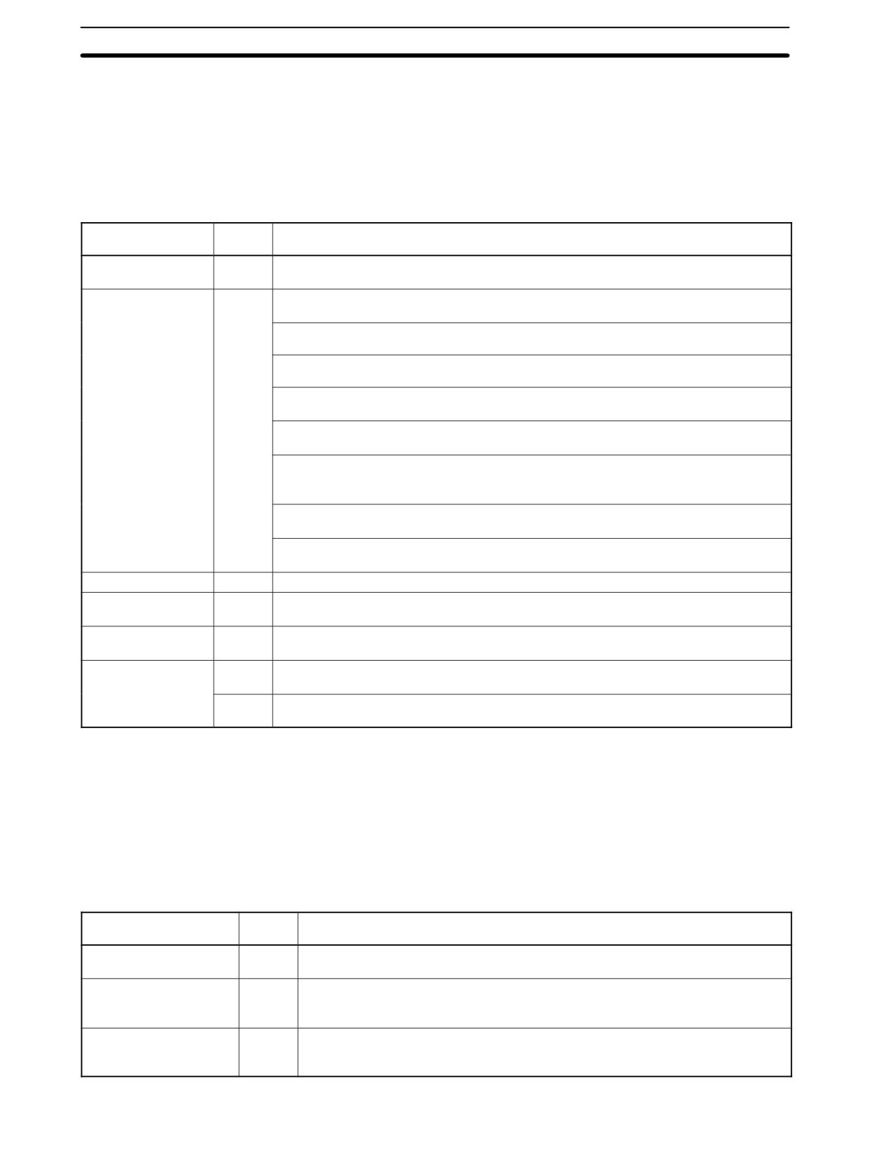
Operating Errors
Section
9-5
9-5-2
Fatal Errors
PC operation and program execution will stop and all outputs from the PC will be
turned OFF when any of these errors have occurred.
All CPU Unit indicators will be OFF for the power interruption error. For all other
fatal operating errors, the POWER and ERR/ALM indicators will be lit. The RUN
indicator will be OFF.
Message
FALS
Meaning and appropriate response
No.
Power interruption
00
Power has been interrupted for at least 10 ms. Check power supply voltage and power
(no message)
lines. Try to power-up again.
MEMORY ERR
F1
AR 1308 ON: An unspecified bit area exists in the user program. Check the program
and correct errors.
AR 1309 ON: An error has occurred in the flash memory. Since the number of writings
to the flash memory has exceeded the specified level, replace the CPU Unit.
AR 1310 ON: A checksum error has occurred in read-only DM (DM 6144 to DM 6599).
Check and correct the settings in the read-only DM area.
AR 1311 ON: A checksum error has occurred in the PC Setup. Initialize all of the PC
Setup and re-input.
AR 1312 ON: A checksum error has occurred in the program. Check the program and
correct any errors detected.
AR 1313 ON: A checksum error has occurred in the expansion instruction’s function
code assignment area. Expansion instruction function codes will be returned to default
settings. Assign function codes again.
AR 1314 ON: Power interruption hold area was not held. Clear the error and reset the
settings of the power interruption hold area.
AR 1315 ON: An error has occurred in CompoBus/S communications. If the error
cannot be corrected, replace the CPU Unit (SRM1(-V2) only).
NO END INST
F0
END(01) is not written in the program. Write END(01) at the end of the program.
I/O BUS ERR
C0
An error has occurred during data transfer between the CPU Unit and an Expansion
(See note 1.)
Unit or Expansion I/O Unit. Check the Unit’s connecting cable.
I/O UNIT OVER
E1
Too many Expansion Units or Expansion I/O Units have been connected. Check the
(See note 1.)
PC configuration.
SYS FAIL FALS**
01 to 99
A FALS(07) instruction has been executed in the program. Check the FALS number to
(See note 2.)
determine the conditions that caused execution, correct the cause, and clear the error.
9F
The cycle time has exceeded the FALS 9F Cycle Time Monitoring Time (DM 6618).
Check the cycle time and adjust the Cycle Time Monitoring Time if necessary.
Note
1. CPM1/CPM1A/CPM2A/CPM2C only.
2. ** is 01 to 99 or 9F.
9-5-3
Other Errors
The PWR indicator will be ON for the following fatal errors. Ignore the status of
other indicators unless a specific status is given in the following table.
Error status
FALS
Meaning and appropriate response
No.
CompoBus/S
None
The ERC indicator will light to indicate an error in CompoBus/S communications.
communications error
Check the slaves and the transmission path and restart the system.
RS-232C port
None
If an error occurs in communications through the RS-232C port, the COMM
communications error
indicator will be OFF and the error flag (AR 0804) will be ON. Check the
connecting cables and restart.
Peripheral port
None
If an error occurs in communications through the peripheral port, the COMM
communications error
indicator will be OFF and the error flag (AR 0812) will be ON. Check the
connecting cables and restart.
550
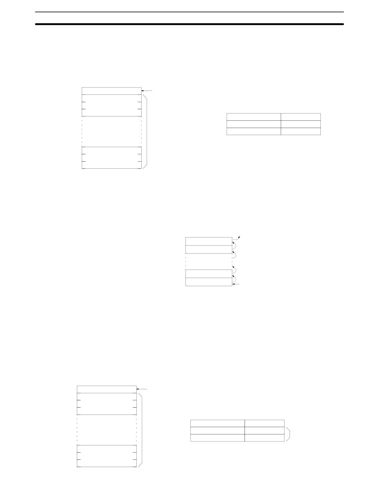
Error Log
Section
9-6
9-6
Error Log
The error log function registers the error code of any fatal or non-fatal error that
occurs in the PC. The date and time at which the error occurred are registered
along with the error code. Refer to page 549 for error codes.
CPM1/CPM1A Error Log
In CPM1/CPM1A PCs, the error log is stored in DM 1000 through DM 1021.
Area
DM1000
Error log pointer
The location for storing the next error record is shown. (0 to 6)
DM1001
Error log record 0
Each error log record is configured as follows:
DM1002
Bit 15
8
7
0
DM1003
Leading word
Error classification
Error code
Leading word + 1
00
00
to
Leading word + 2
00
00
Error classification:
00: Nonfatal
80: Fatal
DM1019
Error log record 9
DM1020
DM1021
Error Log Storage Methods
The error log storage method is set in the PC Setup (DM 6655). Set any of the
following methods.
1, 2, 3...
1. You can store the most recent 10 error log records and discard older re-
cords. This is achieved by shifting the records as shown below so that the
oldest record (record 0) is lost whenever a new record is generated.
Lost
Error log record 1
Error log record 2
All records shifted
Error log record 6
Error log record 7
New record added
2. You can store only the first 10 error log records, and ignore any subsequent
errors beyond those 10.
3. You can disable the log so that no records are stored.
The default setting is the first method. Refer to Error Log Settings on page 21 for
details on the PC Setup for the error log.
Clearing the Error Log
To clear the entire error log, turn ON SR 25214 from a Programming Device. (Af-
ter the error log has been cleared, SR 25214 will turn OFF again automatically.)
CPM2A/CPM2C Error Log
In CPM2A/CPM2C PCs, the error log is stored in DM 2000 through DM 2021. Up
Area
to 7 error records can be stored.
DM 2000
Error log pointer
Indicates the number of records stored in the log (0 to 7). A 0 indi-
cates no records.
DM 2021
Error log record 1
DM 2022
(3 words used.)
Each error log record is configured as follows:
DM 2023
15
8
7
0
Leading word
Error classification
Error code
to
Leading word + 1
Min
Sec
Each stored in
Leading word + 2
Day
Hour
2 digits BCD.
DM 2019
Error classification: 00: Non-fatal
Error log record 7
80: Fatal
DM 2020
(3 words used.)
DM 2021
551
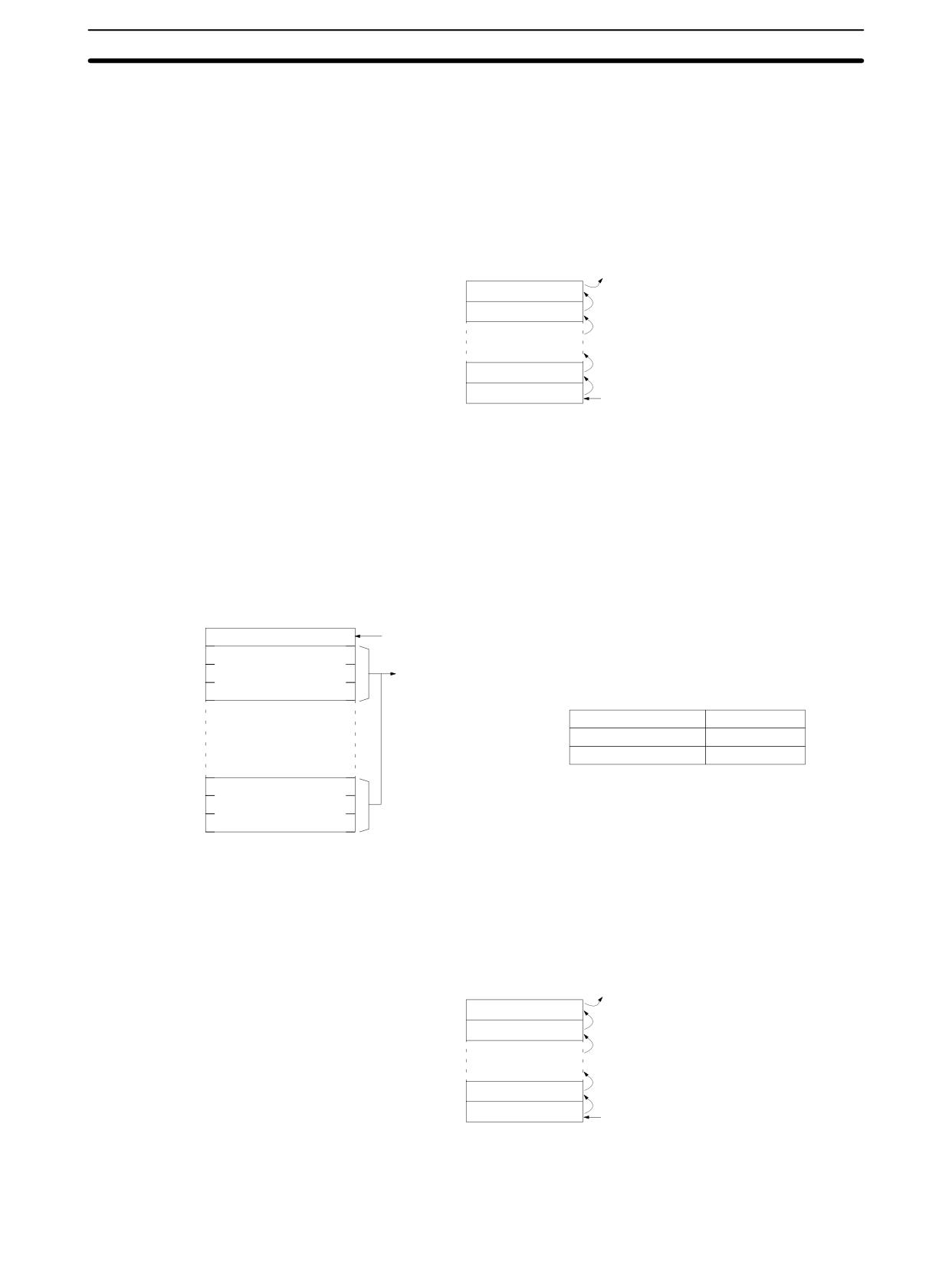
Error Log
Section
9-6
Note An error record with an error code of 00 will be stored in the error log for power
interruptions.
Error Log Storage Methods
The error log storage method is set in the PC Setup (DM 6655). Set any of the
following methods.
1, 2, 3...
1. You can store the most recent 7 error log records and discard older records.
This is achieved by shifting the records as shown below so that the oldest
record (record 0) is lost whenever a new record is generated.
Lost
Error log record 1
Error log record 2
All records shifted
Error log record 6
Error log record 7
New record added
2. You can store only the first 7 error log records, and ignore any subsequent
errors beyond those 7.
3. You can disable the log so that no records are stored.
The default setting is the first method. Refer to Error Log Settings on page 21 for
details on the PC Setup for the error log.
Clearing the Error Log
To clear the entire error log, turn ON SR 25214 from a Programming Device. (Af-
ter the error log has been cleared, SR 25214 will turn OFF again automatically.)
In SRM1(-V2) PCs, the error log is stored in DM 2000 through DM 2021.
SRM1 Error Log Area
DM2000
Error log pointer
Indicates the number of records stored in the log (0 to 7). A 0 indi-
cates no records.
DM2001
Error log record 1
DM2002
Each error log record is configured as follows:
DM2003
Bit 15
8
7
0
Leading word
Error classification
Error code
to
Leading word + 1
00
00
Leading word + 2
00
00
Error classification: 00: Nonfatal
DM2019
Error log record 7
80: Fatal
DM2020
DM2021
Error Log Storage Methods
The error log storage method is set in the PC Setup (DM 6655). Set any of the
following methods.
1, 2, 3...
1. You can store the most recent 7 error log records and discard older records.
This is achieved by shifting the records as shown below so that the oldest
record (record 0) is lost whenever a new record is generated.
Lost
Error log record 1
Error log record 2
All records shifted
Error log record 6
Error log record 7
New record added
2. You can store only the first 7 error log records, and ignore any subsequent
errors beyond those 7.
552
Troubleshooting Flowcharts
Section
9-8
3. You can disable the log so that no records are stored.
The default setting is the first method. Refer to Error Log Settings on page 21 for
details on the PC Setup for the error log.
Clearing the Error Log
To clear the entire error log, turn ON SR 25214 from a Programming Device. (Af-
ter the error log has been cleared, SR 25214 will turn OFF again automatically.)
9-7
Host Link Errors
See 4-3 Host Link Communications for a description of the response format and
the response codes that are returned when a command from a host computer
cannot be processed.
9-8
Troubleshooting Flowcharts
The troubleshooting flowcharts are available in the Operation Manuals.
CPM1 Flowcharts
Refer to 5-6 Troubleshooting Flowcharts in the CPM1 Operation Manual.
CPM1A Flowcharts
Refer to 5-6 Troubleshooting Flowcharts in the CPM1A Operation Manual.
CPM2A Flowcharts
Refer to 5-5 Troubleshooting Flowcharts in the CPM2A Operation Manual.
CPM2C Flowcharts
Refer to 5-5 Troubleshooting Flowcharts in the CPM2C Operation Manual.
SRM1 Flowcharts
Refer to 5-6 Troubleshooting Flowcharts in the SRM1 Operation Manual.
553
Appendix A
Programming Instructions
A PC instruction is input either by pressing the corresponding Programming Console key(s) (e.g., LD, AND, OR,
NOT) or by using function codes. To input an instruction with its function code, press FUN, the function code, and
then WRITE. Refer to the pages listed programming and instruction details.
Code
Mnemonic
Name
Function
Page
—
AND
AND
Logically ANDs status of designated bit with execution condi-
372
tion.
-
AND LD
AND LOAD
Logically ANDs results of preceding blocks.
373
—
AND NOT
AND NOT
Logically ANDs inverse of designated bit with execution
372
condition.
-
CNT
COUNTER
A decrementing counter.
390
—
LD
LOAD
Used to start instruction line with the status of the designated
372
bit or to define a logic block for use with AND LD and OR LD.
-
LD NOT
LOAD NOT
Used to start instruction line with inverse of designated bit.
372
—
OR
OR
Logically ORs status of designated bit with execution condi-
372
tion.
-
OR LD
OR LOAD
Logically ORs results of preceding blocks.
373
—
OR NOT
OR NOT
Logically ORs inverse of designated bit with execution condi-
372
tion.
-
OUT
OUTPUT
Turns ON operand bit for ON execution condition; turns OFF
373
operand bit for OFF execution condition.
-
OUT NOT
OUTPUT NOT
Turns operand bit OFF for ON execution condition; turns op-
373
erand bit ON for OFF execution condition (i.e., inverts opera-
tion).
-
RSET
RESET
Turns the operand bit OFF when the execution condition is
374
ON, and does not affect the status of the operand bit when
the execution condition is OFF.
-
SET
SET
Turns the operand bit ON when the execution condition is
374
ON, and does not affect the status of the operand bit when
the execution condition is OFF.
-
TIM
TIMER
ON-delay (decrementing) timer operation.
385
00
NOP
NO OPERATION
Nothing is executed and program moves to next instruction.
377
01
END
END
Required at the end of the program.
377
02
IL
INTERLOCK
If interlock condition is OFF, all outputs are turned OFF and
377
all timer PVs reset between this IL(02) and the next ILC(03).
Other instructions are treated as NOP; counter PVs are
03
ILC
INTERLOCK CLEAR
377
maintained.
04
JMP
JUMP
If jump condition is OFF, all instructions between JMP(04)
379
and the correspondi
ng JME(05) are
ignored
05
JME
JUMP END
379
06
(@)FAL
FAILURE ALARM AND
Generates a non-fatal error and outputs the designated FAL
381
RESET
number to the Programming Console.
07
FALS
SEVERE FAILURE
Generates a fatal error and outputs the designated FALS
381
ALARM
number to the Programming Console.
08
STEP
STEP DEFINE
When used with a control bit, defines the start of a new step
381
and resets the previous step. When used without N, defines
the end of step execution.
09
SNXT
STEP START
Used with a control bit to indicate the end of the step, reset
381
the step, and start the next step.
10
SFT
SHIFT REGISTER
Creates a bit shift register.
400
11
KEEP
KEEP
Defines a bit as a latch controlled by set and reset inputs.
375
12
CNTR
REVERSIBLE
Increases or decreases PV by one whenever the increment
391
COUNTER
input or decrement input signals, respectively, go from OFF
to ON.
13
DIFU
DIFFERENTIATE UP
Turns ON the designated bit for one cycle on the rising edge
376
of the input signal.
555
Programming Instructions
Appendix A
Code
Mnemonic
Name
Function
Page
14
DIFD
DIFFERENTIATE
Turns ON the bit for one cycle on the trailing edge.
376
DOWN
15
TIMH
HIGH-SPEED TIMER
A high-speed, ON-delay (decrementing) timer.
386
16
(@)WSFT
WORD SHIFT
Shifts data between starting and ending words in word units,
401
writing zeros into starting word.
17 to 19
For expansion instructions.
156
20
CMP
COMPARE
Compares the contents of two words and outputs result to
428
GR, EQ, and LE Flags.
21
(@)MOV
MOVE
Copies source data (word or constant) to destination word.
407
22
(@)MVN
MOVE NOT
Inverts source data (word or constant) and then copies it to
408
destination word.
23
(@)BIN
BCD TO BINARY
Converts four-digit, BCD data in source word into 16-bit
435
binary data, and outputs converted data to result word.
24
(@)BCD
BINARY TO BCD
Converts binary data in source word into BCD, and outputs
436
converted data to result word.
25
(@)ASL
ARITHMETIC SHIFT
Shifts each bit in single word of data one bit to left, with CY.
401
LEFT
26
(@)ASR
ARITHMETIC SHIFT
Shifts each bit in single word of data one bit to right, with CY.
402
RIGHT
27
(@)ROL
ROTATE LEFT
Rotates bits in single word of data one bit to left, with CY.
402
28
(@)ROR
ROTATE RIGHT
Rotates bits in single word of data one bit to right, with CY.
403
29
(@)COM
COMPLEMENT
Inverts bit status of one word of data.
475
30
(@)ADD
BCD ADD
Adds two four-digit BCD values and content of CY, and out-
453
puts result to specified result word.
31
(@)SUB
BCD SUBTRACT
Subtracts a four-digit BCD value and CY from another four-
454
digit BCD value and outputs result to the result word.
32
(@)MUL
BCD MULTIPLY
Multiplies two four-digit BCD values and outputs result to
456
specified result words.
33
(@)DIV
BCD DIVIDE
Divides four-digit BCD dividend by four-digit BCD divisor and
457
outputs result to specified result words.
34
(@)ANDW
LOGICAL AND
Logically ANDs two 16-bit input words and sets correspond-
476
ing bit in result word if corresponding bits in input words are
both ON.
35
(@)ORW
LOGICAL OR
Logically ORs two 16-bit input words and sets corresponding
477
bit in result word if one or both of corresponding bits in input
data are ON.
36
(@)XORW
EXCLUSIVE OR
Exclusively ORs two 16-bit input words and sets bit in result
477
word when corresponding bits in input words differ in status.
37
(@)XNRW
EXCLUSIVE NOR
Exclusively NORs two 16-bit input words and sets bit in result
478
word when corresponding bits in input words are same in
status.
38
(@)INC
BCD INCREMENT
Increments four-digit BCD word by one.
479
39
(@)DEC
BCD DECREMENT
Decrements four-digit BCD word by one.
479
40
(@)STC
SET CARRY
Sets carry flag (i.e., turns CY ON).
453
41
(@)CLC
CLEAR CARRY
Clears carry flag (i.e., turns CY OFF).
453
46
(@)MSG
MESSAGE
Displays a 16-character message on the Programming Con-
493
sole display.
47 & 48
For expansion instructions.
156
50
(@)ADB
BINARY ADD
Adds two four-digit hexadecimal values and content of CY,
463
and outputs result to specified result word.
51
(@)SBB
BINARY SUBTRACT
Subtracts a four-digit hexadecimal value and CY from anoth-
464
er four-digit hexadecimal value and outputs result to the re-
sult word.
52
(@)MLB
BINARY MULTIPLY
Multiplies two four-digit hexadecimal values and outputs re-
466
sult to specified result words.
53
(@)DVB
BINARY DIVIDE
Divides four-digit hexadecimal dividend by four-digit hexade-
466
cimal divisor and outputs result to specified result words.
556
Programming Instructions
Appendix A
Code
Mnemonic
Name
Function
Page
54
(@)ADDL
DOUBLE BCD ADD
Adds two eight-digit values (2 words each) and content of CY,
459
and outputs result to specified result words.
55
(@)SUBL
DOUBLE BCD
Subtracts an eight-digit BCD value and CY from another
460
SUBTRACT
eight-digit BCD value and outputs result to the result words.
56
(@)MULL
DOUBLE BCD
Multiplies two eight-digit BCD values and outputs result to
462
MULTIPLY
specified result words.
57
(@)DIVL
DOUBLE BCD DIVIDE
Divides eight-digit BCD dividend by eight-digit BCD divisor
462
and outputs result to specified result words.
58
(@)BINL
DOUBLE BCD TO
Converts BCD value in two consecutive source words into
436
DOUBLE BINARY
binary and outputs converted data to two consecutive result
words. (CPM2A only)
59
(@)BCDL
DOUBLE BINARY TO
Converts binary value in two consecutive source words into
437
DOUBLE BCD
BCD and outputs converted data to two consecutive result
words. (CPM2A only)
60 to 69
For expansion instructions.
156
70
(@)XFER
BLOCK TRANSFER
Moves content of several consecutive source words to con-
409
secutive destination words.
71
(@)BSET
BLOCK SET
Copies content of one word or constant to several consecu-
410
tive words.
73
(@)XCHG
DATA EXCHANGE
Exchanges contents of two different words.
411
74
(@)SLD
ONE DIGIT SHIFT
Left shifts data between starting and ending words by one
404
LEFT
digit (four bits).
75
(@)SRD
ONE DIGIT SHIFT
Right shifts data between starting and ending words by one
404
RIGHT
digit (four bits).
76
(@)MLPX
4-TO-16 DECODER
Converts up to four hexadecimal digits in source word into
438
decimal values from 0 to 15 and turns ON, in result word(s),
bit(s) whose position corresponds to converted value.
77
(@)DMPX
16-TO-4 ENCODER
Determines position of highest ON bit in source word(s) and
440
turns ON corresponding bit(s) in result word.
78
(@)SDEC
7-SEGMENT
Converts hexadecimal values from source word to data for
442
DECODER
seven-segment display.
80
(@)DIST
SINGLE WORD
Moves one word of source data to destination word whose
411
DISTRIBUTE
address is given by destination base word plus offset.
81
(@)COLL
DATA COLLECT
Extracts data from source word and writes it to destination
413
word.
82
(@)MOVB
MOVE BIT
Transfers designated bit of source word or constant to desig-
415
nated bit of destination word.
83
(@)MOVD
MOVE DIGIT
Moves hexadecimal content of specified four-bit source dig-
416
it(s) to specified destination digit(s) for up to four digits.
84
(@)SFTR
REVERSIBLE SHIFT
Shifts data in specified word or series of words to either left
405
REGISTER
or right.
85
(@)TCMP
TABLE COMPARE
Compares four-digit hexadecimal value with values in table
429
consisting of 16 words.
86
(@)ASC
ASCII CONVERT
Converts hexadecimal values from the source word to eight-
445
bit ASCII code starting at leftmost or rightmost half of starting
destination word.
87 to 89
For expansion instructions.
156
91
(@)SBS
SUBROUTINE ENTRY
Calls and executes subroutine N.
480
92
SBN
SUBROUTINE
Marks start of subroutine N.
482
DEFINE
93
RET
RETURN
Marks the end of a subroutine and returns control to main
482
program.
97
(@)IORF
I/O REFRESH
Refreshes all I/O words between the start and end words.
494
Cannot be used with the SRM1(-V2).
99
(@)MCRO
MACRO
Calls and executes a subroutine replacing I/O words.
482
557
Programming Instructions
Appendix A
Expansion Instructions
The following table shows the instructions that can be treated as expansion instructions in the CPM2A, CPM2C,
and SRM1(-V2) PCs. The default function codes are given for instructions that have codes assigned by default.
Code
Mnemonic
Name
Function
CPU Units
Page
17
(@)ASFT
ASYNCHRONOUS SHIFT
Creates a shift register that exchanges the con-
All
406
REGISTER
tents of adjacent words when one of the words
is zero and the other is not.
47
(@)RXD
RECEIVE
Receives data via a communications port.
All
501
48
(@)TXD
TRANSMIT
Sends data via a communications port.
All
503
60
CMPL
DOUBLE COMPARE
Compares two eight-digit hexadecimal values.
All
432
61
(@)INI
MODE CONTROL
Starts and stops counter operation, compares
All
395
and changes counter PVs, and stops pulse out-
put.
62
(@)PRV
HIGH-SPEED COUNTER
Reads counter PVs and status data for the high-
CPM2A/
397
PV READ
speed counter.
CPM2C
63
(@)CTBL
COMPARISON TABLE
Compares counter PVs and generates a direct
CPM2A/
392
LOAD
table or starts operation.
CPM2C
64
(@)SPED
SPEED OUTPUT
Outputs pulses at the specified frequency (10
CPM2A/
485
Hz to 50 KHz in 10 Hz units). The output fre-
CPM2C
quency can be changed while pulses are being
output.
65
(@)PULS
SET PULSES
Outputs the specified number of pulses at the
CPM2A/
483
specified frequency. The pulse output cannot be
CPM2C
stopped until the specified number of pulses
have been output.
66
(@)SCL
SCALING
Performs a scaling conversion on the calculated
All
417
value.
(But, Ver-
Use the Programming Console or SSS to ac-
sion 2 only
cess this instruction for the SRM1(-V2).
for SRM1)
67
(@)BCNT
BIT COUNTER
Counts the total number of bits that are ON in
All
495
the specified block of words.
68
(@)BCMP
BLOCK COMPARE
Judges whether the value of a word is within 16
All
430
ranges (defined by lower and upper limits).
69
(@)STIM
INTERVAL TIMER
Controls interval timers used to perform sched-
All
500
uled interrupts.
89
(@)INT
INTERRUPT CONTROL
Performs interrupt control, such as masking and
CPM2A/
497
unmasking the interrupt bits for I/O interrupts.
CPM2C
---
(@)ACC
ACCELERATION
Together with PULS(--), ACC(--) controls the
CPM2A/
487
CONTROL
acceleration and/or deceleration of pulses output
CPM2C
from port 1 or 2.
---
AVG
AVERAGE VALUE
Adds the specified number of hexadecimal
CPM2A/
472
words and computes the mean value. Rounds
CPM2C
off to 4 digits past the decimal point.
---
(@)FCS
FCS CALCULATE
Checks for errors in data transmitted by a Host
All
496
Link command.
---
(@)HEX
ASCII-TO-HEXADECIMAL
Converts ASCII data to hexadecimal data.
All
447
---
(@)HMS
SECONDS TO HOURS
Converts second data to hour and minute data.
CPM2A/
450
CPM2C
---
(@)MAX
FIND MAXIMUM
Finds the maximum value in specified data area
CPM2A/
468
and outputs that value to another word.
CPM2C
---
(@)MIN
FIND MINIMUM
Finds the minimum value in specified data area
CPM2A/
470
and outputs that value to another word.
CPM2C
---
(@)NEG
2’S COMPLEMENT
Converts the four-digit hexadecimal content of
All
451
the source word to its 2’s complement and out-
(But, Ver-
puts the result to R.
sion 2 only
Use the Programming Console or SSS to ac-
for SRM1)
cess this instruction for the SRM1(-V2).
558

Programming Instructions
Appendix A
Code
Mnemonic
Name
Function
CPU Units
Page
---
PID
PID CONTROL
Performs PID control based on the specified
All
422
parameters.
(But, Ver-
Use the Programming Console or SSS to ac-
sion 2 only
cess this instruction for the SRM1(-V2).
for SRM1)
---
(@)PWM
PULSE WITH VARIABLE
Outputs pulses with the specified duty ratio (0%
CPM2A/
490
DUTY RATIO
to 99%) from port 1 or 2.
CPM2C
---
(@)SCL2
SIGNED BINARY TO BCD
Linearly converts a 4-digit signed hexadecimal
CPM2A/
418
SCALING
value to a 4-digit BCD value.
CPM2C
---
(@)SCL3
BCD TO SIGNED BINARY
Linearly converts a 4-digit BCD value to a 4-digit
CPM2A/
420
SCALING
signed hexadecimal value.
CPM2C
---
(@)SEC
HOURS TO SECONDS
Converts hour and minute data to second data.
CPM2A/
449
CPM2C
---
(@)SRCH
DATA SEARCH
Searches the specified range of memory for the
CPM2A/
467
specified data. Outputs the word address(es) of
CPM2C
words in the range that contain the data.
---
(@)STUP
CHANGE RS-232C
Changes the communications parameters in the
All
505
SETUP
PC Setup for a specified port.
---
(@)SUM
SUM CALCULATE
Computes the sum of the contents of the words
CPM2A/
474
in the specified range of memory.
CPM2C
---
SYNC
SYNCHRONIZED PULSE
Multiplies an input pulse frequency by a fixed
CPM2A/
492
CONTROL
scaling factor and outputs pulses from the speci-
CPM2C
fied output bit at the resulting frequency.
---
TIML
LONG TIMER
A decrementing ON-delay timer with SV of up to
CPM2A/
388
99,990 s
CPM2C
---
TMHH
VERY HIGH-SPEED
A high-speed, decrementing ON-delay timer that
CPM2A/
387
TIMER
times in 1-ms units
CPM2C
---
ZCP
AREA RANGE COMPARE
Compares a word to a range defined by lower
All
433
and upper limits and outputs the result to the
(But, Ver-
GR, EQ, and LE flags.
sion 2 only
Use the Programming Console or SSS to ac-
for SRM1)
cess this instruction for the SRM1(-V2).
---
ZCPL
DOUBLE AREA RANGE
Compares an 8-digit value to a range defined by
CPM2A/
434
COMPARE
lower and upper limits and outputs the result to
CPM2C
the GR, EQ, and LE flags.
559
Appendix B
Error and Arithmetic Flag Operation
The following table shows the instructions that affect the ER, CY, GT, LT and EQ flags. In general, ER indicates that
operand data is not within requirements. CY indicates arithmetic or data shift results. GT indicates that a compared
value is larger than some standard, LT that it is smaller, and EQ, that it is the same. EQ also indicates a result of
zero for arithmetic operations. Refer to Section 7 Instruction Set for details.
Vertical arrows in the table indicate the flags that are turned ON and OFF according to the result of the instruction.
Although ladder diagram instructions,TIM, and CNT are executed when ER is ON, other instructions with a vertical
arrow under the ER column are not executed if ER is ON. All of the other flags in the following table will also not
operate when ER is ON.
Instructions not shown do not affect any of the flags in the table. Although only the non-differentiated form of each
instruction is shown, differentiated instructions affect flags in exactly the same way.
The ER, CY, GT, LT and EQ Flags are turned OFF when END(01) is executed, so their status cannot be monitored
with a Programming Device.
The status of the ER, CY, GT, LT and EQ Flags is affected by instruction execution and will change each time an
instruction that affects them is executed. Differentiated instructions are executed only once when their execution
condition changes (ON to OFF or OFF to ON) and are not executed again until the next specified change in their
execution condition. The status of the ER, CY, GT, LT and EQ Flags is thus affected by a differentiated instruction
only when the execution condition changes and is not affected during scans when the instruction is not executed,
i.e., when the specified change does not occur in the execution condition. When a differentiated instruction is not
executed, the status of the ER, CY, GT, LT and EQ Flags will not change and will maintain the status produced by
the last instruction that was executed.
Instructions
25503 (ER)
25504 (CY)
25505 (GR)
25506 (EQ)
25507 (LE)
25402 (N)
Page
TIM
Unaffected
Unaffected
Unaffected
Unaffected
Unaffected
385
CNT
390
END(01)
OFF
OFF
OFF
OFF
OFF
OFF
377
STEP(08)
Unaffected
Unaffected
Unaffected
Unaffected
Unaffected
Unaffected
381
SNXT(09)
381
CNTR(12)
391
TIMH(15)
386
WSFT(16)
401
CMP(20)
Unaffected
Unaffected
428
MOV(21)
Unaffected
Unaffected
Unaffected
407
MVN(22)
408
BIN(23)
OFF
435
BCD(24)
Unaffected
436
ASL(25)
Unaffected
Unaffected
401
ASR(26)
OFF
402
ROL(27)
402
ROR(28)
403
COM(29)
Unaffected
Unaffected
Unaffected
475
ADD(30)
Unaffected
453
SUB(31)
454
561
Error and Arithmetic Flag Operation
Appendix B
Instructions
25503 (ER)
25504 (CY)
25505 (GR)
25506 (EQ)
25507 (LE)
25402 (N)
Page
MUL(32)
Unaffected
Unaffected
Unaffected
Unaffected
456
DIV(33)
457
ANDW(34)
476
ORW(35)
477
XORW(36)
477
XNRW(37)
478
INC(38)
Unaffected
479
DEC(39)
479
STC(40)
Unaffected
ON
Unaffected
Unaffected
Unaffected
Unaffected
453
CLC(41)
OFF
453
MSG(46)
Unaffected
493
ADB(50)
Unaffected
Unaffected
463
SBB(51)
464
MLB(52)
Unaffected
Unaffected
Unaffected
466
DVB(53)
Unaffected
Unaffected
Unaffected
466
ADDL(54)
Unaffected
459
SUBL(55)
460
MULL(56)
Unaffected
Unaffected
Unaffected
Unaffected
462
DIVL(57)
462
BINL(58)
OFF
436
BCDL(59)
Unaffected
437
XFER(70)
Unaffected
Unaffected
Unaffected
Unaffected
Unaffected
409
BSET(71)
410
XCHG(73)
Unaffected
Unaffected
Unaffected
Unaffected
Unaffected
411
SLD(74)
404
SRD(75)
404
MLPX(76)
438
DMPX(77)
440
SDEC(78)
442
DIST(80)
Unaffected
Unaffected
Unaffected
411
COLL(81)
413
MOVB(82)
Unaffected
Unaffected
415
MOVD(83)
416
SFTR(84)
Unaffected
Unaffected
Unaffected
Unaffected
405
TCMP(85)
Unaffected
429
ASC(86)
Unaffected
445
SBS(91)
480
MCRO(99)
482
562
Error and Arithmetic Flag Operation
Appendix B
Expansion Instructions (CPM2A/CPM2C and SRM1(-V2))
Instructions
25503 (ER)
25504 (CY)
25505 (GR)
25506 (EQ)
25507 (LE)
25402 (N)
Page
ASFT(17)
Unaffected
Unaffected
Tnaffected
Unaffected
Unaffected
406
RXD(47)
501
TXD(48)
503
CMPL(60)
432
INI(61)
Unaffected
Unaffected
Unaffected
Unaffected
395
PRV(62)
397
CTBL(63)
392
SPED(64)
485
PULS(65)
483
SCL(66)
Unaffected
417
BCNT(67)
495
BCMP(68)
Unaffected
430
STIM(69)
500
INT(89)
497
SRCH(--)
467
MAX(--)
468
MIN(--)
470
HMS(--)
Unaffected
450
NEG(--)*
451
SEC(--)
449
SUM(--)
474
FCS(--)
Unaffected
Unaffected
496
HEX(--)
Unaffected
447
AVG(--)
472
PID(--)
422
ZCP(--)
Unaffected
433
Note *Depending on the results, NEG(--) may also affect the status of the underflow flag (SR 25405).
Expansion Instructions (CPM2A/CPM2C Only)
Instructions
25503 (ER)
25504 (CY)
25505 (GR)
25506 (EQ)
25507 (LE)
Page
PWM(--)
Unaffected
Unaffected
Unaffected
Unaffected
490
ZCPL(--)
434
ACC(--)
487
SCL2(--)
Unaffected
Unaffected
418
SCL3(--)
Unaffected
420
SYNC(--)
420
563
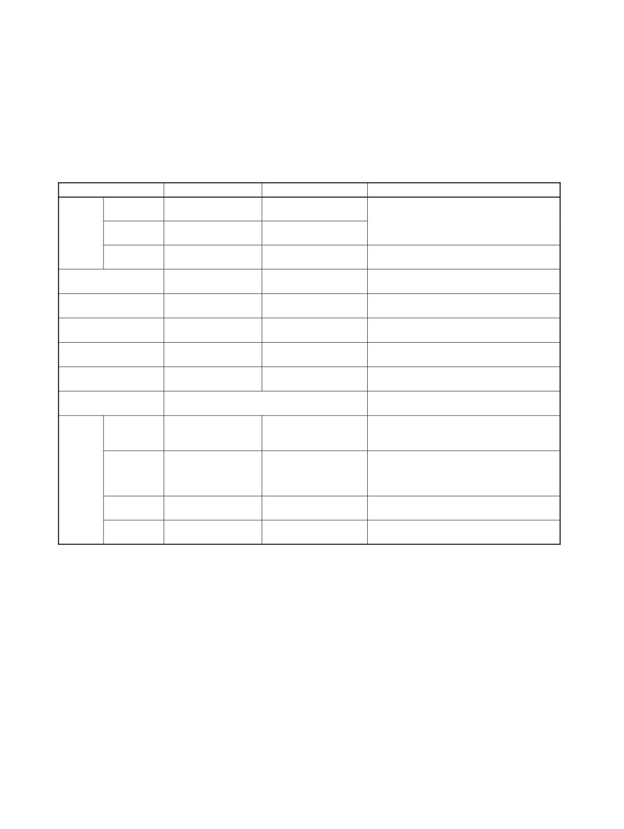
Appendix C
Memory Areas
CPM1/CPM1A Memory Areas
Memory Area Structure
The following memory areas can be used with the CPM1/CPM1A.
Data area
Words
Bits
Function
IR area1
Input area
IR 000 to IR 009
IR 00000 to IR 00915
These bits can be allocated to the external
(10 words)
(160 bits)
I/O terminals.
Output area
IR 010 to IR 019
IR 01000 to IR 01915
(10 words)
(160 bits)
Work area
IR 200 to IR 231
IR 20000 to IR 23115
Work bits can be freely used within the pro-
(32 words)
(512 bits)
gram.
SR area
SR 232 to SR 255
SR 23200 to SR 25515
These bits serve specific functions such as
(24 words)
(384 bits)
flags and control bits.
TR area
---
TR 0 to TR 7
These bits are used to temporarily store
(8 bits)
ON/OFF status at program branches.
HR area2
HR 00 to HR 19
HR 0000 to HR 1915
These bits store data and retain their ON/
(20 words)
(320 bits)
OFF status when power is turned off.
AR area2
AR 00 to AR 15
AR 0000 to AR 1515
These bits serve specific functions such as
(16 words)
(256 bits)
flags and control bits.
LR area1
LR 00 to LR 15
LR 0000 to LR 1515
Used for a 1:1 data link with another PC.
(16 words)
(256 bits)
Timer/Counter area2
TC 000 to TC 127 (timer/counter numbers)3
The same numbers are used for both timers
and counters.
DM area
Read/write2
DM 0000 to DM 0999
---
DM area data can be accessed in word
DM 1022 to DM 1023
units only. Word values are retained when
(1,002 words)
the power is turned off.
Error log2
DM 1000 to DM 1021
---
Used to store the error code of errors that
(22 words)
occur. These words can be used as ordi-
nary read/write DM when the error log func-
tion isn’t being used.
Read-only4
DM 6144 to DM 6599
---
Cannot be overwritten from program.
(456 words)
PC Setup4
DM 6600 to DM 6655
---
Used to store various parameters that con-
(56 words)
trol PC operation.
Note 1. IR and LR bits that are not used for their allocated functions can be used as work bits.
2. The contents of the HR area, AR area, Counter area, and read/write DM area are backed up by a capaci-
tor. The backup time varies with the ambient temperature, but at 25_C, the capacitor will back up
memory for 20 days. If the power supply is off longer than the backup time, memory contents will be
cleared and AR1314 will turn ON. (This flag turns ON when data can no longer be retained by the built-in
capacitor.) Refer to 2-1-2 Characteristics in the CPM1 Operation Manual for a graph showing the back-
up time vs. temperature.
3. When accessing a PV, TC numbers are used as word data; when accessing Completion Flags, they are
used as bit data.
4. Data in DM 6144 to DM 6655 cannot be overwritten from the program, but they can be changed from a
Programming Device.
SR Area
These bits mainly serve as flags related to CPM1/CPM1A operation or contain present and set values for various
functions. The functions of the SR area are explained in the following table.
Note “Read-only” words and bits can be read as status in controller PC operation, but they cannot be written from
the ladder program. Bits and words that are “Not used” are also read-only.
565
Memory Areas
Appendix C
Word(s)
Bit(s)
Function
Read/
Page
write
SR 232
00 to 15
Macro Function Input Area
Read/
153
to
Contains the input operands for MCRO(99).
write
SR 235
(Can be used as work bits when MCRO(99) is not used.)
SR 236
00 to 15
Macro Function Output Area
to
Contains the output operands for MCRO(99).
SR 239
(Can be used as work bits when MCRO(99) is not used.)
SR 240
00 to 15
Input Interrupt 0 Counter Mode SV
77
SV when input interrupt 0 is used in counter mode (4 digits hexadecimal).
(Can be used as work bits when input interrupt 0 is not used in counter
mode.)
SR 241
00 to 15
Input Interrupt 1 Counter Mode SV
SV when input interrupt 1 is used in counter mode (4 digits hexadecimal).
(Can be used as work bits when input interrupt 1 is not used in counter
mode.)
SR 242
00 to 15
Input Interrupt 2 Counter Mode SV
SV when input interrupt 2 is used in counter mode (4 digits hexadecimal).
(Can be used as work bits when input interrupt 2 is not used in counter
mode.)
SR 243
00 to 15
Input Interrupt 3 Counter Mode SV
SV when input interrupt 3 is used in counter mode (4 digits hexadecimal).
(Can be used as work bits when input interrupt 3 is not used in counter
mode.)
SR 244
00 to 15
Input Interrupt 0 Counter Mode PV Minus One
Read-
78
Counter PV-1 when input interrupt 0 is used in counter mode (4 digits hexa-
only
decimal).
SR 245
00 to 15
Input Interrupt 1 Counter Mode PV Minus One
Counter PV-1 when input interrupt 1 is used in counter mode (4 digits hexa-
decimal).
SR 246
00 to 15
Input Interrupt 2 Counter Mode PV Minus One
Counter PV-1 when input interrupt 2 is used in counter mode (4 digits hexa-
decimal).
SR 247
00 to 15
Input Interrupt 3 Counter Mode PV Minus One
Counter PV-1 when input interrupt 3 is used in counter mode (4 digits hexa-
decimal).
SR 248,
00 to 15
High-speed Counter PV Area
83
SR 249
(Can be used as work bits when the high-speed counter is not used.)
SR 250
00 to 15
Analog Setting 0
146
Used to store the 4-digit BCD set value (0000 to 0200) from analog control 0.
SR 251
00 to 15
Analog Setting 1
Used to store the 4-digit BCD set value (0000 to 0200) from analog control 1.
566
Memory Areas
Appendix C
Word(s)
Bit(s)
Function
Read/
Page
write
SR 252
00
High-speed Counter Reset Bit
Read/
84
write
01 to 07
Not used.
08
Peripheral Port Reset Bit
Read/
268
Turn ON to reset peripheral port. (Not valid when Programming Device is
write
connected.) Automatically turns OFF when reset is complete.
09
Not used.
10
PC Setup Reset Bit
Read/
2
Turn ON to initialize PC Setup (DM 6600 through DM 6655). Automatically
write
turns OFF again when reset is complete. Only effective if the PC is in PRO-
GRAM mode.
11
Forced Status Hold Bit (See note.)
17
OFF: The forced status of bits that are forced set/reset is cleared when
switching between PROGRAM mode and MONITOR mode.
ON: The status of bits that are forced set/reset are maintained when switch-
ing between PROGRAM mode and MONITOR mode.
The status of this bit can be maintained when PC power turns off by using the
PC Setup.
12
I/O Hold Bit (See note.)
17
OFF: IR and LR bits are reset when starting or stopping operation.
ON: IR and LR bit status is maintained when starting or stopping operation.
The status of this bit can be maintained when PC power turns off by using the
PC Setup.
13
Not used.
14
Error Log Reset Bit
Read/
551
Turn ON to clear error log. Automatically turns OFF again when operation is
write
complete.
15
Not used.
SR 253
00 to 07
FAL Error Code
Read-
381
The error code (a 2-digit number) is stored here when an error occurs. The
only
FAL number is stored here when FAL(06) or FALS(07) is executed. This word
is reset (to 00) by executing a FAL 00 instruction or by clearing the error from
a Programming Device.
08
Not used.
09
Cycle Time Overrun Flag
Read-
---
Turns ON when a cycle time overrun occurs (i.e., when the cycle time ex-
only
ceeds 100 ms).
10 to 12
Not used.
13
Always ON Flag
Read-
---
only
14
Always OFF Flag
---
15
First Cycle Flag
---
Turns ON for 1 cycle at the start of operation.
SR 254
00
1-minute clock pulse (30 seconds ON; 30 seconds OFF)
---
01
0.02-second clock pulse (0.01 second ON; 0.01 second OFF)
---
02
Negative (N) Flag
---
03 to 05
Not used.
06
Differential Monitor Complete Flag
Read-
155
Turns ON when differential monitoring is complete.
only
07
STEP(08) Execution Flag
381
Turns ON for 1 cycle only at the start of process based on STEP(08).
08 to 15
Not used.
567
Memory Areas
Appendix C
Word(s)
Bit(s)
Function
Read/
Page
write
SR 255
00
0.1-second clock pulse (0.05 second ON; 0.05 second OFF)
Read-
---
only
01
0.2-second clock pulse (0.1 second ON; 0.1 second OFF)
---
02
1.0-second clock pulse (0.5 second ON; 0.5 second OFF)
---
03
Instruction Execution Error (ER) Flag
---
Turns ON when an error occurs during execution of an instruction.
04
Carry (CY) Flag
---
Turns ON when there is a carry in the results of an instruction execution.
05
Greater Than (GR) Flag
---
Turns ON when the result of a comparison operation is “greater.”
06
Equals (EQ) Flag
---
Turns ON when the result of a comparison operation is “equal,” or when the
result of an instruction execution is 0.
07
Less Than (LE) Flag
---
Turns ON when the result of a comparison operation is “less.”
08 to 15
Not used.
Note DM 6601 in the PC Setup can be set to maintain the previous status of the I/O Hold Bit (SR 25212) and the
I/O Hold Bit (SR 25212) when power is turned OFF. If power is left OFF for longer than the backup time,
however, status may be cleared. For details regarding the backup time, refer to the CPM1A or CPM1
Operation Manual. Refer to 1-1-2 CPM1/CPM1A PC Setup Settings for details on the PC Setup.
AR Area
These bits mainly serve as flags related to CPM1/CPM1A operation. These bits retain their status even after the
CPM1/CPM1A power supply has been turned off or when operation begins or stops.
Word(s)
Bit(s)
Function
Page
AR 00,
00 to 15
Not used.
AR 01
AR 02
00
Expansion Unit Error Flag for 1st Unit
These flags turn ON
---
when there
is an error
in
01
Expansion Unit Error Flag for 2nd Unit
the corresponding Unit.
(Not used by CPM1 CPU Units without “-V1” suffix.)
02
Expansion Unit Error Flag for 3rd Unit
(Not used by CPM1 CPU Units without “-V1” suffix.)
03 to 07
Not used.
08 to 11
Number of I/O Units Connected
---
12 to 15
Not used.
AR 03 to
00 to 15
Not used.
AR 07
AR 08
00 to 07
Not used.
08 to 11
Programming Device Error Code
269
0: Normal completion
1: Parity error
2: Frame error
3: Overrun error
12
Programming Device Error Flag
13 to 15
Not used.
AR 09
00 to 15
Not used.
AR 10
00 to 15
Power-off Counter (4 digits BCD)
---
This is the count of the number of times that the power has been turned off.
To clear the count, write “0000” from a Programming Device.
568
Memory Areas
Appendix C
Word(s)
Bit(s)
Function
Page
AR 11
00 to 07
High-speed Counter Range Comparison Flags
86
00 ON: Counter PV is within comparison range 1
01 ON: Counter PV is within comparison range 2
02 ON: Counter PV is within comparison range 3
03 ON: Counter PV is within comparison range 4
04 ON: Counter PV is within comparison range 5
05 ON: Counter PV is within comparison range 6
06 ON: Counter PV is within comparison range 7
07 ON: Counter PV is within comparison range 8
08 to 14
Not used.
15
Pulse Output Status
---
ON:
Stopped.
OFF:
Pulses being output.
AR 12
00 to 15
Not used.
AR 13
00
Power-up PC Setup Error Flag
549
Turns ON when there is an error in DM 6600 to DM 6614 (the part of the PC Setup area
that is read at power-up).
01
Start-up PC Setup Error Flag
Turns ON when there is an error in DM 6615 to DM 6644 (the part of the PC Setup area
that is read at the beginning of operation).
02
RUN PC Setup Error Flag
Turns ON when there is an error in DM 6645 to DM 6655 (the part of the PC Setup area
that is always read).
03, 04
Not used.
05
Long Cycle Time Flag
---
Turns ON if the actual cycle time is longer than the cycle time set in DM 6619.
06, 07
Not used.
08
Memory Area Specification Error Flag
---
Turns ON when a non-existent data area address is specified in the program.
09
Flash Memory Error Flag
---
Turns ON when there is an error in flash memory.
10
Read-only DM Error Flag (See note 3.)
550
Turns ON when a checksum error occurs in the read-only DM (DM 6144 to DM 6599)
and that area is initialized.
11
PC Setup Error Flag
Turns ON when a checksum error occurs in the PC Setup area.
12
Program Error Flag
---
Turns ON when a checksum error occurs in the program memory (UM) area, or when
an improper instruction is executed.
13
Not used.
14
Data Save Error Flag
---
Turns ON when power is turned on if data could not be saved with the built-in capacitor.
Data is saved in the following areas with the built-in capacitor:
DM area (Read/write-capable: DM 0000 to 0999 and DM 1022 to 1023)
HR area (HR 00 to 19)
Counter area (CNT 000 to 127)
SR area, word 252, bits 11, 12 (when PC Setup in DM 6601 is set to maintain status)
AR area, word 10 (power-off counter)
Operation mode (when PC Setup in DM 6600 is set to continue mode last used before
power failure)
If data could not be saved in the above areas:
The DM, error log, HR, counter, SR (word 252, bits 11 and 12), and AR (word 10) areas
will be cleared and the operating mode will go into PROGRAM mode if DM 0000 is set
to continue mode last used before power failure or if DM6604 is set to generate an er-
ror.
(For details regarding the holding time, refer to the CPM1A Operation Manual.)
15
Not used.
569

Memory Areas
Appendix C
Word(s)
Bit(s)
Function
Page
AR 14
00 to 15
Maximum Cycle Time (4 digits BCD) (See note 1.)
533
The longest cycle time since the beginning of operation is stored. It is cleared at the
beginning, and not at the end, of operation.
The units can be any of the following, depending on the setting of in DM 6618.
Default: 0.1 ms; “10 ms” setting: 0.1 ms; “100 ms” setting: 1 ms; “1 s” setting: 10 ms
AR 15
00 to 15
Current Cycle Time (4 digits BCD) (See note 1.)
The most recent cycle time during operation is stored. The Current Cycle Time is not
cleared when operation stops.
The units can be any of the following, depending on the setting of in DM 6618.
Default: 0.1 ms; “10 ms” setting: 0.1 ms; “100 ms” setting: 1 ms; “1 s” setting: 10 ms
Note 1. The units will be as follows, depending on the unit setting for the cycle monitor time (DM 6618):
Initial status:
0.1-ms unit
When 10-ms unit is set:
0.1-ms unit
When 100-ms unit is set:
1-ms unit
When 1-s unit is set:
10-ms unit
2. Areas that cannot be used are cleared when the power is turned on.
3. The contents of AR 10 is backed up by the built-in capacitor. If power is left OFF for longer than the back-
up time, however, the contents may be cleared. For details regarding the backup time, refer to the
CPM1A or CPM1 Operation Manual.
CPM2A/CPM2C Memory Areas
Memory Area Structure
The following memory areas can be used with the CPM2A/CPM2C. Refer to the CPM2C-S Operation Manual
(W377) for information on CPM2C-S memory areas.
Data area
Words
Bits
Function
IR area1
Input area
IR 000 to IR 009
IR 00000 to IR 00915
These bits can be allocated to the external
(10 words)
(160 bits)
I/O terminals.
Output area
IR 010 to IR 019
IR 01000 to IR 01915
(10 words)
(160 bits)
Work area
IR 020 to IR 049
IR 02000 to IR 04915
Work bits can be freely used within the pro-
IR 200 to IR 227
IR 20000 to IR 22715
gram.
(58 words)
(928 bits)
SR area
SR 228 to SR 255
SR 22800 to SR 25515
These bits serve specific functions such as
(28 words)
(448 bits)
flags and control bits.
TR area
---
TR 0 to TR 7
These bits are used to temporarily store
(8 bits)
ON/OFF status at program branches.
HR area2
HR 00 to HR 19
HR 0000 to HR 1915
These bits store data and retain their ON/
(20 words)
(320 bits)
OFF status when power is turned off.
AR area2
AR 00 to AR 23
AR 0000 to AR 2315
These bits serve specific functions such as
(24 words)
(384 bits)
flags and control bits.
LR area1
LR 00 to LR 15
LR 0000 to LR 1515
Used for a 1:1 data link with another PC.
(16 words)
(256 bits)
Timer/Counter area2
TC 000 to TC 255 (timer/counter numbers)3
The same numbers are used for both timers
and counters.
DM area
Read/write2
DM 0000 to DM 1999
---
DM area data can be accessed in word
DM 2022 to DM 2047
units only. Word values are retained when
(2,026 words)
the power is turned off.
Error log2
DM 2000 to DM 2021
---
Used to store the error code of errors that
(22 words)
occur. These words can be used as ordi-
nary read/write DM when the error log func-
tion isn’t being used.
Read-only4
DM 6144 to DM 6599
---
Cannot be overwritten from program.
(456 words)
PC Setup4
DM 6600 to DM 6655
---
Used to store various parameters that con-
(56 words)
trol PC operation.
570
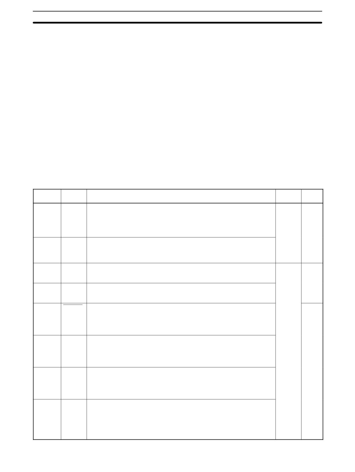
Memory Areas
Appendix C
Note 1. IR and LR words that are not used for their allocated functions can be used as work words.
2. The contents of the HR area, AR area, Counter area, and read/write DM area are backed up by the CPU
Unit’s battery. If the battery is removed or fails, the data in these areas will be lost and reset to default
values. (In CPM2C CPU Units without a battery, these areas are backed up by a capacitor. At 25_C, the
capacitor will back up memory for 10 days.)
3. When a TC number is used as a word operand, it accesses the timer or counter’s PV; when used as a bit
operand, it accesses the Completion Flag.
4. Data in DM 6144 to DM 6655 cannot be overwritten from the program, but they can be changed from a
Programming Device. The program and data in DM 6144 to DM 6655 are backed up in flash memory.
SR Area
These bits mainly serve as flags related to CPM2A/CPM2C operation or contain present and set values for various
functions. The functions of the SR area are explained in the following table.
Note “Read-only” words and bits can be read as status in controller PC operation, but they cannot be written from
the ladder program. Bits and words that are “Not used” are also read-only.
Word(s)
Bit(s)
Function
Read/
Page
write
SR 228,
00 to 15
Pulse Output PV 0
Read-
102
SR 229
Contains the pulse output PV (-16,777,215 to 16,777,215). SR 22915 acts as
only
the sign bit; a negative number is indicated when SR 22915 is ON.
(The same PV data can be read immediately with PRV(62).)
Only Pulse Output PV 0 is used for ACC(--).
SR 230,
00 to 15
Pulse Output PV 1
SR 231
Contains the pulse output PV (-16,777,215 to 16,777,215). SR 23115 acts as
the sign bit; a negative number is indicated when SR 23115 is ON.
(The same PV data can be read immediately with PRV(62).)
SR 232
00 to 15
Macro Function Input Area
Read/
153
to
Contains the input operands for MCRO(99).
write
SR 235
(Can be used as work bits when MCRO(99) is not used.)
SR 236
00 to 15
Macro Function Output Area
to
Contains the output operands for MCRO(99).
SR 239
(Can be used as work bits when MCRO(99) is not used.)
SR 240
00 to 15
Interrupt Input 00003 Counter Mode SV
69
SV when interrupt input 00003 is used in counter mode (4 digits hexadeci-
mal).
(Can be used as work bits when interrupt input 00003 is not used in counter
mode.)
SR 241
00 to 15
Interrupt Input 00004 Counter Mode SV
SV when interrupt input 00004 is used in counter mode (4 digits hexadeci-
mal).
(Can be used as work bits when interrupt input 00004 is not used in counter
mode.)
SR 242
00 to 15
Interrupt Input 00005 Counter Mode SV
SV when interrupt input 00005 is used in counter mode (4 digits hexadeci-
mal).
(Can be used as work bits when interrupt input 00005 is not used in counter
mode.)
SR 243
00 to 15
Interrupt Input 00006 Counter Mode SV
SV when interrupt input 00006 is used in counter mode (4 digits hexadeci-
mal).
(Can be used as work bits when interrupt input 00006 is not used in counter
mode.)
(Input 00006 does not exist in CPM2C CPU Units with 10 I/O points.)
571
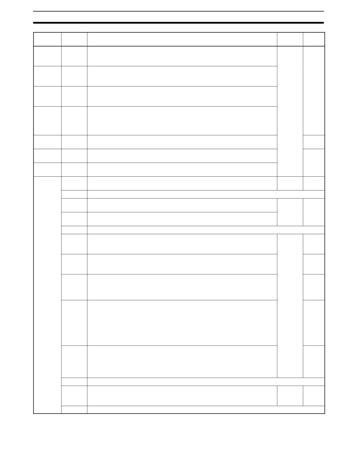
Memory Areas
Appendix C
Word(s)
Bit(s)
Function
Read/
Page
write
SR 244
00 to 15
Interrupt Input 00003 Counter Mode PV
Read-
71
Counter PV when interrupt input 00003 is used in counter mode (4 digits hex-
only
adecimal).
SR 245
00 to 15
Interrupt Input 00004 Counter Mode PV
Counter PV when interrupt input 00004 is used in counter mode (4 digits hex-
adecimal).
SR 246
00 to 15
Interrupt Input 00005 Counter Mode PV
Counter PV when interrupt input 00005 is used in counter mode (4 digits hex-
adecimal).
SR 247
00 to 15
Interrupt Input 00006 Counter Mode PV
Counter PV when interrupt input 00006 is used in counter mode (4 digits hex-
adecimal).
(Input 00006 does not exist in CPM2C CPU Units with 10 I/O points.)
SR 248,
00 to 15
High-speed Counter PV Area
56
SR 249
(Can be used as work bits when the high-speed counter is not used.)
SR 250
00 to 15
Analog Setting 0 (CPM2A PCs only)
146
Used to store the 4-digit BCD set value (0000 to 0200) from analog control 0.
SR 251
00 to 15
Analog Setting 1 (CPM2A PCs only)
Used to store the 4-digit BCD set value (0000 to 0200) from analog control 1.
SR 252
00
High-speed Counter Reset Bit
Read/
48
write
01 to 03
Not used.
04
Pulse Output 0 PV Reset Bit
Read/
93
Turn ON to clear the PV of pulse output 0.
write
05
Pulse Output 1 PV Reset Bit
Turn ON to clear the PV of pulse output 1.
06, 07
Not used.
08
Peripheral Port Reset Bit
Read/
---
Turn ON to reset the peripheral port. Automatically turns OFF when reset is
write
complete.
09
RS-232C Port Reset Bit
---
Turn ON to reset the RS-232C port. Automatically turns OFF when reset is
complete.
10
PC Setup Reset Bit
2
Turn ON to initialize PC Setup (DM 6600 through DM 6655). Automatically
turns OFF again when reset is complete. Only effective if the PC is in PRO-
GRAM mode.
11
Forced Status Hold Bit (See note.)
17
OFF: The forced status of bits that are forced set/reset is cleared when
switching between PROGRAM mode and MONITOR mode.
ON: The status of bits that are forced set/reset are maintained when switch-
ing between PROGRAM mode and MONITOR mode.
The PC Setup can be set to maintain the status of this bit when the PC is
turned off.
12
I/O Hold Bit (See note.)
17
OFF: IR and LR bits are reset when starting or stopping operation.
ON: IR and LR bit status is maintained when starting or stopping operation.
The PC Setup can be set to maintain the status of this bit when the PC is
turned off.
13
Not used.
14
Error Log Reset Bit
Read/
551
Turn ON to clear error log. Automatically turns OFF again when operation is
write
complete.
15
Not used.
572
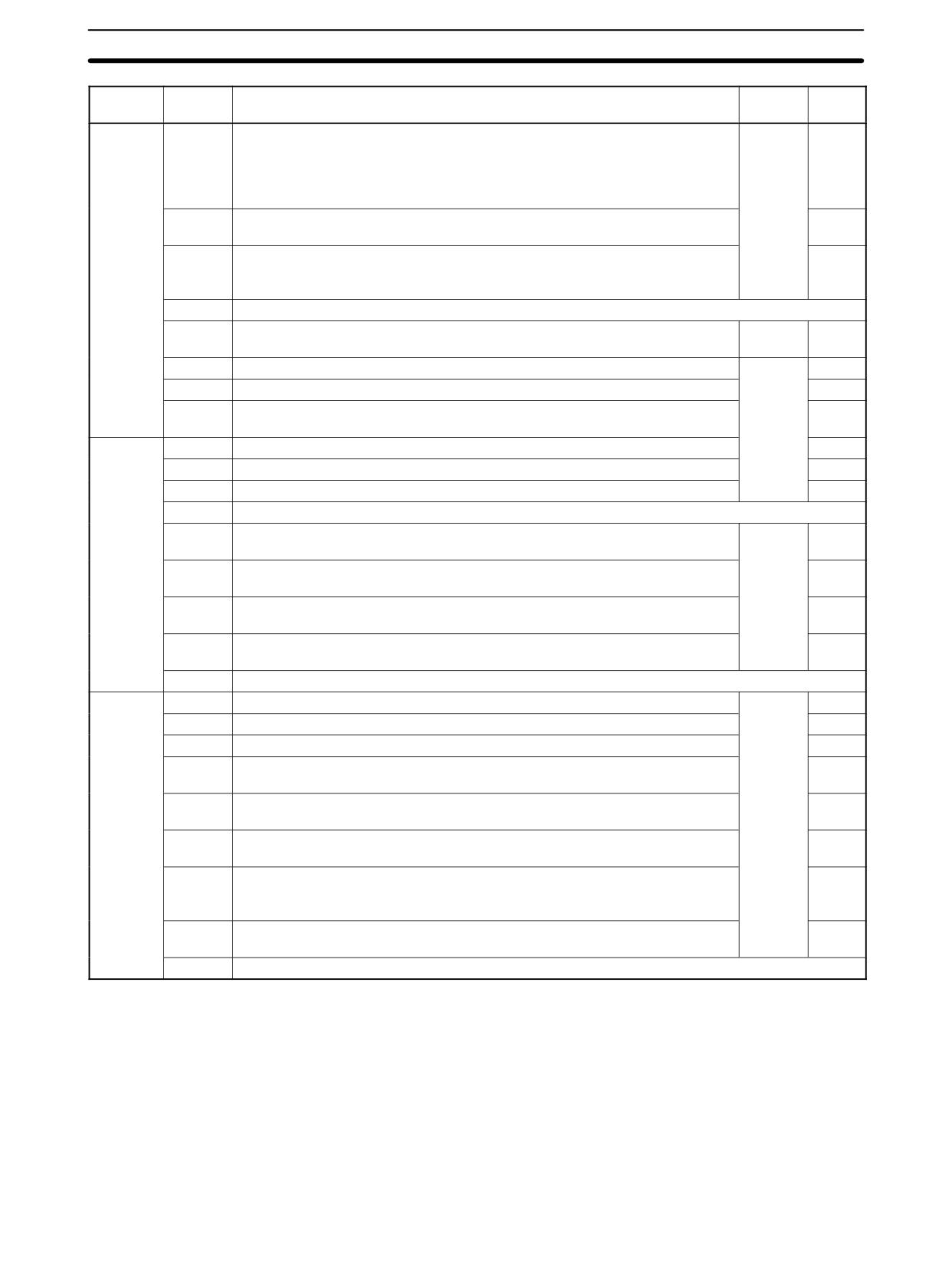
Memory Areas
Appendix C
Word(s)
Bit(s)
Function
Read/
Page
write
SR 253
00 to 07
FAL Error Code
Read-
381
The error code (a 2-digit number) is stored here when an error occurs. The
only
FAL number is stored here when FAL(06) or FALS(07) is executed. This word
is reset (to 00) by executing a FAL 00 instruction or by clearing the error from
a Programming Device.
08
Battery Error Flag
---
Turns ON when the CPU Unit backup battery’s voltage is too low.
09
Cycle Time Overrun Flag
---
Turns ON when a cycle time overrun occurs (i.e., when the cycle time ex-
ceeds 100 ms).
10,11
Not used.
12
Changing RS-232C Setup Flag
Read/
---
Turns ON when the RS-232C port’s settings are being changed.
write
13
Always ON Flag
Read-
---
only
14
Always OFF Flag
---
15
First Cycle Flag
---
Turns ON for 1 cycle at the start of operation.
SR 254
00
1-minute clock pulse (30 seconds ON; 30 seconds OFF)
---
01
0.02-second clock pulse (0.01 second ON; 0.01 second OFF)
---
02
Negative (N) Flag
---
03
Not used.
04
Overflow (OF) Flag
Read-
---
Turns ON when an overflow occurs in a signed binary calculation.
only
05
Underflow (UF) Flag
---
Turns ON when an underflow occurs in a signed binary calculation.
06
Differential Monitor Complete Flag
155
Turns ON when differential monitoring is completed.
07
STEP(08) Execution Flag
381
Turns ON for 1 cycle only at the start of process based on STEP(08).
08 to 15
Not used.
SR 255
00
0.1-second clock pulse (0.05 second ON; 0.05 second OFF)
Read-
---
only
01
0.2-second clock pulse (0.1 second ON; 0.1 second OFF)
---
02
1.0-second clock pulse (0.5 second ON; 0.5 second OFF)
---
03
Instruction Execution Error (ER) Flag
---
Turns ON when an error occurs during execution of an instruction.
04
Carry (CY) Flag
---
Turns ON when there is a carry in the results of an instruction execution.
05
Greater Than (GR) Flag
---
Turns ON when the result of a comparison operation is “greater.”
06
Equals (EQ) Flag
---
Turns ON when the result of a comparison operation is “equal,” or when the
result of an instruction execution is 0.
07
Less Than (LE) Flag
---
Turns ON when the result of a comparison operation is “less.”
08 to 15
Not used.
Note DM 6601 in the PC Setup can be set to maintain the previous status of the Forced Status Hold Bit
(SR 25211) and the I/O Hold Bit (SR 25212) when power is turned OFF. Refer to 1-1-3 CPM2A/CPM2C PC
Setup Settings for details on the PC Setup.
573
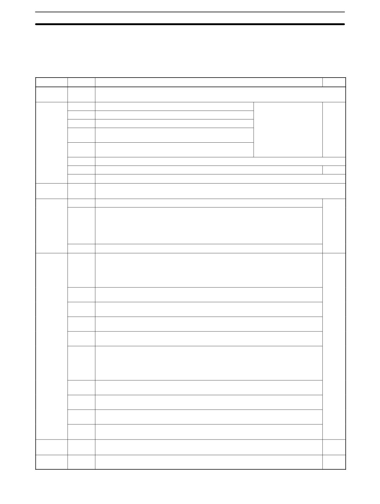
Memory Areas
Appendix C
AR Area
These bits mainly serve as flags related to CPM2A/CPM2C operation. These bits retain their status even after the
CPM2A/CPM2C power supply has been turned off or when operation begins or stops.
Word(s)
Bit(s)
Function
Page
AR 00,
00 to 15
Not used.
AR 01
AR 02
00
Expansion Unit Error Flag for 1st Unit
These flags turn ON
---
when there
is an error
in
01
Expansion Unit Error Flag for 2nd Unit
the corresponding Unit.
02
Expansion Unit Error Flag for 3rd Unit
03
Expansion Unit Error Flag for 4th Unit
(Not used by CPM2A.)
04
Expansion Unit Error Flag for 5th Unit
(Not used by CPM2A.)
05 to 07
Not used.
08 to 11
Number of Expansion Units and Expansion I/O Units Connected
---
12 to 15
Not used.
AR 03 to
00 to 15
Not used.
AR 06
AR 07
00 to 11
Not used.
---
12
Valid only for CPM2C CPU Units with lot numbers of 0190O or later. (Cannot be used
for CPM2C CPU Units with lot numbers of 3180O or earlier and cannot be used with
CPM2A CPU Units.) Refer to 1-3 Changes in SW2 for information on lot numbers.
ON: SW2 on the front of the CPU Unit is ON.
OFF: SW2 on the front of the CPU Unit is OFF.
13 to 15
Not used.
AR 08
00 to 03
RS-232C Port Error Code
246,
0: Normal completion
254
1: Parity error
2: Frame error
3: Overrun error
04
RS-232C Communications Error Flag
Turns ON when an RS-232C port communications error occurs.
05
RS-232C Transmit Ready Flag
Turns ON when the PC is ready to transmit data. (No-protocol and Host Link only)
06
RS-232C Reception Completed Flag
Turns ON when the PC has completed reading data. (No-protocol only)
07
RS-232C Reception Overflow Flag
Turns ON when an overflow has occurred. (No-protocol only)
08 to 11
Peripheral Port Error Code
0: Normal completion
1: Parity error
2: Frame error
3: Overrun error
12
Peripheral Port Communications Error Flag
Turns ON when a peripheral port communications error occurs.
13
Peripheral Port Transmit Ready Flag
Turns ON when the PC is ready to transmit data. (No-protocol and Host Link only)
14
Peripheral Port Reception Completed Flag
Turns ON when the PC has completed reading data. (No-protocol only)
15
Peripheral Port Reception Overflow Flag
Turns ON when an overflow has occurred. (No-protocol only)
AR 09
00 to 15
RS-232C Port Reception Counter (4 digits BCD)
254
Valid only when no-protocol communications are used.
AR 10
00 to 15
Peripheral Port Reception Counter (4 digits BCD)
254
Valid only when no-protocol communications are used.
574

Memory Areas
Appendix C
Word(s)
Bit(s)
Function
Page
AR 11
00 to 07
High-speed Counter Range Comparison Flags
57
00 ON: Counter PV is within comparison range 1
(Note 1)
01 ON: Counter PV is within comparison range 2
02 ON: Counter PV is within comparison range 3
03 ON: Counter PV is within comparison range 4
04 ON: Counter PV is within comparison range 5
05 ON: Counter PV is within comparison range 6
06 ON: Counter PV is within comparison range 7
07 ON: Counter PV is within comparison range 8
08
High-speed Counter Comparison Operation
ON:
Operating
OFF:
Stopped
09
High-speed Counter PV Overflow/Underflow Flag
ON:
An overflow or underflow occurred.
OFF:
Normal operation
10
Not used.
11
Pulse Output 0 Output Status
100
ON:
Pulse output 0 is accelerating or decelerating.
OFF:
Pulse output 0 is operating at a constant rate.
12
Pulse Output 0 Overflow/Underflow Flag
ON:
An overflow or underflow occurred.
OFF:
Normal operation
13
Pulse Output 0 Pulse Quantity Set Flag
ON:
Pulse quantity has been set.
OFF:
Pulse quantity has not been set.
14
Pulse Output 0 Pulse Output Completed Flag
ON:
Completed
OFF:
Not completed
15
Pulse Output 0 Output Status
ON:
Pulses being output.
OFF:
Stopped.
AR 12
00 to 11
Not used.
(Note 1)
12
Pulse Output 1 Overflow/Underflow Flag
100
ON:
An overflow or underflow occurred.
OFF:
Normal operation
13
Pulse Output 1 Pulse Quantity Set Flag
ON:
Pulse quantity has been set.
OFF:
Pulse quantity has not been set.
14
Pulse Output 1 Pulse Output Completed Flag
ON:
Completed
OFF:
Not completed
15
Pulse Output 1 Output Status
ON:
Pulses being output.
OFF:
Stopped.
575
Memory Areas
Appendix C
Word(s)
Bit(s)
Function
Page
AR 13
00
Power-up PC Setup Error Flag
549
Turns ON when there is an error in DM 6600 to DM 6614 (the part of the PC Setup area
that is read at power-up).
01
Start-up PC Setup Error Flag
Turns ON when there is an error in DM 6615 to DM 6644 (the part of the PC Setup area
that is read at the beginning of operation).
02
RUN PC Setup Error Flag
Turns ON when there is an error in DM 6645 to DM 6655 (the part of the PC Setup area
that is always read).
03, 04
Not used.
05
Cycle Time Too Long Flag
---
Turns ON if the actual cycle time is longer than the cycle time set in DM 6619.
06, 07
Not used.
08
Memory Area Specification Error Flag
---
Turns ON when a non-existent data area address is specified in the program.
09
Flash Memory Error Flag
---
Turns ON when there is an error in flash memory.
10
Read-only DM Error Flag
550
Turns ON when a checksum error occurs in the read-only DM (DM 6144 to DM 6599)
and that area is initialized.
11
PC Setup Error Flag
Turns ON when a checksum error occurs in the PC Setup area.
12
Program Error Flag
---
Turns ON when a checksum error occurs in the program memory (UM) area, or when
an improper instruction is executed.
13
Expansion Instruction Area Error Flag
Turns ON when a checksum error occurs in the expansion instruction assignments area. The
expansion instruction assignments will be cleared to their default settings.
14
Data Save Error Flag
---
Turns ON if data could not be retained with the backup battery.
The following words are normally backed up by the battery:
DM read/write words (DM 0000 to DM 1999 and DM 2022 to DM 2047), Error Log
(DM 2000 to DM 2021), HR area, counter area, SR 25511, SR 25512 (if DM 6601 is set
to hold I/O memory at startup), AR 23, operating mode (if DM 6600 is set to use the
previous operating mode), and clock words (AR 17 to AR 21, for CPU Units with
clocks).
If the above words cannot be retained, all data will be cleared except that AR 2114 will
be turned ON. The CPU Unit will start in PROGRAM mode if DM 6600 is set to use the
previous operating mode. (If DM 6604 is set to generate an error, the PC will start in
PROGRAM mode regardless.)
15
Not used.
AR 14
00 to 15
Maximum Cycle Time (4 digits BCD, see note 3)
519
The longest cycle time since the beginning of operation is stored. It is not cleared when
operation stops, but it is cleared when operation starts again.
AR 15
00 to 15
Current Cycle Time (4 digits BCD, see note 3)
The most recent cycle time during operation is stored. The Current Cycle Time is not
cleared when operation stops.
AR 16
00 to 15
Not used.
AR 17
00 to 07
Minute (00 to 59, BCD)
159
(Note 2)
08 to 15
Hour (00 to 59, BCD)
AR 18
00 to 07
Second (00 to 59, BCD)
(Note 2)
08 to 15
Minute (00 to 59, BCD)
AR 19
00 to 07
Hour (00 to 23, BCD)
(Note 2)
08 to 15
Day of the Month (01 to 31, BCD)
AR 20
00 to 07
Month (01 to 12, BCD)
(Note 2)
08 to 15
Year (00 to 99, BCD)
576
Memory Areas
Appendix C
Word(s)
Bit(s)
Function
Page
AR 21
00 to 07
Day of the Week3 (00 to 06, BCD)
159
00: Sunday
01: Monday
02: Tuesday
03: Wednesday
(Note 2)
04: Thursday
05: Friday
06: Saturday
08 to 12
Not used.
13
30-second Compensation Bit
159
Turn this bit ON to round off to the nearest minute. When the seconds are 00 to 29, the
seconds are cleared to 00 and the rest of the time setting is left unchanged. When the
seconds are 30 to 59, the seconds are cleared to 00 and the time is incremented by
one minute.
14
Clock Stop Bit
Turn this bit ON to stop the clock. The time/date can be overwritten while this bit is ON.
15
Clock Set Bit
To change the time/date, turn ON AR 2114, write the new time/date (being sure to leave
AR 2114 ON), and then turn this bit ON to enable a new time/date setting. The clock
will restart and both AR 2114 and AR 2115 will be turned OFF automatically.
AR 22
00 to 15
Not used.
AR 23
00 to 15
Power-off Counter (4 digits BCD)
---
This is the count of the number of times that the power has been turned off.
To clear the count, write “0000” from a Programming Device.
Note 1. The same data can be read immediately with PRV(62).
2. The time and date can be set while AR 2114 is ON. The new setting becomes effective when AR 2115 is
turned ON. (AR 2114 and AR 2115 are turned OFF automatically when the new setting goes into effect.)
These words will contain 0000 in CPM2C CPU Units that are not equipped with the clock function.
3. The units for the maximum and current cycle times are determined by the setting in bits 08 to 15 of
DM 6618. A setting of 00 specifies 0.1-ms units, 01 specifies 0.1-ms units, 02 specifies 1-ms units, and
03 specifies 10-ms units.
SRM1 Memory Areas
Memory Area Structure
The following memory areas can be used with the SRM1.
Data area
Words
Bits
Function
IR area1
Input area
IR 000 to IR 007
IR 00000 to IR 00715
These bits can be allocated to the external
(8 words)
(128 bits)
I/O terminals. The ON/OFF status of the I/O
bits will be the same as the ON/OFF status
of the I/O terminals
Output area
IR 010 to IR 017
IR 01000 to IR 01715
(When the CompoBus/S is used in 128-bit
(8 words)
(128 bits)
mode, IR 004 to IR 007 and IR 014 to
IR 017 can also be used as work bits.)
Work area
IR 008 to IR 009
IR 00800 to IR 00915
Work bits can be freely used within the pro-
IR 018 to IR 019
IR 01800 to IR 01915
gram. IR 232 to IR 239 however, are used
IR 200 to IR 239
IR 20000 to IR 23915
as the MACRO input area when MCRO(99)
(44 words)
(704 bits)
is being used.
SR area
SR 240 to SR 255
SR 24000 to SR 25507
These bits serve as storage space for flags
(16 words)
(248 bits)
and function set values/present values for
SRM1 operation. Refer to SR Area.
TR area
---
TR 0 to TR 7
When a complicated ladder diagram cannot
(8 bits)
be recorded as a mnemonic these bits are
used to temporarily store ON/OFF status at
program branches. These temporary bits
cannot be used within the same block but if
the blocks are different several may be
used. The ON/OFF status of these bits can-
not be monitored using the monitoring func-
tion of a Programming Device.
HR area2
HR 00 to HR 19
HR 0000 to HR 1915
These bits store data and retain their ON/
(20 words)
(320 bits)
OFF status when power is turned off, or op-
eration starts or stops. They are used in the
same way as work bits.
577

Memory Areas
Appendix C
Data area
Words
Bits
Function
AR area2
AR 00 to AR 15
AR 0000 to AR 1515
These bits serve specific functions such as
(16 words)
(256 bits)
flags and control bits. AR 04 to 07 are used
as slaves. Refer to AR Area.
LR area1
LR 00 to LR 15
LR 0000 to LR 1515
Used for a 1:1 data link with another SRM1,
(16 words)
(256 bits)
CQM1 or C200HS PC.
Timer/Counter area2
TC 000 to TC 127 (timer/counter numbers)3
Timers and counter use the TIM, TIMH(15),
CNT and CNTR(12) instructions. The same
numbers are used for both timers and
counters.
Timer/counter numbers should be specified
as bits when dealing with timer/counter
present values. The counter data will be
stored even when the SRM1 power is
turned off or operation is stopped or started.
When timer/counter are treated as up-flags
the number should be specified as relay
data.
DM area
Read/write2
DM 0000 to DM 1999
---
DM area data can be accessed in word
(2,000 words)
units only. Word values are retained when
the power is turned off, or operation started
or stopped.
Read/write areas can be read and written
freely within the program.
Error log4
DM 2000 to DM 2021
---
Used to store the time of occurrence and
(22 words)
error code of errors that occur. Refer to 7-5
Coding Right-hand Instructions.
Read-only4
DM 6144 to DM 6599
---
Cannot be overwritten from program.
(456 words)
PC Setup4
DM 6600 to DM 6655
---
Used to store various parameters that con-
(56 words)
trol PC operation.
Note 1.
IR and LR bits that are not used for their allocated functions can be used as work bits.
2.
The contents of the HR area, LR area, Counter area, and read/write DM area are backed up by a capaci-
tor. At 25_C, the capacitor will back up memory for 20 days. Refer to 2-1-2 Characteristics in the SRM1
Master Control Unit Operation Manual for a graph showing the backup time vs. temperature.
3.
When accessing a PV, TC numbers are used as word data; when accessing Completion Flags, they are
used as bit data.
4.
Data in DM 6144 to DM 6655 cannot be overwritten from the program, but they can be changed from a
Programming Device.
SR Area
These bits mainly serve as flags related to SRM1 operation or contain present and set values for various functions.
The functions of the SR area are explained in the following table.
Note “Read-only” words and bits can be read as status in controller PC operation, but they cannot be written from
the ladder program. Bits and words that are “Not used” are also read-only.
Word(s)
Bit(s)
Function
Read/
Page
write
SR 240
00 to 15
Not used.
to
SR 247
SR 248,
00 to 15
Reserved.
SR 249
SR 250,
00 to 15
Not used.
SR 251
578