FANUC I/O Unit-MODEL A. CONNECTION AND MAINTENANCE MANUAL (B-61813E/04) - page 3
5.DIGITAL INPUT/OUTPUT MODULESCONNECTION
B-61813E/04
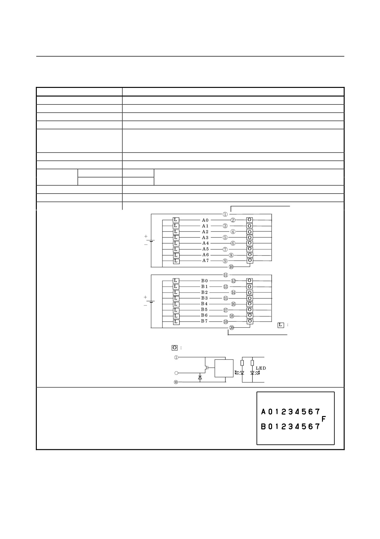
(21) Output module AOD16DP
Item
Specifications
Points/module
16 points
Points/common
8 points/common
Sink/source current
Source current type
Rated load voltage
12 to 24VDC +20%, −15%
Maximum load current
0.3A (2.4A/common)
0.5A (2A/common)
See the "Load reduction curve" shown in Fig. 5.3 (f).
Maximum voltage drop when ON
0.63V (load current ×1.25Ω)
Maximum leak current when OFF
40µA
Response time
OFF→ON
Max.2ms
This is the value from input to output in the module. The actual value is
ON→OFF
Max.2ms
determined by adding it to the scanning time depending on each system.
Output display
LED display
External connection
Connector (20 terminals, M3.5 screw terminal)
Terminal connection and circuitry
Load
Output circuit
Output terminal
Internal
circuit
• Output protection
The internal circuit of this output module can detect a load overcurrent. To
be specific, if the load current increases abnormally, for example, because
of a cable ground fault or an internal DO driver is abnormally heated for
some reason, the protection circuit for the DO driver (4-point unit) works to
keep the output of the DO driver turned off until the cause is removed.
When the overheat protection function works, the LED "F" on the module
lights.
- 58 -
B-61813E/04
CONNECTION5.DIGITAL INPUT/OUTPUT MODULES
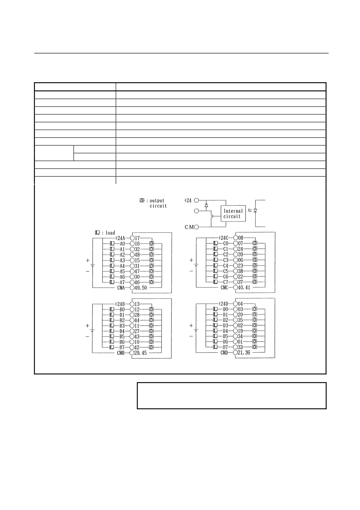
(22) Output module AOD32C1
Item
Specifications
Points/module
32 points
Points/common
8 points/common
Sink/source current
Sink current type
Rated load voltage
12 to 24VDC +20%, −15%
Maximum load current
0.3A (however 2A/common)
Maximum voltage drop when ON
0.24V (load current ×0.8Ω)
Maximum leak current when OFF
0.1mA
Response time
OFF→ON
Max.2ms
ON→OFF
Max.2ms
Output display
Not provided
External connection
Connector (HONDA TSUSHIN MR-50RMA)
Terminal connection and circuitry
NOTE
For the common (CMA, CMB, CMC, CMD), make
sure to use both of them.
- 59 -
5.DIGITAL INPUT/OUTPUT MODULESCONNECTION
B-61813E/04
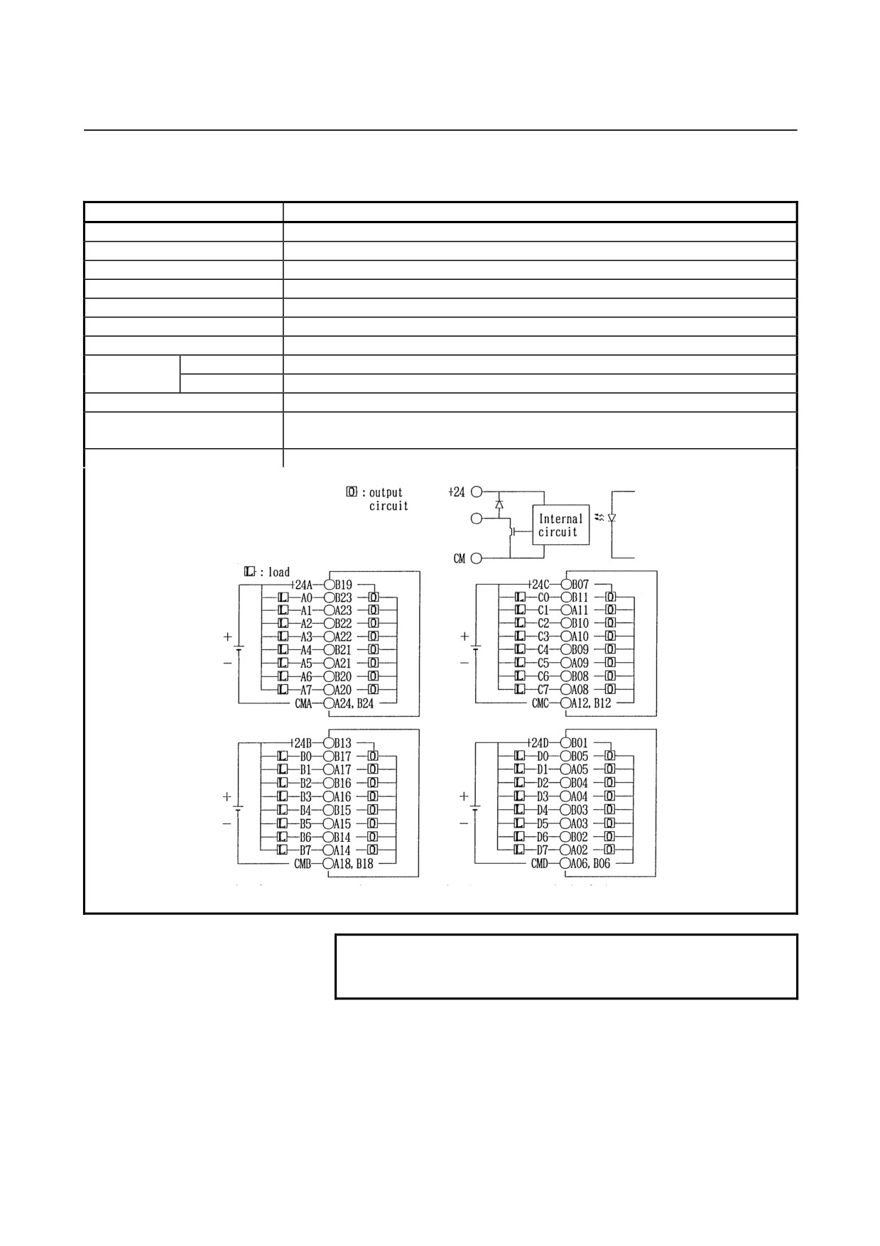
(23) Output module AOD32C2
Item
Specifications
Points/module
32 points
Points/common
8 points/common
Sink/source current
Sink current type
Rated load voltage
12 to 24VDC +20%, −15%
Maximum load current
0.3A (however 2A/common)
Maximum voltage drop when ON
0.24V (load current ×0.8Ω)
Maximum leak current when OFF
0.1mA
Response time
OFF→ON
Max.2ms
ON→OFF
Max.2ms
Output display
Not provided
External connection
Connector (HIROSE ELECTRIC HIF3BB-50PA-2.54DS in accordance with MIL
standard)
Terminal connection and circuitry
NOTE
For the common (CMA, CMB, CMC, CMD), make
sure to use both of them.
- 60 -
B-61813E/04
CONNECTION5.DIGITAL INPUT/OUTPUT MODULES
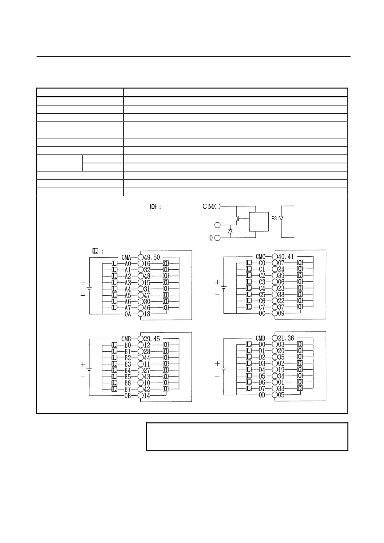
(24) Output module AOD32D1
Item
Specifications
Points/module
32 points
Points/common
8 points/common
Sink/source current
Source current type
Rated load voltage
12 to 24VDC +20%, −15%
Maximum load current
0.3A (however 2A/common)
Maximum voltage drop when ON
0.24V (load current ×0.8Ω)
Maximum leak current when OFF
0.1mA
Response Time
OFF→ON
Max.2ms
ON→OFF
Max.2ms
Output display
Not provided
External connection
Connector (HONDA TSUSHIN MR-50RMA)
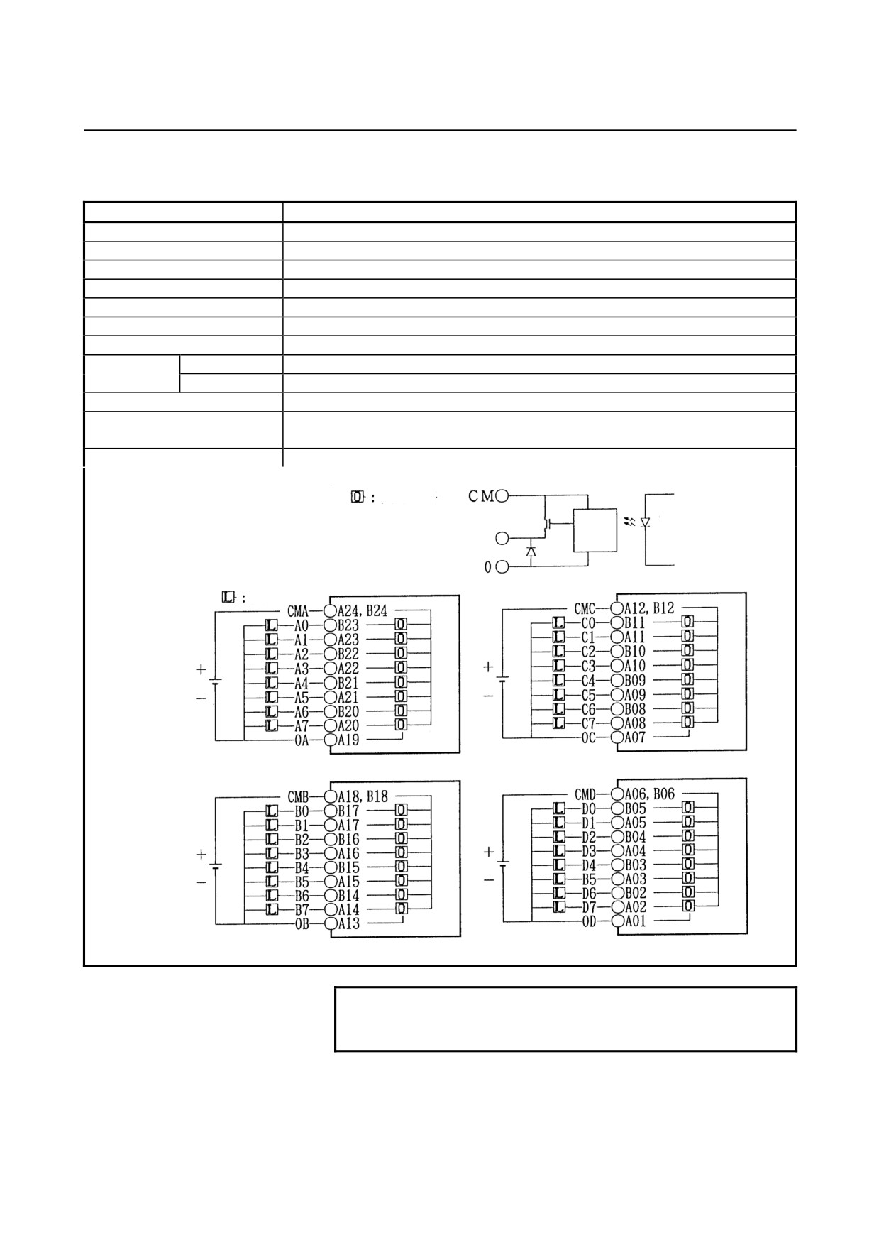
Terminal connection and circuitry
Output circuit
Internal
circuit
Load
NOTE
For the common (CMA, CMB, CMC, CMD), make
sure to use both of them.
- 61 -
5.DIGITAL INPUT/OUTPUT MODULESCONNECTION
B-61813E/04
(25) Output module AOD32D2
Item
Specifications
Points/module
32 points
Points/common
8 points/common
Sink/source current
Source current type
Rated load voltage
12 to 24VDC +20%, −15%
Maximum load current
0.3A (however 2A/common)
Maximum voltage drop when ON
0.24V (load current ×0.8Ω)
Maximum leak current when OFF
0.1mA
Response time
OFF→ON
Max.2ms
ON→OFF
Max.2ms
Output display
Not provided
External connection
Connector (HIROSE ELECTRIC HIF3BB-50PA-2.54DS in accordance with MIL
standard)
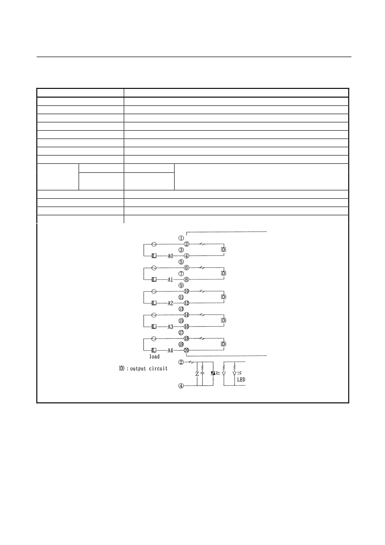
Terminal connection and circuitry
Output circuit
Internal
circuit
Load
NOTE
For the common (CMA, CMB, CMC, CMD), make
sure to use both of them.
- 62 -
B-61813E/04
CONNECTION5.DIGITAL INPUT/OUTPUT MODULES
(26) Output module AOA05E
Item
Specifications
Points/module
5 points
Points/common
1 points/common
Rated load voltage
100 to 230VAC ±15%, 47 to 63Hz
Maximum load current
2A/point (however 5A/module)
Maximum rush current
25A ( 1 period)
Limit of load
Refer to load derating curve (Fig. 5.3 (b))
Maximum voltage drop when ON
1.5Vrms
Maximum leak current when OFF
3.0mA (115VAC), 6.0mA (230VAC)
Response time
OFF→ON
Max.1ms
This is the value from input to output in the module. The actual value
ON→OFF
Half of the load
is determined by adding it to the scanning time depending on each
frequency or less
system.
Output display
LED display
External connection
Terminal block connector (20 terminals, M3.5 screw terminal)
Fuse
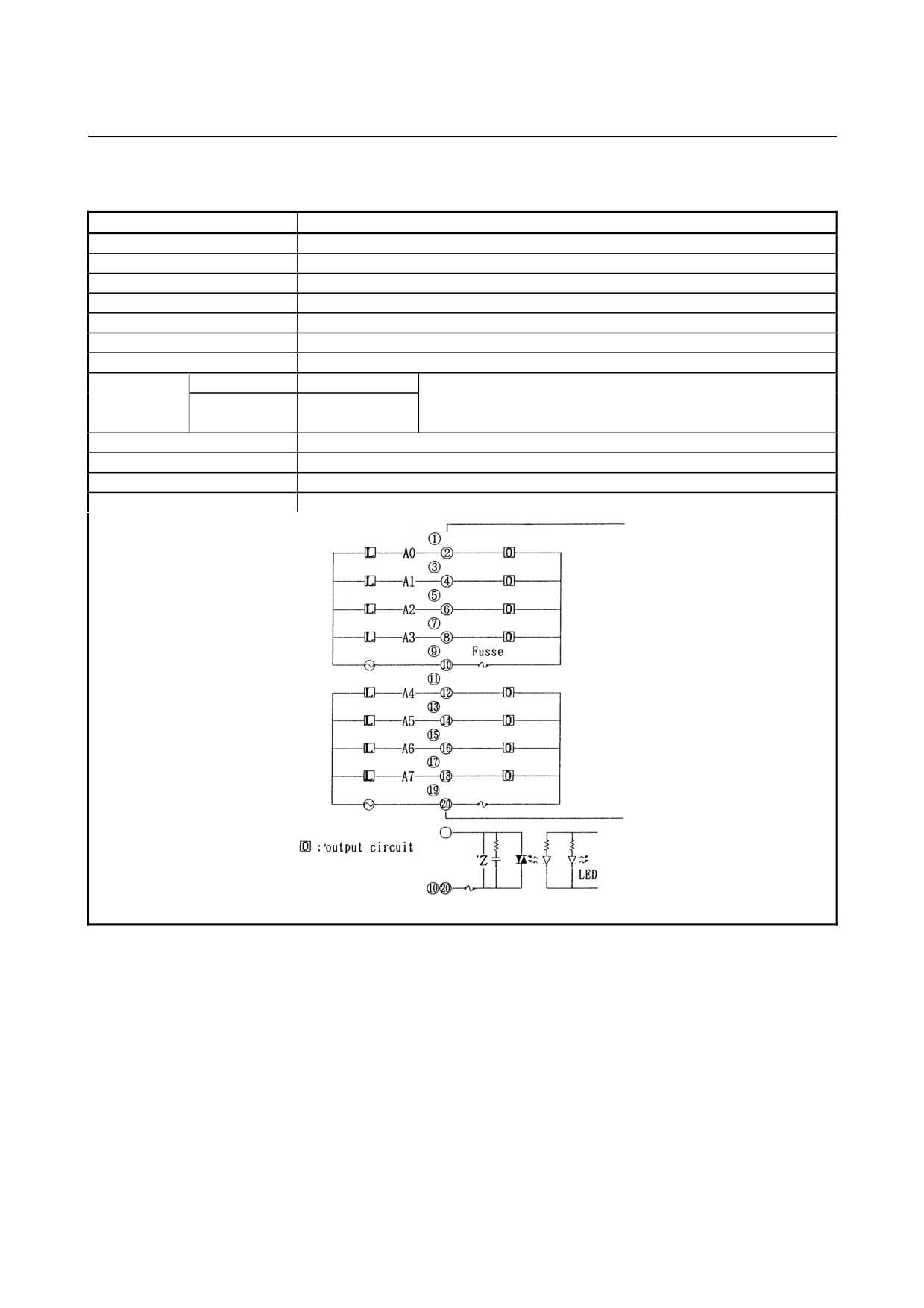
3.2A, 1 piece for each output A0 to A4
Terminal connection and circuitry
- 63 -
5.DIGITAL INPUT/OUTPUT MODULESCONNECTION
B-61813E/04
(27) Output module AOA08E
Item
Specifications
Points/module
8 points
Points/common
4 points/common
Rated load voltage
100 to 230VAC ±15%, 47 to 63Hz
Maximum load current
1A/point (however 2A/common)
Maximum in rush current
10A (1 period)
Maximum voltage drop when ON
1.5Vrms
Maximum leak current when OFF
3.0mA (115VAC), 6.0mA (230VAC)
Response time
OFF→ON
Max.1ms
This is the value from input to output in the module. The actual value
ON→OFF
Half of the load
is determined by adding it to the scanning time depending on each
frequency or less
system.
Output display
LED display
External connection
Terminal block connector (20 terminals, M3.5 screw terminal)
Fuse
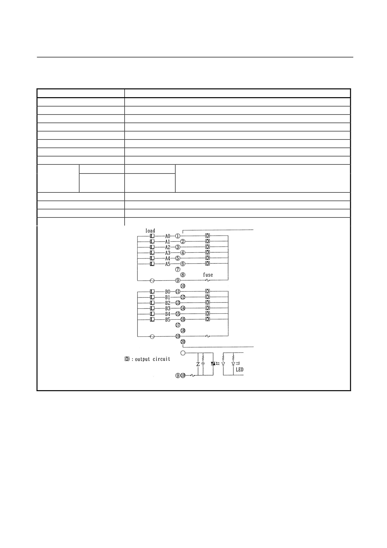
3.2A, 1 piece for each output A0 to A3 and A4 to A7
Terminal connection and circuitry
Load
- 64 -
B-61813E/04
CONNECTION5.DIGITAL INPUT/OUTPUT MODULES
(28) Output module AOA12F
Item
Specifications
Points/module
12 points
Points/common
6 points/common
Rated load voltage
100 to 115VAC ±15%, 47 to 63Hz
Maximum load current
0.5A/point (however, 2A/common)
Maximum in rush current
5A (1 period)
Limit of load
Refer to load derating curve (Fig. 5.3 (c))
Maximum voltage drop when ON
1.5Vrms
Maximum leak current when OFF
1.5mA (115VAC)
Response time
OFF→ON
Max.1ms
This is the value from input to output in the module. The actual value
ON→OFF
Half of the load
is determined by adding it to the scanning time depending on each
frequency or less
system.
Output display
LED display
External connection
Terminal block connector (20 terminals, M3.5 screw terminal)
Fuse
3.2A, 1 piece for each output A0 to A5 and B0 to B5
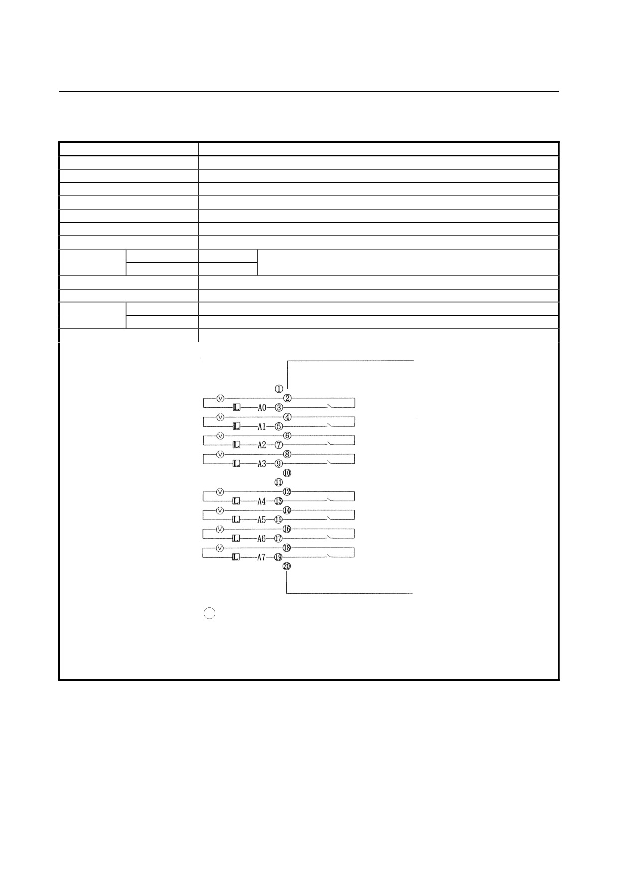
Terminal connection and circuitry
- 65 -
5.DIGITAL INPUT/OUTPUT MODULESCONNECTION
B-61813E/04
(29) Output module AOR08G
Item
Specifications
Points/module
8 points
Points/common
1 points/common
Maximum load
30VDC/250VAC, 4A (resistance load)
Minimum load
5VDC, 10mA
Limit of load
Refer to load derating curve (Fig. 5.3 (d))
Maximum voltage drop when ON
1.5Vrms
Maximum leak current when OFF
1.5mA (115VAC)
Response time
OFF→ON
Max.15ms
This is the value from input to output in the module. The actual value is
ON→OFF
Max.15ms
determined by adding it to the scanning time depending on each system.
Output display
LED display
External connection
Terminal block connector (20 terminals, M3.5 screw terminal)
Relay life
Mechanical
Min. 20,000,000 times
Electrical
Min. 100,000 times (resistance load)
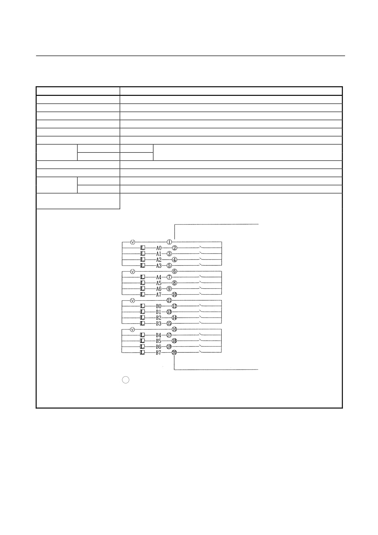
Terminal connection and circuitry
V : Direct current power or alternating current power
- 66 -
B-61813E/04
CONNECTION5.DIGITAL INPUT/OUTPUT MODULES
(30) Output module AOR16G
Item
Specifications
Points/module
16 points
Points/common
4 points/common
Maximum load
30VDC/250VAC, 2A (resistance load)
Minimum load
5VDC, 10mA
Maximum current
4A/common
Limit of load
Refer to load derating curve (Fig. 5.3 (e))
Response time
OFF→ON
Max.15ms
This is the value from input to output in the module. The actual value is
ON→OFF
Max.15ms
determined by adding it to the scanning time depending on each system.
Output display
LED display
External connection
Terminal block connector (20 terminals, M3.5 screw terminal)
Relay life
Mechanical
Min. 20,000,000 times
Electrical
Min. 100,000 times (resistance load)
Terminal connection and
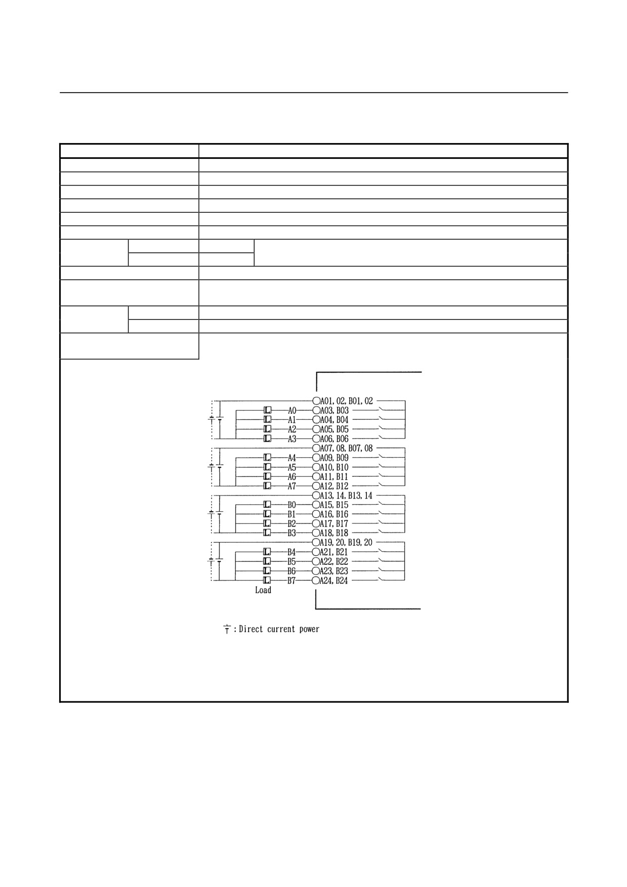
circuitry
Load
V : Direct current power or alternating current power
- 67 -
5.DIGITAL INPUT/OUTPUT MODULESCONNECTION
B-61813E/04
(31) Output module AOR16H2
Item
Specifications
Points/module
16 points
Points/common
4 points/common
Maximum load
30VDC, 2A (resistance load)
Minimum load
5VDC, 10mA
Maximum current
4A/common
Limit of load
Refer to load derating curve (Fig. 5.3 (e))
Response time
OFF→ON
Max.15ms
This is the value from input to output in the module. The actual value is
ON→OFF
Max.15ms
determined by adding it to the scanning time depending on each system.
Output display
LED display
External connection
Connector (HIROSE ELECTRIC HIF3BB-50PA-2.54DS in accordance with MIL
standard)
Relay life
Mechanical
Min. 20,000,000 times
Electrical
Min. 100,000 times (resistance load)
Terminal connection and
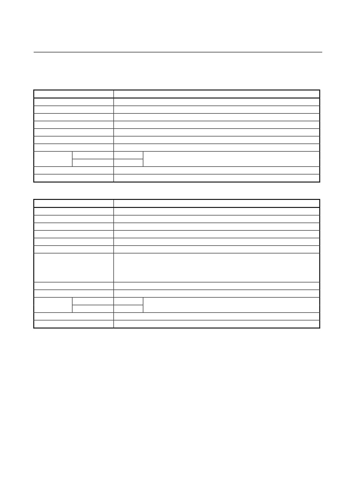
circuitry
- 68 -
B-61813E/04
CONNECTION5.DIGITAL INPUT/OUTPUT MODULES
(32) Input/output module AIO40A
- Input specifications
Item
Specifications
Points/module
24 points
Points/common
24 points/common
Sink/source current
Both directions
Input voltage
24VDC +10%, −20%
Input current
7.5mA (average)
ON voltage, current
Min. 18VDC, min. 6mA
OFF voltage, current
Max. 6VDC, max. 1.5mA
Response time
OFF→ON
Max.20ms
This is the value from input to output in the module. The actual value is
ON→OFF
Max.20ms
determined by adding it to the scanning time depending on each system.
Input display
Not provided
External connection
Connector (HONDA TSUSHIN MR-50RMA, shared by output signals)
- Output specifications
Item
Specifications
Points/module
16 points
Points/common
16 points/common
Sink/source current
Sink current type
Rated load voltage
24VDC +20%, −15%
Maximum load current
0.2A (however 2A/common)
Maximum in rush current
0.2A
Limit of load
• If the output current per point is 0.1 A or lower, all of the 16 points E0 to E7 and F0 to
F7 can be turned on at a time.
• If the output current per point is higher than 0.1 A but not higher than 0.2 A, do not
turn on more than 3 points at a time.
Maximum voltage drop when ON
1.5V
Maximum leak current when OFF
1.0mA (30VDC)
Response time
OFF→ON
Max.1ms
This is the value from input to output in the module. The actual value is
ON→OFF
Max.1ms
determined by adding it to the scanning time depending on each system.
Output display
Not provided
External connection
Connector (HONDA TSUSHIN MR-50RMA, shared by input signals)
- 69 -
5.DIGITAL INPUT/OUTPUT MODULESCONNECTION
B-61813E/04
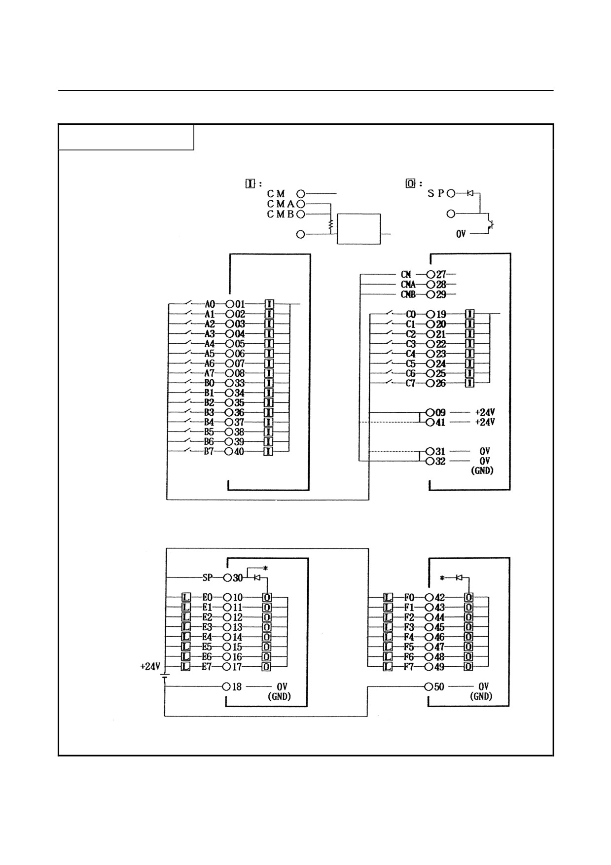
•Input/output module
Terminal connection and
circuitry
To the automatic
Input circuit
polarity
Output circuit
discrimination
circuit
Input section
Internal
circuit
Either 24 V or 0 V can be selected as an input common potential as shown above.
(Solid line: 24-V common. Dotted line: 0-V common.)
Output section
- 70 -
B-61813E/04
CONNECTION5.DIGITAL INPUT/OUTPUT MODULES
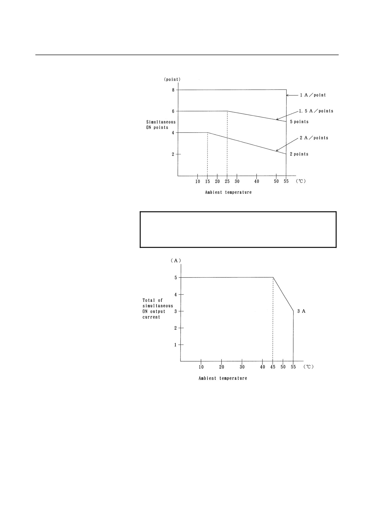
Fig.5.3 (a) AOD08D Load reduction curve
NOTE
Ambient temperature means the temperature
surrounding the I/O Unit and not that surrounding the
cabinet containing the I/O Unit.
Fig.5.3 (b) AOA05E Load reduction curve
- 71 -
5.DIGITAL INPUT/OUTPUT MODULESCONNECTION
B-61813E/04
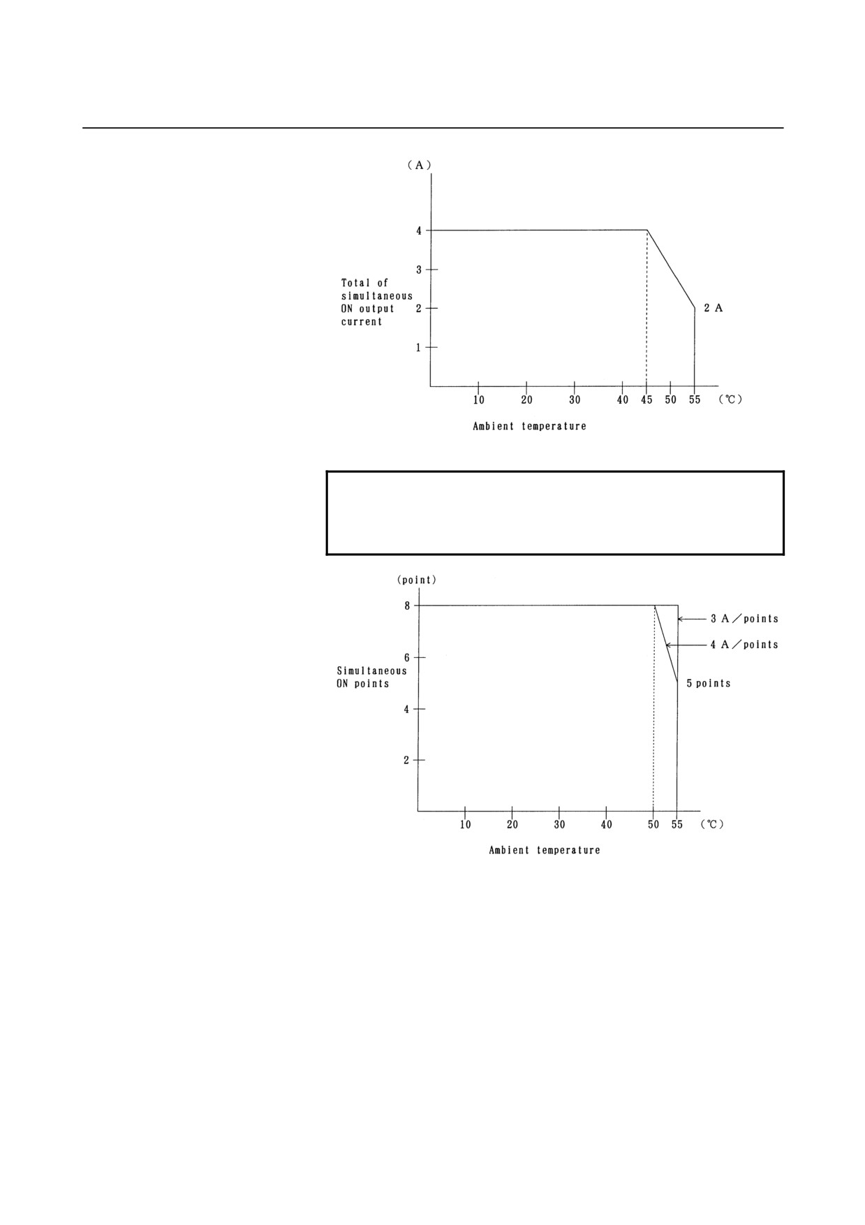
Fig.5.3 (c) AOA12F Load reduction curve
NOTE
Ambient temperature means the temperature
surrounding the I/O Unit and not that surrounding the
cabinet containing the I/O Unit.
Fig.5.3 (d) AOR08G Load reduction curve
- 72 -
B-61813E/04
CONNECTION5.DIGITAL INPUT/OUTPUT MODULES
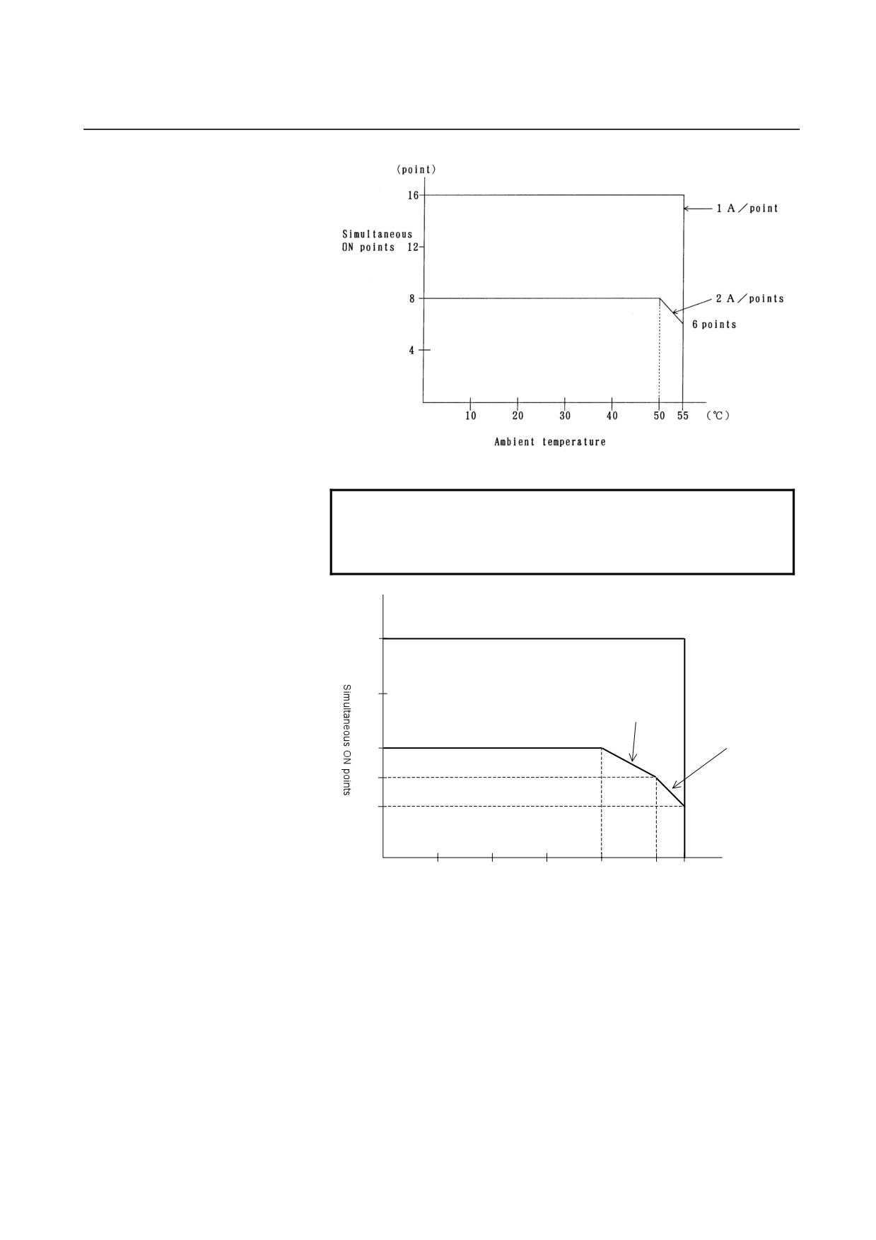
Fig.5.3 (e) AOR16G, AOR16H2 Load reduction curve
NOTE
Ambient temperature means the temperature
surrounding the I/O Unit and not that surrounding the
cabinet containing the I/O Unit.
(Point)
0.3A /points
16
12
0.5A /points (1.5A/common)
0.5A /points
0.5A /points (2A/common)
(1A/common)
8
6
4
10
20
30
40
50
55
(°C)
Ambient temperature
Fig.5.3 (f) AOD16DP Load reduction curve
- 73 -
5.DIGITAL INPUT/OUTPUT MODULESCONNECTION
B-61813E/04
5.4
DETAILS OF I/O Unit CONNECTORS (HONDA
TSUSHIN/HIROSE ELECTRIC) AND TERMINAL BLOCK
(WEIDMÜLLER)
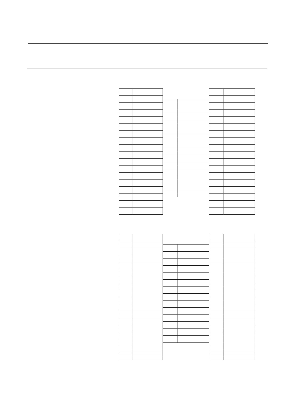
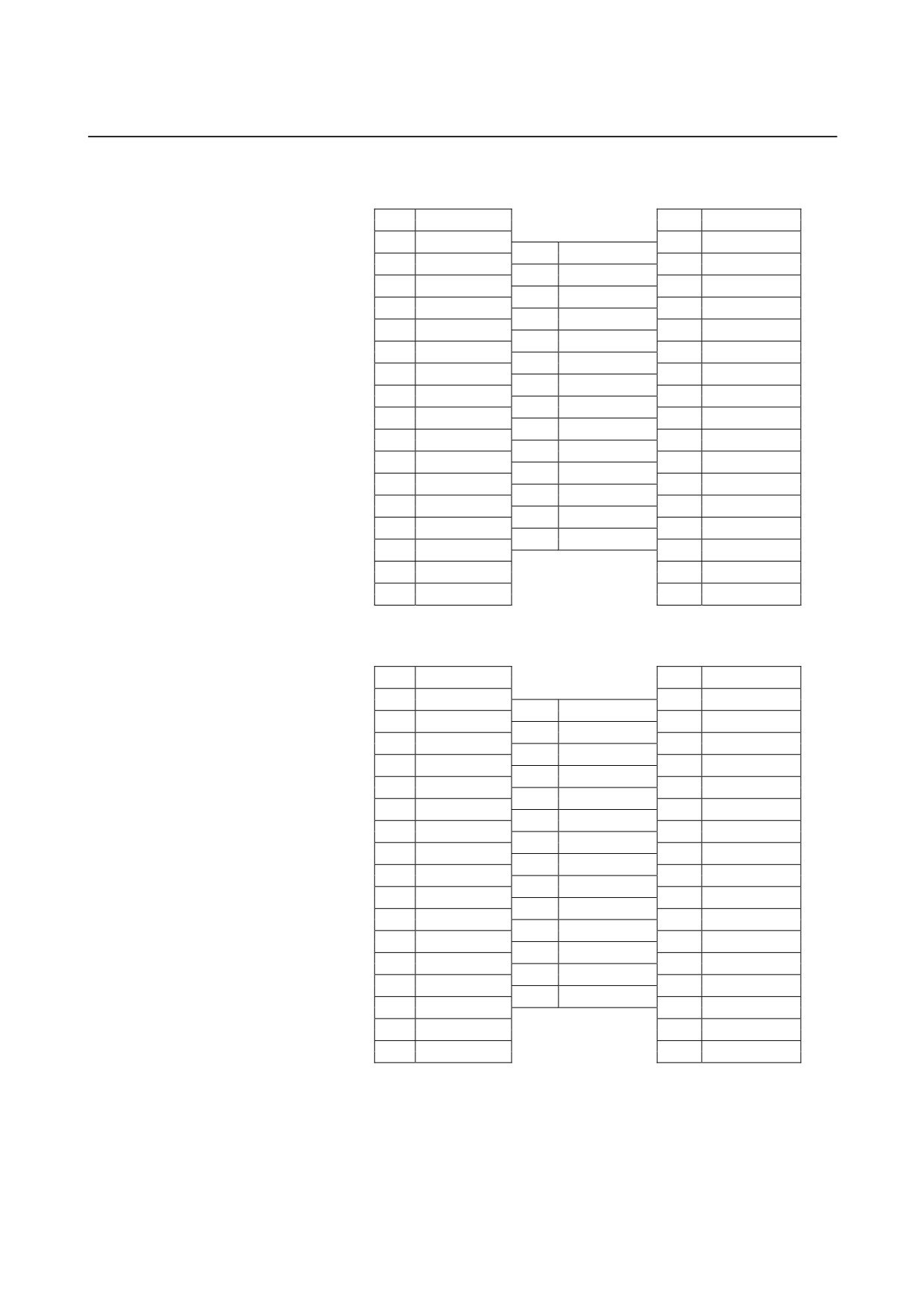
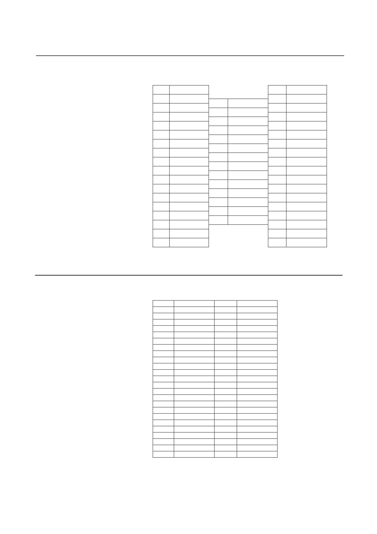
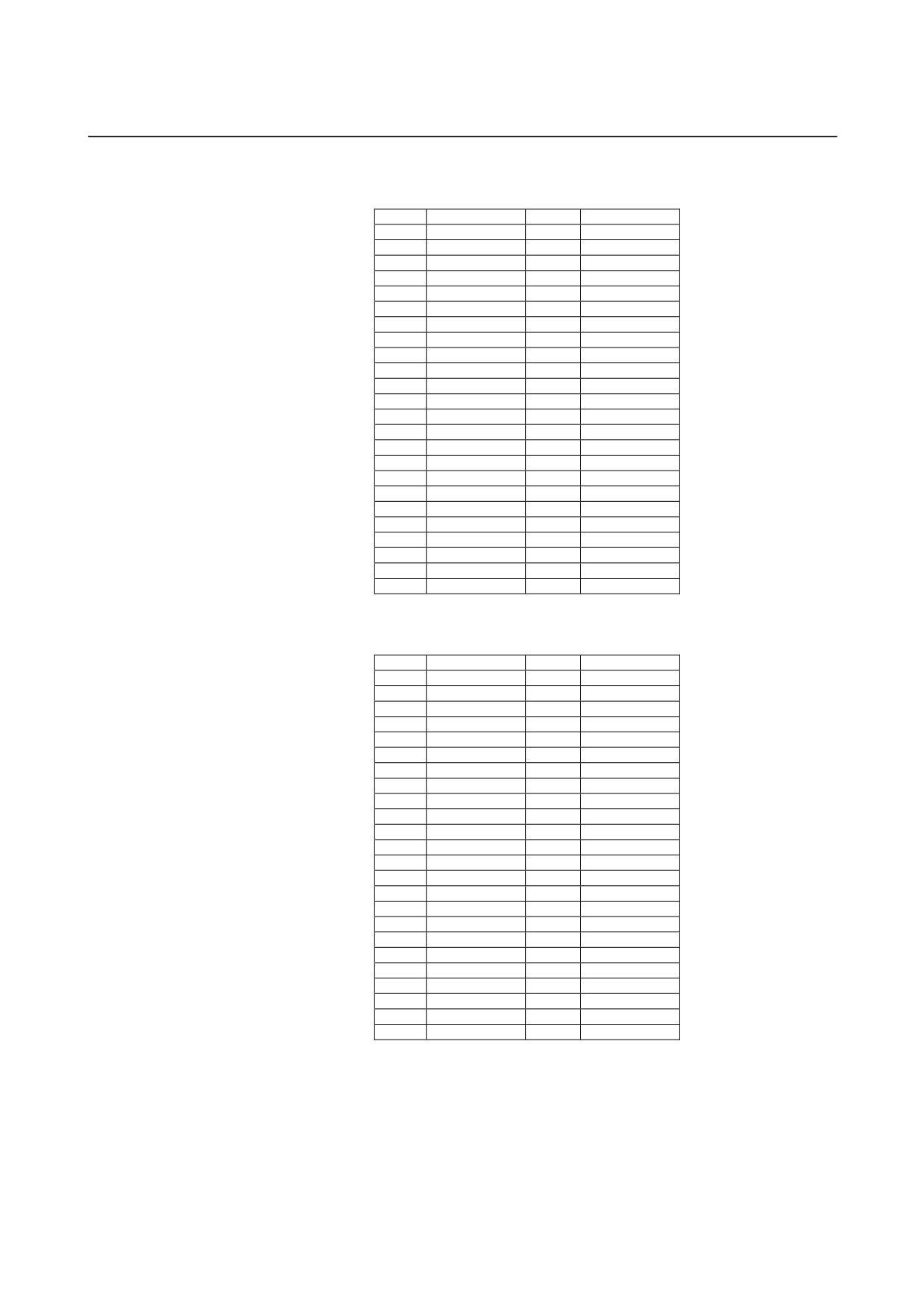
Given below are the details (signal arrangement diagrams as viewed
from the front of the module) of the connector pins and AOD16D3
terminal block for the I/O Units (32-point input module, 32-point
output module, and 24-point input/16-point output hybrid module)
explained in Section 5.3.
- 74 -
B-61813E/04
CONNECTION5.DIGITAL INPUT/OUTPUT MODULES
5.4.1
Modules Using the MR-50RMA Connector Manufactured by
Honda Tsushin
•
AID32A1/AID32B1/AID32H1 (32-point DC input module)
33
D7
01
D6
34
D5
02
D3
19
D4
35
D2
03
D0
20
D1
36
CMC
04
+24V
21
CMC
37
C7
05
GND
22
C6
38
C5
06
C3
23
C4
39
C2
07
C0
24
C1
40
CMC
08
+24V
25
41
CMC
09
GND
26
42
B7
10
B6
27
B4
43
B5
11
B3
28
B1
44
B2
12
B0
29
CMA
45
CMA
13
+24V
30
A6
46
A7
14
GND
31
A4
47
A5
15
A3
32
A1
48
A2
16
A0
49
CMA
17
+24V
50
CMA
18
GND
•
AID32E1/AID32F1 (32-point DC input module)
33
D7
01
D6
34
D5
02
D3
19
D4
35
D2
03
D0
20
D1
36
CMD
04
21
CMD
37
C7
05
22
C6
38
C5
06
C3
23
C4
39
C2
07
C0
24
C1
40
CMC
08
25
41
CMC
09
26
42
B7
10
B6
27
B4
43
B5
11
B3
28
B1
44
B2
12
B0
29
CMB
45
CMB
13
30
A6
46
A7
14
31
A4
47
A5
15
A3
32
A1
48
A2
16
A0
49
CMA
17
50
CMA
18
- 75 -
5.DIGITAL INPUT/OUTPUT MODULESCONNECTION
B-61813E/04
•
AOD32A1/AOD32C1 (32-point DC output module)
33
D7
01
D6
34
D5
02
D3
19
D4
35
D2
03
D0
20
D1
36
CMD
04
+24V-D
21
CMD
37
C7
05
22
C6
38
C5
06
C3
23
C4
39
C2
07
C0
24
C1
40
CMC
08
+24V-C
25
41
CMC
09
26
42
B7
10
B6
27
B4
43
B5
11
B3
28
B1
44
B2
12
B0
29
CMB
45
CMB
13
+24V-B
30
A6
46
A7
14
31
A4
47
A5
15
A3
32
A1
48
A2
16
A0
49
CMA
17
+24V-A
50
CMA
18
•
AOD32D1 (32-point DC output module)
33
D7
01
D6
34
D5
02
D3
19
D4
35
D2
03
D0
20
D1
36
CMD
04
21
CMD
37
C7
05
0V-D
22
C6
38
C5
06
C3
23
C4
39
C2
07
C0
24
C1
40
CMC
08
25
41
CMC
09
0V-C
26
42
B7
10
B6
27
B4
43
B5
11
B3
28
B1
44
B2
12
B0
29
CMB
45
CMB
13
30
A6
46
A7
14
0V-B
31
A4
47
A5
15
A3
32
A1
48
A2
16
A0
49
CMA
17
50
CMA
18
0V-A
- 76 -
B-61813E/04
CONNECTION5.DIGITAL INPUT/OUTPUT MODULES
• AIO40A (24-point DC input/16-point DC output hybrid module)
33
B0
01
A0
34
B1
02
A1
19
C0
35
B2
03
A2
20
C1
36
B3
04
A3
21
C2
37
B4
05
A4
22
C3
38
B5
06
A5
23
C4
39
B6
07
A6
24
C5
40
B7
08
A7
25
C6
41
+24V
09
+24V
26
C7
42
F0
10
E0
27
CM
43
F1
11
E1
28
CMA
44
F2
12
E2
29
CMA
45
F3
13
E3
30
SP
46
F4
14
E4
31
0V
47
F5
15
E5
32
0V
48
F6
16
E6
49
F7
17
E7
50
0V
18
0V
5.4.2
Modules Using the HIF3BB-50PA-2.54DS Connector
Manufactured by Hirose Electric
• AID32E2/AID32F2 (32-point DC input module)
A01
B01
A02
D7
B02
D6
A03
D5
B03
D4
A04
D3
B04
D2
A05
D1
B05
D0
A06
CMD
B06
CMD
A07
B07
A08
C7
B08
C6
A09
C5
B09
C4
A10
C3
B10
C2
A11
C1
B11
C0
A12
CMC
B12
CMC
A13
B13
A14
B7
B14
B6
A15
B5
B15
B4
A16
B3
B16
B2
A17
B1
B17
B0
A18
CMB
B18
CMB
A19
B19
A20
A7
B20
A6
A21
A5
B21
A4
A22
A3
B22
A2
A23
A1
B23
A0
A24
CMA
B24
CMA
A25
B25
- 77 -
5.DIGITAL INPUT/OUTPUT MODULESCONNECTION
B-61813E/04
•
AOD32C2 (32-point DC output module)
A01
B01
+24V-D
A02
D7
B02
D6
A03
D5
B03
D4
A04
D3
B04
D2
A05
D1
B05
D0
A06
CMD
B06
CMD
A07
B07
+24V-C
A08
C7
B08
C6
A09
C5
B09
C4
A10
C3
B10
C2
A11
C1
B11
C0
A12
CMC
B12
CMC
A13
B13
+24V-B
A14
B7
B14
B6
A15
B5
B15
B4
A16
B3
B16
B2
A17
B1
B17
B0
A18
CMB
B18
CMB
A19
B19
+24V-A
A20
A7
B20
A6
A21
A5
B21
A4
A22
A3
B22
A2
A23
A1
B23
A0
A24
CMA
B24
CMA
A25
B25
•
AOD32D2 (32-point DC output module)
A01
0V-D
B01
A02
D7
B02
D6
A03
D5
B03
D4
A04
D3
B04
D2
A05
D1
B05
D0
A06
CMD
B06
CMD
A07
0V-C
B07
A08
C7
B08
C6
A09
C5
B09
C4
A10
C3
B10
C2
A11
C1
B11
C0
A12
CMC
B12
CMC
A13
0V-B
B13
A14
B7
B14
B6
A15
B5
B15
B4
A16
B3
B16
B2
A17
B1
B17
B0
A18
CMB
B18
CMB
A19
0V-A
B19
A20
A7
B20
A6
A21
A5
B21
A4
A22
A3
B22
A2
A23
A1
B23
A0
A24
CMA
B24
CMA
A25
B25
- 78 -
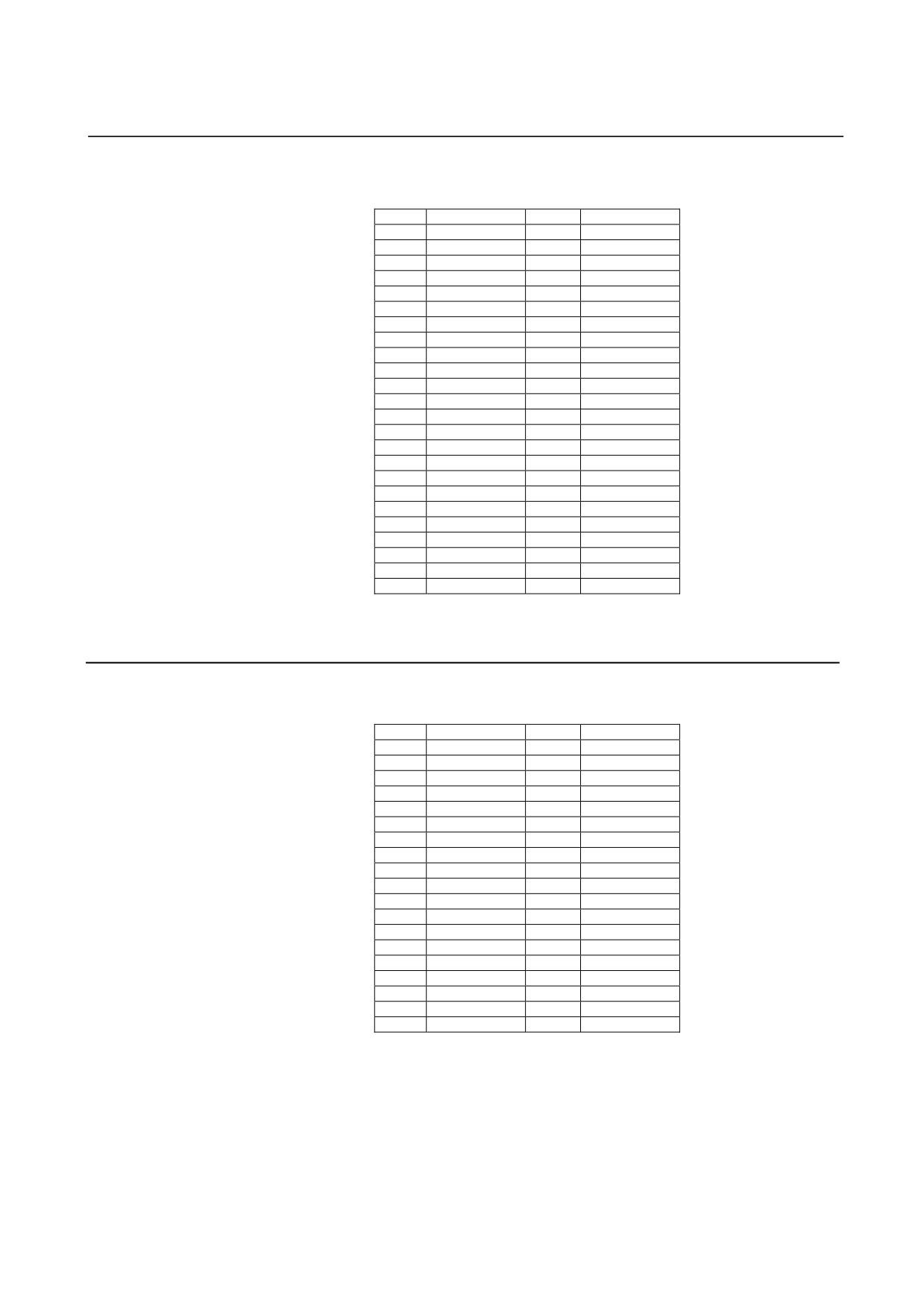
B-61813E/04
CONNECTION5.DIGITAL INPUT/OUTPUT MODULES
• AOR16H2 (16-point relay output module)
A01
CMA
B01
CMA
A02
CMA
B02
CMA
A03
A0
B03
A0
A04
A1
B04
A1
A05
A2
B05
A2
A06
A3
B06
A3
A07
CMB
B07
CMB
A08
CMB
B08
CMB
A09
A4
B09
A4
A10
A5
B10
A5
A11
A6
B11
A6
A12
A7
B12
A7
A13
CMC
B13
CMC
A14
CMC
B14
CMC
A15
B0
B15
B0
A16
B1
B16
B1
A17
B2
B17
B2
A18
B3
B18
B3
A19
CMD
B19
CMD
A20
CMD
B20
CMD
A21
B4
B21
B4
A22
B5
B22
B5
A23
B6
B23
B6
A24
B7
B24
B7
A25
B25
5.4.3
Modules Using the HIF4-40P-3.18DS Connector Manufactured
by Hirose Electric
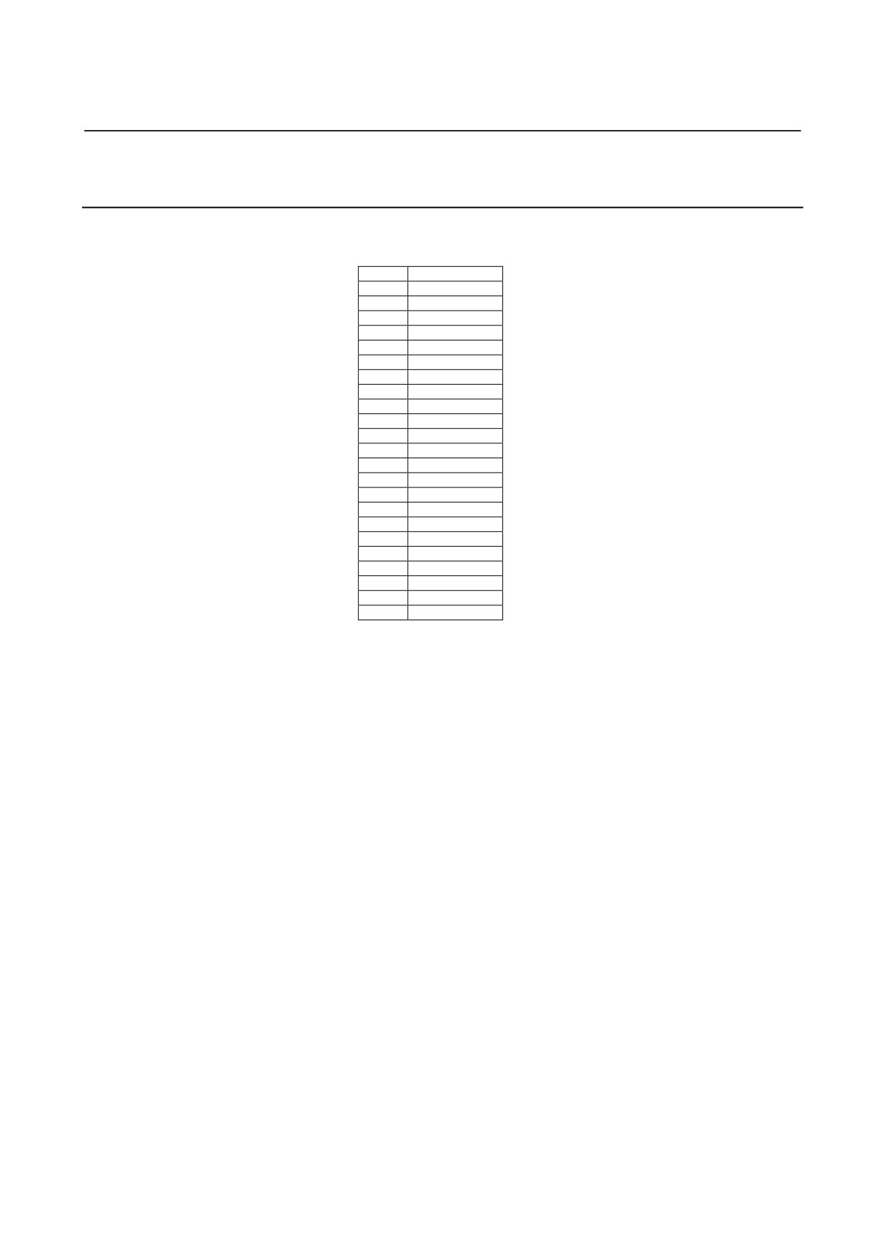
• AOD16D2 (16-point DC output module)
A01
A0
B01
0V-A
A02
A1
B02
0V-A
A03
A2
B03
CMA
A04
A3
B04
CMA
A05
CMA
B05
CMA
A06
A4
B06
0V-B
A07
A5
B07
0V-B
A08
A6
B08
CMB
A09
A7
B09
CMB
A10
CMB
B10
CMB
A11
CMC
B11
CMC
A12
B0
B12
CMC
A13
B1
B13
CMC
A14
B2
B14
0V-C
A15
B3
B15
0V-C
A16
CMD
B16
CMD
A17
B4
B17
CMD
A18
B5
B18
CMD
A19
B6
B19
0V-D
A20
B7
B20
0V-D
- 79 -
5.DIGITAL INPUT/OUTPUT MODULESCONNECTION
B-61813E/04
5.4.4
Modules Using the Terminal Block BL3.5/24/90F Manufactured
by Weidmüller
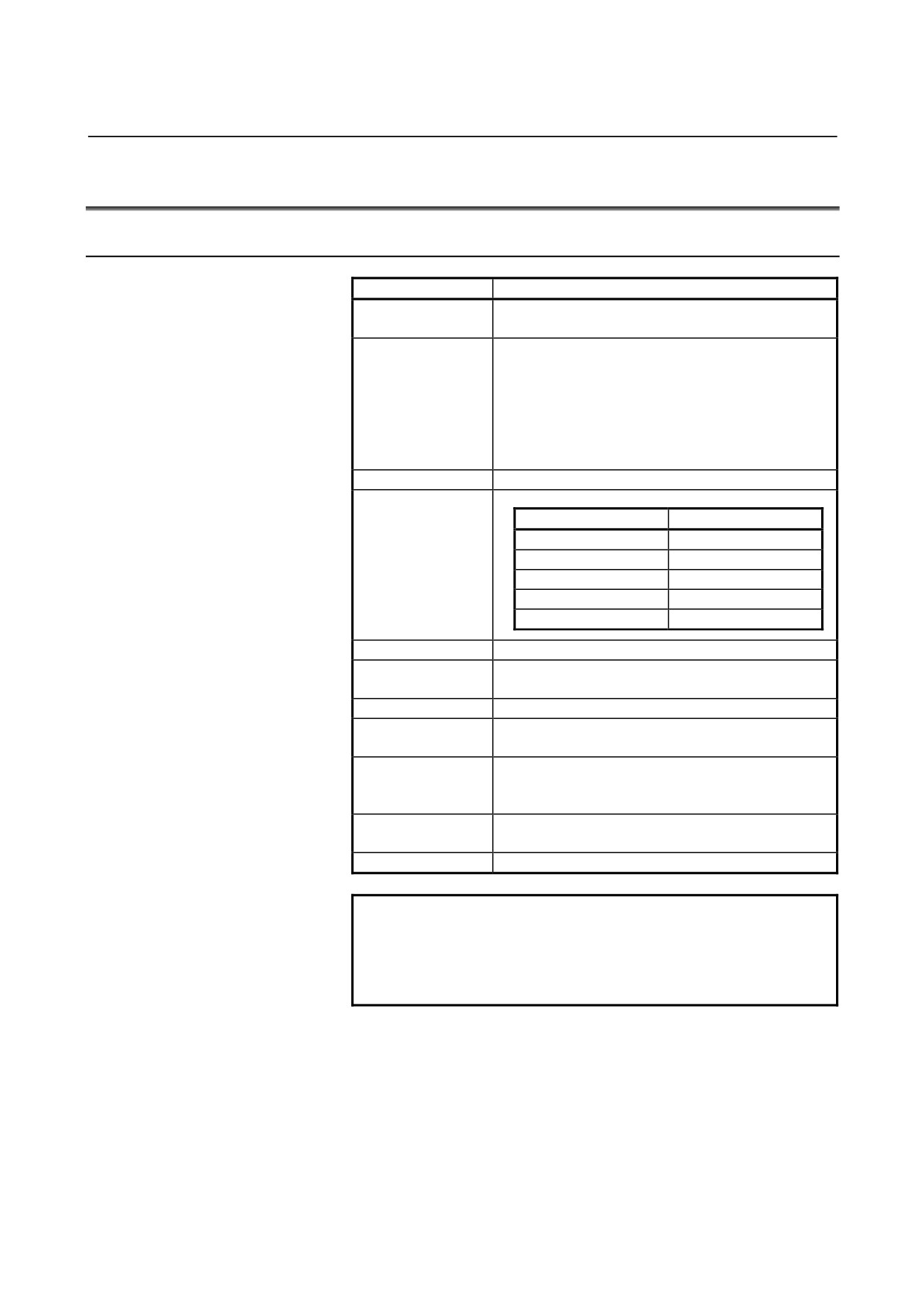
• AOD16D3 (16-point DC output module)
01
CMA
02
A0
03
A1
04
A2
05
A3
06
0V-A
07
CMB
08
A4
09
A5
10
A6
11
A7
12
0V-B
13
CMC
14
B0
15
B1
16
B2
17
B3
18
0V-C
19
CMD
20
B4
21
B5
22
B6
23
B7
24
0V-D
- 80 -
6.ANALOG INPUT MODULE
CONNECTION
B-61813E/04
6.1
12-BIT ANALOG INPUT MODULE (AAD04A)
6.1.1
Specifications
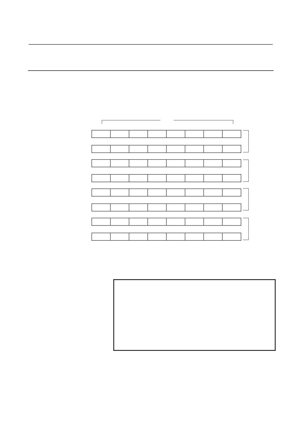
Item
Specifications
Number of input
4 channel/module
channel
Analog input
• Voltage input
-10VDC to+10VDC(input resistance 4.7MΩ)
• Current input
-20mADC to+20mADC(input resistance 250Ω)
Caution) Which method to use, voltage input or current
input, can be selected by connecting the
corresponding input to the terminal block.
Digital output
12 bit binary (complementary representation of "2".)
Input/output
correspondence
Analog input
Digital output
+10V
+2000
+5V or + 20mA
+1000
0V or 0mA
0
-5V or -20mA
-1000
-10V
-2000
Resolution
5mV or 20µA
Total precision
Voltage input ±0.5%(For full scale)
Current input ±1%(For full scale)
Conversionary time
Max.2ms (Note)
Maximum input
±15V, ±30mA
voltage/current
Isolation
Photocoupler isolated (between the input signal and the
base)
However, not isolated between input channels
Output connecting
Removable terminal block (20 terminals, M3.5 screw
terminal)
Required input points
64 points
NOTE
Conversion time means that only in a module.
Actual response speed is determined by adding the
scanning time depending on each system to this
conversion time.
- 82 -
B-61813E/04
CONNECTION
6.ANALOG INPUT MODULE
6.1.2
Correspondence between Input Signals and Addresses in a
Module
In the analog input module AAD04A, the 4-channel analog input
signals are cyclically A-D converted in order, and the converted digital
data are written in the following addresses. Therefore, in the PMC
program, it is possible at any time to know the values for the analog
input signals by referring to the following addresses.
Address
Bits
in module
7
6
5
4
3
2
1
0
0
D07-0
D06-0
D05-0
D04-0
D03-0
D02-0
D01-0
D00-0
Channel 0
1
X-0
X-0
X-0
X-0
D11-0
D10-0
D09-0
D08-0
2
D07-1
D06-1
D05-1
D04-1
D03-1
D02-1
D01-1
D00-1
Channel 1
3
X-1
X-1
X-1
X-1
D11-1
D10-1
D09-1
D08-1
4
D07-2
D06-2
D05-2
D04-2
D03-2
D02-2
D01-2
D00-2
Channel 2
5
X-2
X-2
X-2
X-2
D11-2
D10-2
D09-2
D08-2
6
D07-3
D06-3
D05-3
D04-3
D03-3
D02-3
D01-3
D00-3
Channel 3
7
X-3
X-3
X-3
X-3
D11-3
D10-3
D09-3
D08-3
D00-n and D11-n correspond to the weights of 20 and 211 respectively.
Here, D11-n corresponds to the sign bit in the complementary
representation of "2."
In addition, in X-n is written the same value as that in D11-n.
NOTE
1 When addressing I/O modules, the beginning
address for this module should be assigned to an
even one. Moreover, when an A-D converted value is
referred to in a PMC program, make sure to read the
data in unit of a word (16 bits).
2 Note that on the PMC-N, -NA, and -QA (PMC for the
Series 15 and F-D Mate), the high-order one byte and
low-order one byte of a word (16 bits) are
interchanged with each other as described below.
- 83 -
6.ANALOG INPUT MODULE
CONNECTION
B-61813E/04
Addresses for word-unit operation in the PMC-N, NA, and QA
Analog input module → PMC
Address in the
module
High-order byte
Low-order byte
Channel 0
0
D07-0 to D00-0
X-0,D11-0 to D08-0
Channel 1
+2
D07-1 to D00-1
X-1,D11-1 to D08-1
Channel 2
+4
D07-2 to D00-2
X-2,D11-2 to D08-2
Channel 3
+6
D07-3 to D00-3
X-3,D11-3 to D08-3
- 84 -
B-61813E/04
CONNECTION
6.ANALOG INPUT MODULE
6.1.3
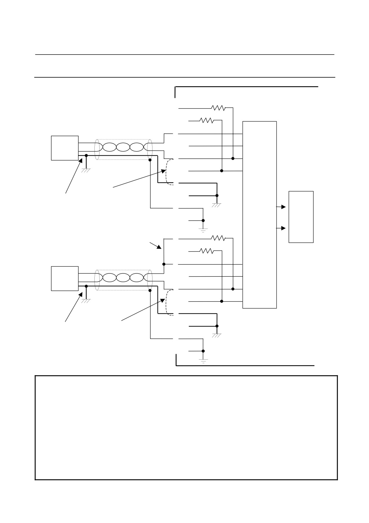
Connecting with Analog Input Module
Analog input module (AAD04A)
I0+
①
I1+
250Ω
②
Voltage input (channel0)
③
Voltage
+
V1+
supply
④
-
V0-
GND
⑤
V1-
Multi
⑥
processor
COM0
⑦
Note
COM1
Note
4-2
⑧
AD
4-1
FG0
converter
⑨
FG1
⑩
I2+
250Ω
Note 2
⑪
I3+
⑫
V2+
Current input (channel 2)
⑬
Current
+
V3+
supply
⑭
-
V2-
GND
⑮
V3-
⑯
COM2
⑰
COM3
Note
Note
⑱
4-1
4-2
FG2
⑲
FG3
⑳
NOTE
1 Though the example above shows the connection of channels 0 and 2, it is just the
same with the channel 1 (I1+, V1+, V1-, COM1 and FG1) and the channel 3 (I3+, V3+,
V3-, COM3 and FG3).
2 Either voltage input or current input can be specified for each channel. When current
input is specified, make sure to short-circuit in + and Vn+ (n: 0 to 3).
3 Use shielded cables of twisted pair for connecting.
4 Fix a reference voltage by connecting the COMn (where n is 0, 1, 2, or 3) terminal of
this module to the common line (GND) of the voltage or current source to be used as
shown above (Note 4-1). If the voltage or current source has a terminal shared by the
external output (terminal OUT-) and ground (GND), the Vn- and COMn (where n is 0,
1, 2, or 3) of this module can be connected to each other as shown above (Note 4-2).
- 85 -
6.ANALOG INPUT MODULE
CONNECTION
B-61813E/04
6.2
16-BIT ANALOG INPUT MODULE (AAD04B)
6.2.1
Specifications
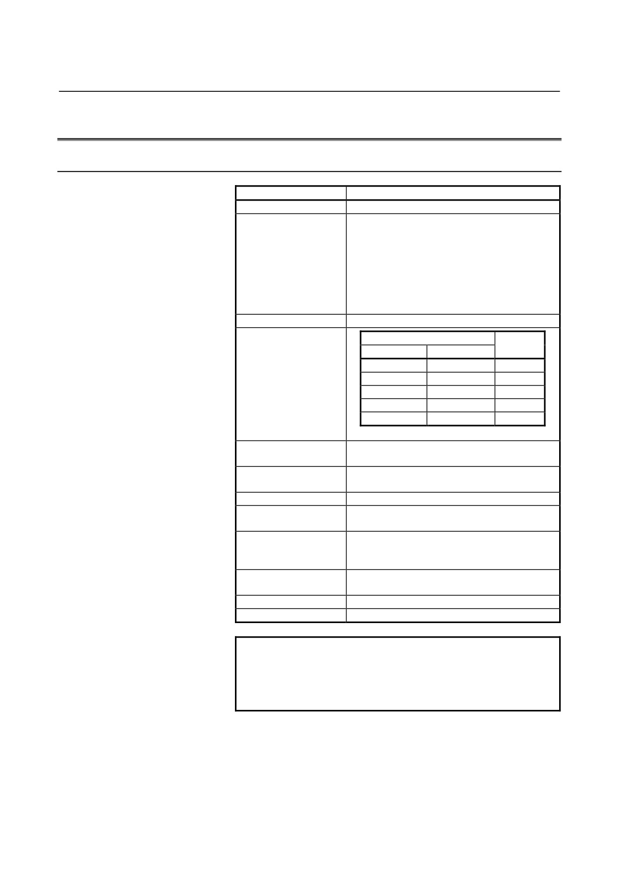
Item
Specifications
Number of input channel
4 channel/module
Analog input
• Voltage input
-10VDC to+10VDC(input resistance 4.7MΩ)
• Current input
-20mADC to+20mADC(input resistance 250Ω)
Caution) Which method to use, voltage input or
current input, can be selected by
connecting the corresponding input to the
terminal block.
Digital output
16 bit binary (complementary representation of "2".)
Input/output
Analog input
Digital
correspondence
Voltage input
Current input
output
+10V
-
+32000
+5V
+20mA
+16000
0
0
0
-5V
-20mA
-16000
-10V
-
-32000
Resolution
Voltage input: 0.3125mV
Current input: 1.25µA
Total precision
Voltage input: ±0.5%(For full scale)
Current input: ±1%(For full scale)
Conversionary time
Max.2ms (Note)
Maximum input
±15V, ±30mA
voltage/current
Isolation
Photocoupler isolated (between the input signal and
the base)
However, not isolated between input channels
Output connecting
Removable terminal block(20 terminals, M3.5
screw terminal)
Required input points
64 points
Name assigned to module
“AD04A” or “/8”
NOTE
Conversion time means that only in a module.
Actual response speed is determined by adding the
scanning time depending on each system to this
conversion time.
- 86 -
B-61813E/04
CONNECTION
6.ANALOG INPUT MODULE
6.2.2
Correspondence between Input Signals and Addresses in a
Module
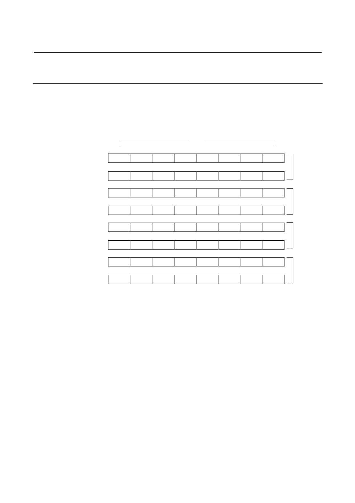
In the analog input module AAD04B, the 4-channel analog input
signals are cyclically A-D converted in order, and the converted digital
data are written in the following addresses. Therefore, in the PMC
program, it is possible at any time to know the values for the analog
input signals by referring to the following addresses.
Address
Bits
in module
7
6
5
4
3
2
1
0
0
D07-0
D06-0
D05-0
D04-0
D03-0
D02-0
D01-0
D00-0
Channel 0
1
D15-0
D14-0
D13-0
D12-0
D11-0
D10-0
D09-0
D08-0
2
D07-1
D06-1
D05-1
D04-1
D03-1
D02-1
D01-1
D00-1
Channel 1
3
D15-1
D14-1
D13-1
D12-1
D11-1
D10-1
D09-1
D08-1
4
D07-2
D06-2
D05-2
D04-2
D03-2
D02-2
D01-2
D00-2
Channel 2
5
D15-2
D14-2
D13-2
D12-2
D11-2
D10-2
D09-2
D08-2
6
D07-3
D06-3
D05-3
D04-3
D03-3
D02-3
D01-3
D00-3
Channel 3
7
D15-3
D14-3
D13-3
D12-3
D11-3
D10-3
D09-3
D08-3
D00-n and D15-n correspond to the weights of 20 and 215 respectively.
Here, D15-n corresponds to the sign bit in the complementary
representation of "2." (where n represents one of the channel numbers 0
to 3)
- 87 -
6.ANALOG INPUT MODULE
CONNECTION
B-61813E/04
NOTE
1 When addressing I/O modules, the beginning
address for this module should be assigned to an
even one. Moreover, when an A-D converted value is
referred to in a PMC program, make sure to read the
data in unit of a word (16 bits).
2 This module has a very high resolution. When
A/D-converted values are input to a system for
reference by the PMC program, they may disperse
largely depending on the system. If this is the case,
the dispersion of input values can be suppressed by
obtaining their moving average in the PMC program
or lowering the resolution by masking the
lowest-order bit if possible.
3 Note that on the PMC-N, -NA, and -QA (PMC for the
Series 15 and F-D Mate), the high-order one byte and
low-order one byte of a word (16 bits) are
interchanged with each other as described below.
Addresses for word-unit operation in the PMC-N, NA, and QA
Analog input module → PMC
Address in the
module
High-order byte
Low-order byte
Channel 0
0
D07-0 to D00-0
D15-0 to D08-0
Channel 1
+2
D07-1 to D00-1
D15-1 to D08-1
Channel 2
+4
D07-2 to D00-2
,D15-2 to D08-2
Channel 3
+6
D07-3 to D00-3
D15-3 to D08-3
- 88 -