FANUC I/O Unit–MODEL A CONNECTION AND MAINTENANCE MANUAL MARMGIOMA12801E REV. F (B-61813EN/06) - page 5
B-61813E/06
CONNECTION
7.ANALOG OUTPUT MODULE
7.2
14-BIT ANALOG OUTPUT MODULE (ADA02B)
7.2.1
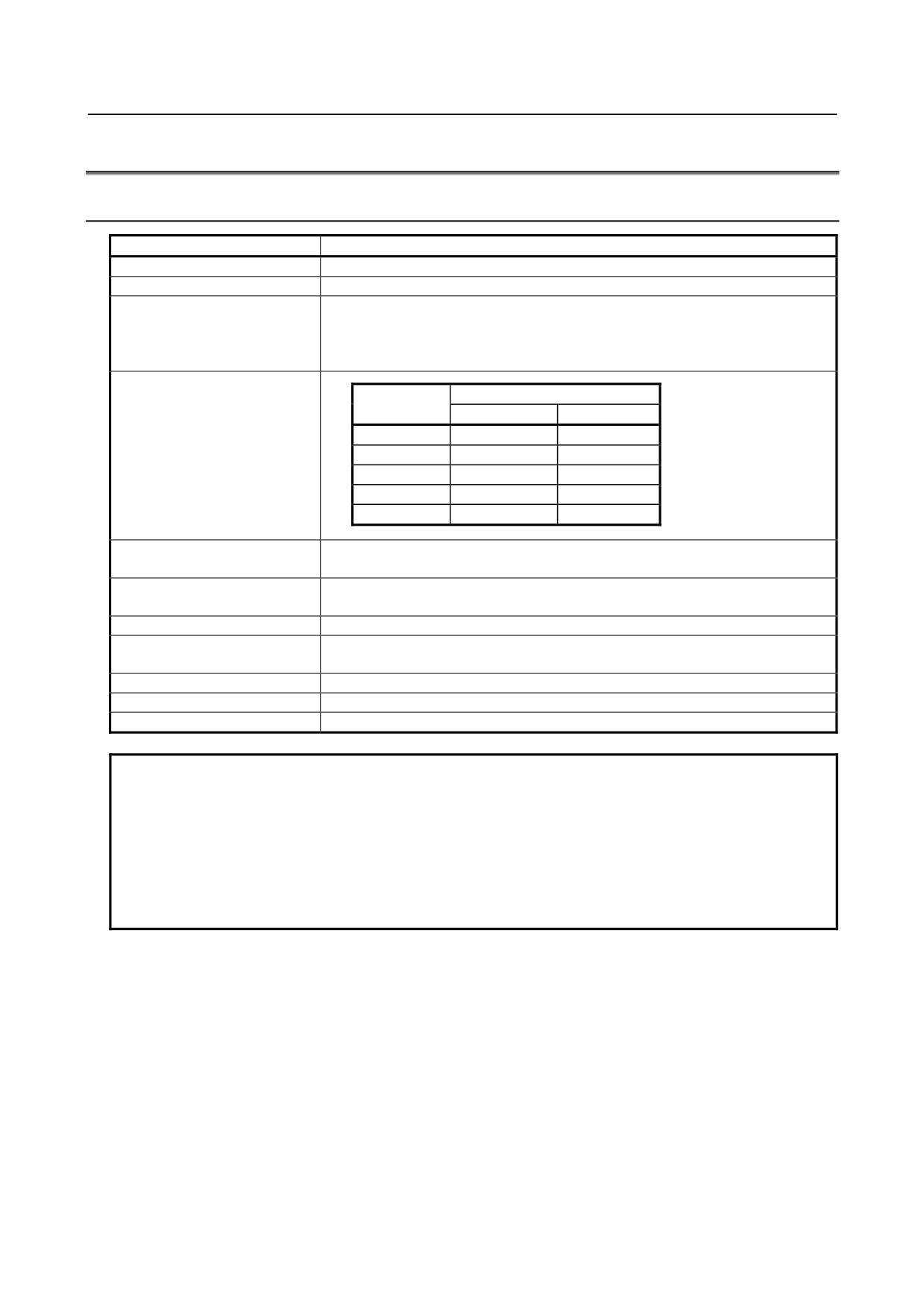
Specification
Item
Specification
Number of output channels
2 channels/module
Digital input
14-bit binary (2's complement representation)
Analog output
•Voltage output
-10 VDC to +10 VDC (external load resistance of 10 kΩ or higher) (Note 1)
•Current output
0 mADC to +20 mADC (external load resistance of 400Ω or lower)
Input/output correspondence
Analog output
Digital input
Voltage output
Current output
+8000
+10V
+20mA
+4000
+5V
+10mA
0
0
0
-4000
-5V
-
-8000
-10V
-
Resolution
Voltage output: 1.25 mV
Current output: 2.5 μA
Overall precision
Voltage output: ±0.5% (of the full scale)
Current output: ±1% (of the full scale)
Converting time
1 msec or shorter (Note 2)
Insulation
Photocoupler-based insulation between output signal and base, but no insulation
between output channels
External connection
Removable terminal block (20 terminals, M3.5 screw terminal)
Number of occupied output points
32 points
Name assigned to module
“DA02A” or “/4”
NOTE
1 Which method to use, voltage input or current input, can be selected by
connecting the corresponding input to the terminal block.
2 The converting time is that inside the module. The actual response time is added
the scan time that is determined by the system.
3 If this module is connected to any unit that requires a separate power supply, turn
on the I/O Unit-A before that unit. Turning on that unit before the I/O Unit-A may
lead to an accident dew to incorrect output or malfunction.
- 95 -
7.ANALOG OUTPUT MODULE
CONNECTION
B-61813E/06
7.2.2
Correspondence between Output Signals and Addresses in
the Module
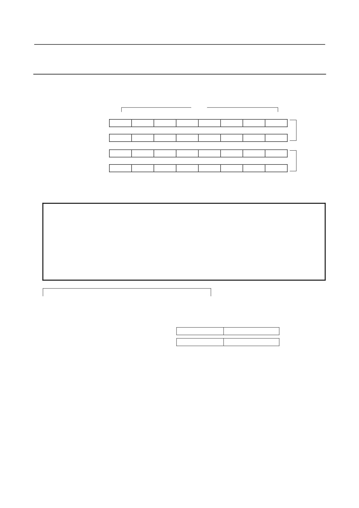
In the ADA02B analog output module, a 14-bit digital value is written to each of the following address to
output the desired voltage/current from its corresponding analog output.
Address
Bits
in module
7
6
5
4
3
2
1
0
0
D07-0
D06-0
D05-0
D04-0
D03-0
D02-0
D01-0
D00-0
Channel 0
1
-
-
D13-0
D12-0
D11-0
D10-0
D9-0
D8-0
2
D07-1
D06-1
D05-1
D04-1
D03-1
D02-1
D01-1
D00-1
Channel 1
3
-
-
D13-1
D12-1
D11-1
D10-1
D9-1
D8-1
D00-n (where n is 0 or 1) corresponds to a weight of 20, and D13-n to a weight of 213. However, D13-n
corresponds to the sign bit of a two's complement representation.
NOTE
1 I/O Link requires that the start address of each I/O module be even-numbered. To
write a value that is to be converted from digital to analog into a PMC program, be
sure to write it in words (16 bits).
2 I/O Link i does not care whether the start address of this module is even- or
odd-numbered.
3 Note that on the PMC-N, -NA, and -QA (PMC for the Series 15 (Series 15
preceding the i series) and F-D Mate), the high-order one byte and low-order one
byte of a word (16 bits) are interchanged with each other as described below.
Addresses for word-unit operation in the PMC-N, NA, and QA
PMC → 14-bit analog output module
Module in address
High-order byte
Low-order byte
Channel 0
0
D07-0 to D00-0
D13-0 to D08-0
Channel 1
+2
D07-1 to D00-1
D13-1 to D08-1
- 96 -
B-61813E/06
CONNECTION
7.ANALOG OUTPUT MODULE
7.2.3
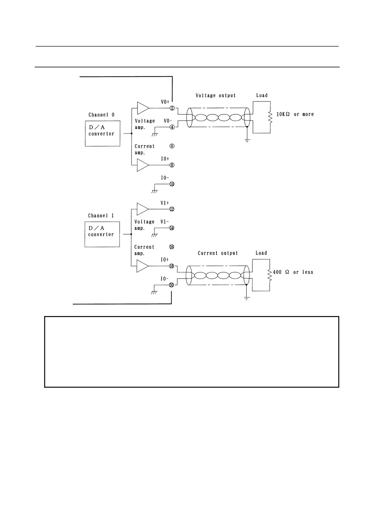
Connection between the Analog Output Module and Load
ADA02B
NOTE
1 Use a shielded 2-conductor twisted pair cable for the connection between the
analog output module and load.
2 Ground the shielding wire of the cable only at one point on the load side
(single-point grounding). However, both ends grounding or both ends opening
may be more effective depending on the environment where the unit is used.
Select one of the grounding types, whichever is appropriate, depending on what
the ambient noise is like.
- 97 -
8.HIGH-SPEED COUNTER MODULE CONNECTION
B-61813E/06
8 HIGH-SPEED COUNTER MODULE
8.1
OUTLINE OF HIGH-SPEED COUNTER MODULE
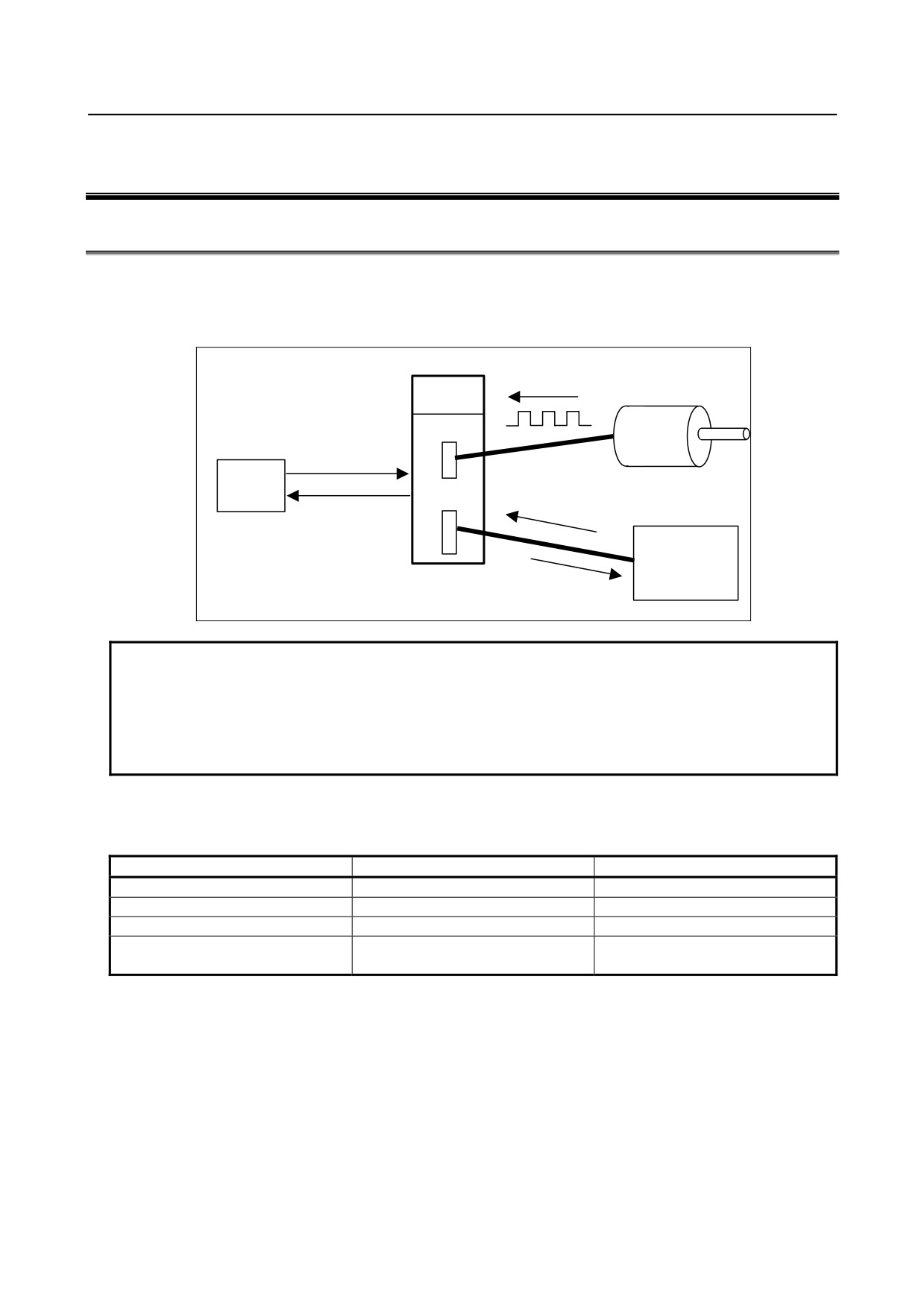
The high-speed counter module consists of a counter which counts the pulses sent from a pulse generator
such as a position detector in the machine tool and comparison registers for comparing preset values with
counter data. The module can read the counter data and output the results of comparison to the machine.
ACT01A
Pulse generator
JA9
Counter setting
CNC
C49
Counter control
Count value
Power
magnetics
High-speed counter module
cabinet
Comparison
result
NOTE
1 The FANUC manual pulse generator cannot be connected because it is not of line
driver output type.
2 The high-speed counter modules whose unit drawing number is A03B-0819-C053
or A03B-0807-C053 are dedicated to I/O Link. For I/O Link i, use the high-speed
counter module whose unit drawing number is A03B-0819-C064.
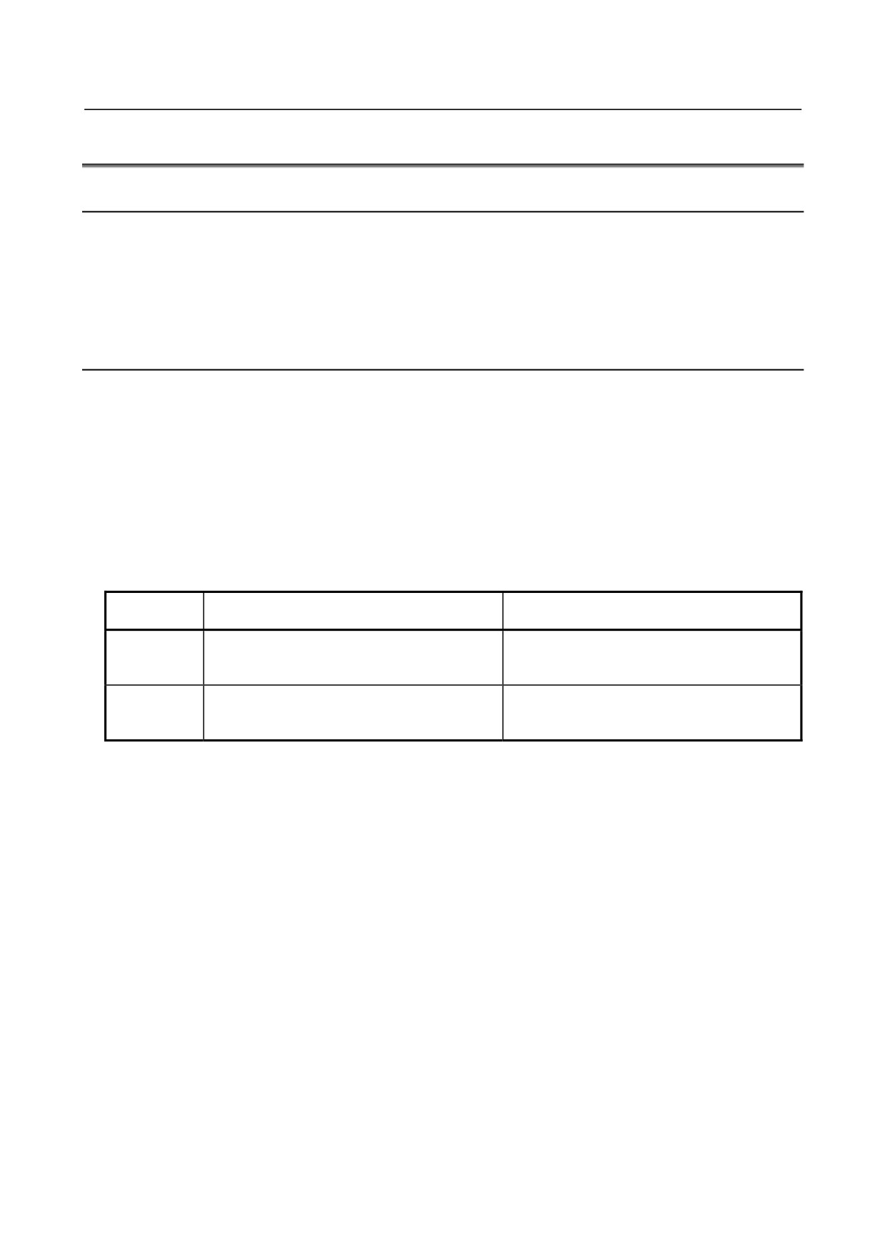
The high-speed counter module can run in two different modes, mode A and mode B. These two modes
differ in the way data is compared.
Mode A
Mode B
Number of comparison registers
3
16
Comparison output (PMC)
1bit
8bit
Comparison output (SSR)
1bit
8bit
Input 4 bytes
Input 8 bytes
PMC occupation area
Output 4 bytes
Output 4 bytes
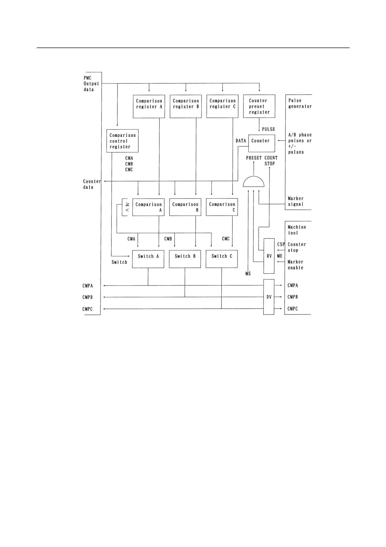
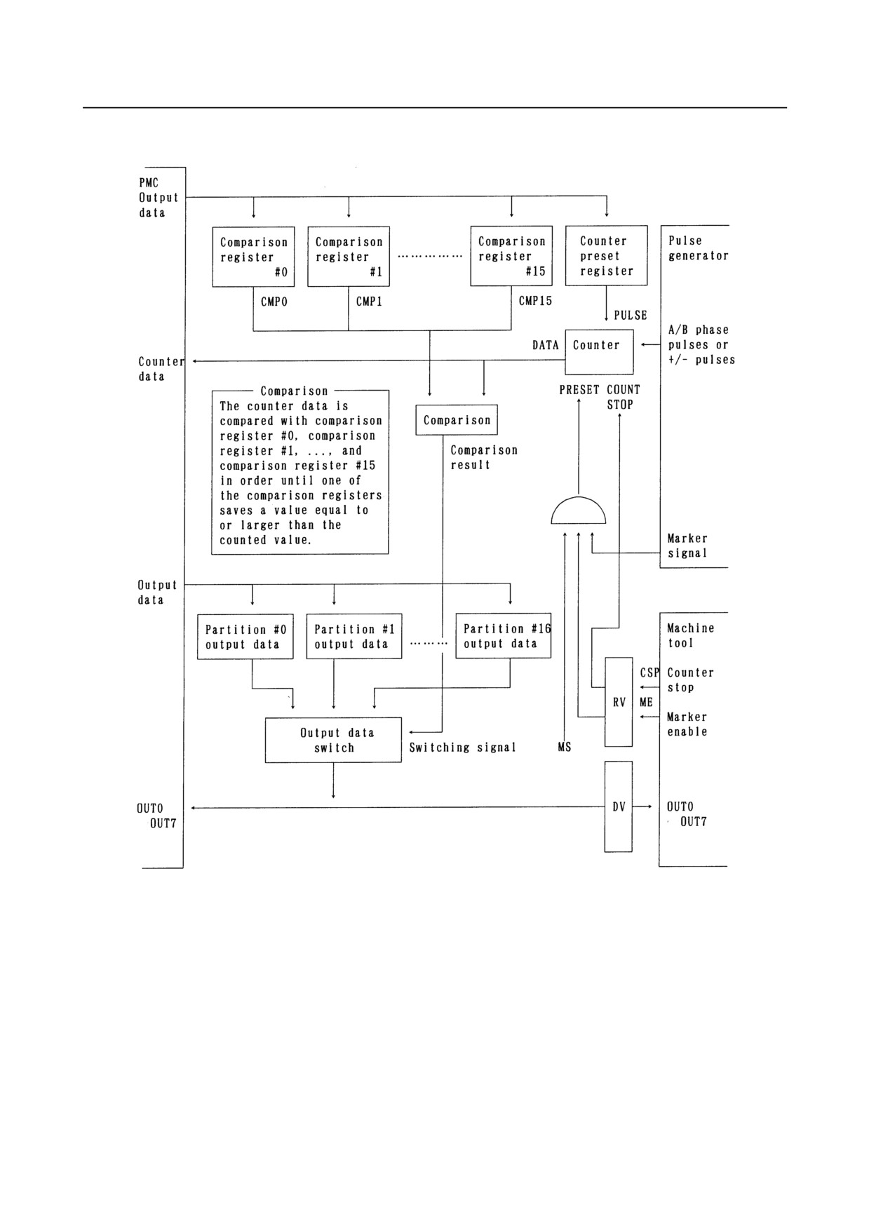
Shown below are configuration diagrams, briefing either mode.
- 98 -
B-61813E/06
CONNECTION 8.HIGH-SPEED COUNTER MODULE
A. Mode A
- 99 -
8.HIGH-SPEED COUNTER MODULE CONNECTION
B-61813E/06
B. Mode B
to
to
- 100 -
B-61813E/06
CONNECTION 8.HIGH-SPEED COUNTER MODULE
8.2
SPECIFICATIONS OF HIGH-SPEED COUNTER MODULE
8.2.1
Pulse Counter
(1) Binary up/down counter (1)
(2) Counter capacity
0 to 8,388,607
(3) Counter data
The pulse counter can preset data and read count data.
8.2.2
Comparison Function
(1) Mode A
A. Comparison register (23 bits)
Comparison registers A, B, and C are provided. The values to be compared are preset in the
comparison registers.
B. Comparison output
The results (CMPA, CMPB, and CMPC) of comparing the count data in the pulse counter with
the data set in the comparison registers are output.
C. Comparison output values
The comparison output values are set as listed in the table below. The values depend on the states
of CMA, CMB, and CMC, the comparison mode signals from the PMC.
Counter value
Counter value
≤ comparison register value
> comparison register value
CMA=0
CMPA=0
CMPA=1
CMB=0
CMPB=0
CMPB=1
CMC=0
CMPC=0
CMPC=1
CMA=1
CMPA=1
CMPA=0
CMB=1
CMPB=1
CMPB=0
CMC=1
CMPC=1
CMPC=0
(2) Mode B
A. Comparison register (23 bits)
There are 16 comparison registers #0,#1, ...,#15. The values to be compared are preset in the
comparison registers. The preset value in a comparison register having a larger register number
should be larger than that in a comparison register having a smaller register number, as follows:
Value in register #0 < value in register #1< ... < value in register #14 < value in register 15
B. Comparison output
The results (OUT0 to OUT7) of comparing the count data in the pulse counter with the data set in
the comparison registers are output.
C. Comparison output values
The count data in the pulse counter is compared with the values in the comparison registers in
sequential order from register 0 until the count data is equal to or less than the value in a
comparison register. This enables a partition to be made which includes the count data. Then the
output data for the partition (which is previously preset) is output. Eight output points (OUT0 to
OUT7) are provided.
If the count data is equal to the value in a comparison register, the data in the partition having the
same number as the register number is output.
- 101 -
8.HIGH-SPEED COUNTER MODULE CONNECTION
B-61813E/06
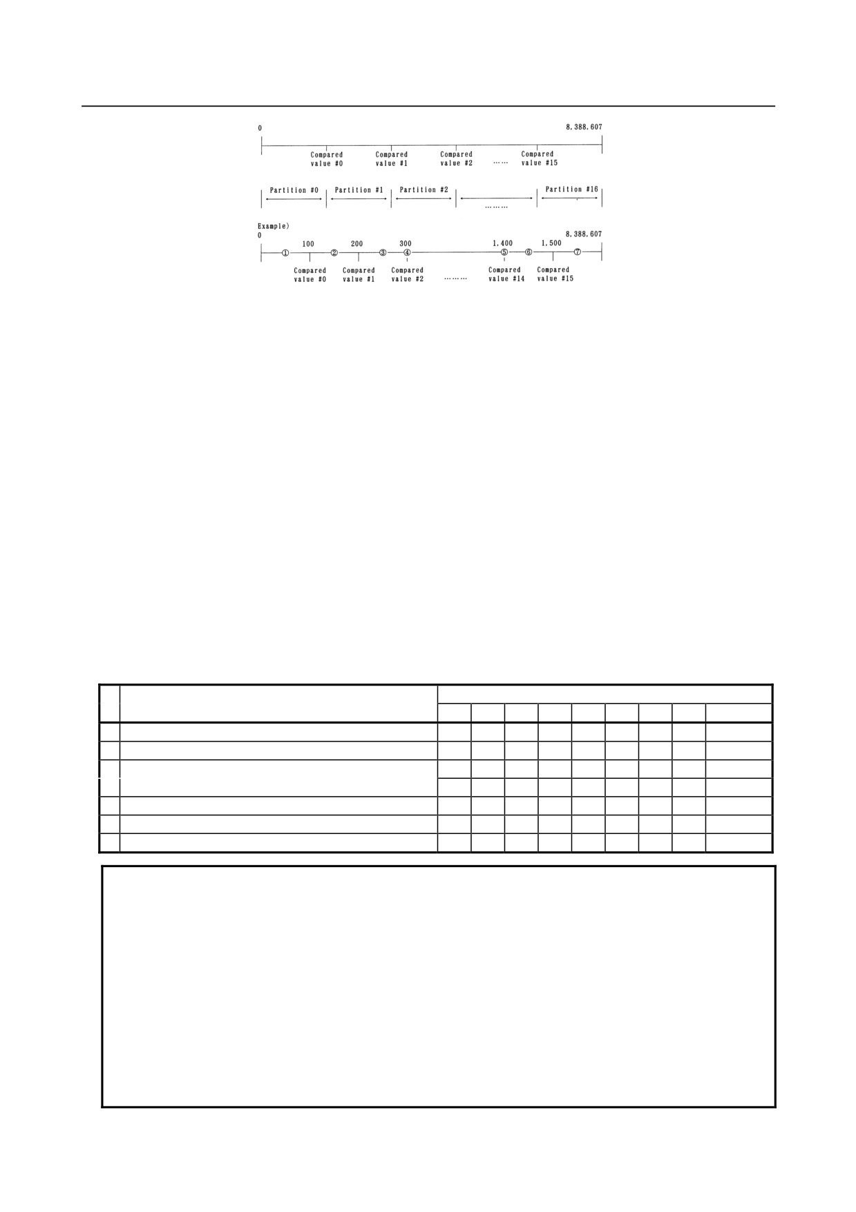
Assume that, when count data is in partition #n, the data to be output is set to respective values in
hexadecimal as listed below.
Output data from partition #0 = 0H
Output data from partition #1 = 1H
Output data from partition #2 = 2H
Output data from partition #3 = 3H
Output data from partition #4 = 4H
Output data from partition #5 = 5H
Output data from partition #6 = 6H
Output data from partition #7 = 7H
Output data from partition #8 = 8H
Output data from partition #9 = 9H
Output data from partition #10 = 10H
Output data from partition #11 = 11H
Output data from partition #12 = 12H
Output data from partition #13 = 13H
Output data from partition #14 = 20H
Output data from partition #15 = 21H
Output data from partition #16 = FFH
The output data is set as listed in the table below, depending on the counter values in c to i
above.
OUT
Partition
7
6
5
4
3
2
1
0
HEX value
①
0≤Counter value≤100
0
0
0
0
0
0
0
0
0h
②
100<Counter value≤200
0
0
0
0
0
0
0
1
1h
③
0
0
0
0
0
0
1
0
2h
200<Counter value≤300
④
0
0
0
0
0
0
1
0
2h
⑤
Comparison value in partition 14<Counter value≤1400
0
0
1
0
0
0
0
0
20h
⑥
1400<Counter value≤1500
0
0
1
0
0
0
0
1
21h
⑦
1500<Counter value≤8,388,607
1
1
1
1
1
1
1
1
FFh
NOTE
1 Preset an increasingly larger value in each of the compare registers (#0, #1, ...,
#15) as the register number becomes larger.
Unless this condition is satisfied, it is likely that no normal compensation may take
place, leading to an abnormal compare output.
2 When using 15 or less partitions, it is not necessary to set all of 16 partitions.
Example)
Count value
0 to 100
Partition #0
101 to 1000 Partition #1
1001 to
Partition #2
In this case, partition #3 and later do not need to be set.
- 102 -
B-61813E/06
CONNECTION 8.HIGH-SPEED COUNTER MODULE
8.2.3
Pulse Interface
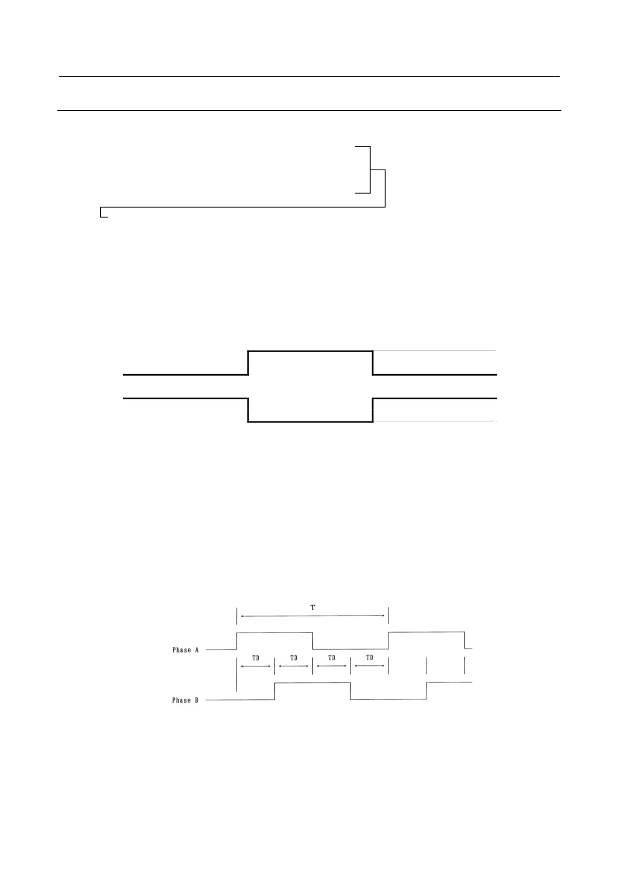
The following three types of pulses are entered in the high-speed counter module.
A. Phase A/B pulses: The phase difference between
these detection pulses is 90°
B.
+/- pulses: These detection pulses are separated
in the positive and negative directions.
Select either type of the detection pulse.
C. Marker signal: Used to preset data in the pulse counter.
(1) Phase A/B pulse interface
The phase A/B pulses are selected when the PSEL signal is open.
A. Interface IC
The signal of the pulse generator connected to the high-speed counter module is equivalent to that
of the line driver SN75113. It also equivalent to that of the AM26LS31. The signals involved are
the equilibrium transmission signals shown below.
Voh
PA
Vol
Voh
*PA
Vol
(The PB and MKS signals are the same, respectively, as PA and *PB. The *MKS signal is the
same as *PA.)
For the receiver of this module, the voltage rating is 0 to 5 V, Voh = 2.0 V or higher, and Vol =
0.8 V or lower. The pulse generator to be connected to the module must have a driver that meets
these voltage requirements.
If you want to use a commercial rotary encoder as the pulse generator, select "line driver type
output" that meets the above voltage requirements. The other output types
(such as
open-collector output or voltage output type) cannot be used.
B. Maximum frequency =125KHz
Tmin.
=8μS
(minimum period)
TDmin.
=1.2μS (minimum time between edges)
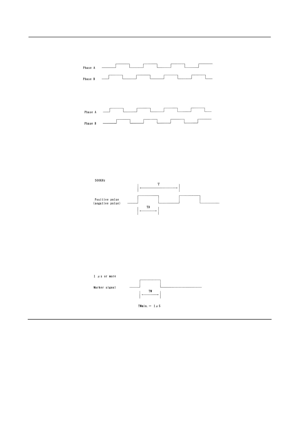
C. Count and direction
A counter multiplied by four compared to phase A and B pulses is provided. It counts positive
when phase A advances before phase B and it counts negative when phase B advances before
phase A.
- 103 -
8.HIGH-SPEED COUNTER MODULE CONNECTION
B-61813E/06
Positive count
Advance of phase A before phase B
Negative count
Advance of phase B before phase A
(2) Positive/negative pulse interface
Positive and negative pulses are selected when the PSEL signal is connected to 0 VDC.
A. Interface IC
See Paragraph A, "Interface IC", in Item (1), "Phase A/B pulse interface".
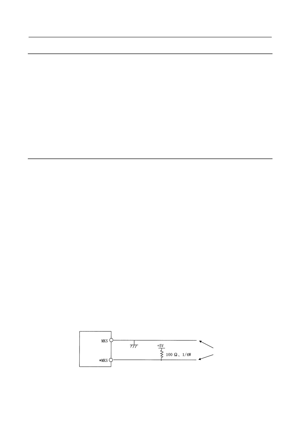
B. Maximum frequency
Tmin.
= 2μS
(minimum period)
TDmin. = 0.5μS
(minimum pulse width)
(3) Marker signal
A. Interface IC
Use differential drivers (SN75113 or equivalent) at the output ports of the pulse generator.
B. Minimum pulse width
8.2.4
External Contact Input
The pulse counter module uses insulating receivers (having a voltage rating of 24 VDC) at the input ports.
The following two types of signal inputs are provided.
(1) Marker enable signal input (ME)
The contact of the marker enable signal is closed to make the marker signal valid.
This enables data to be preset in the counter.
(2) Count stop signal input (CSP)
The contact of the count stop signal is closed to stop the count operation.
- 104 -
B-61813E/06
CONNECTION 8.HIGH-SPEED COUNTER MODULE
8.2.5
External Contact Output
Solid state relays (SSR) are used for the contacts.
(1) Mode A
The comparison mode signal outputs A, B, C (CMPA, CMPB, and CMPC) are provided in mode A.
These outputs indicate the results of comparing the comparison registers A, B, and C with the pulse
counter. The comparison output values are determined depending on whether the control mode signals
(CMA, CMB, and CMC) from the PMC are set to 1 or 0.
(2) Mode B
The results of comparing comparison register #0, comparison register #1, ..., comparison register #15
with the pulse counter are provided in mode B. The comparison output indicates the values in the
output data registers for the partitions in which the count data is located. Eight output points are
provided. (See Section 8.2.2 (2))
8.2.6
Marker Processing
(1)
Mode A
A. Synchronization with marker
The counter value is set to the data in the counter preset register at the rising edge of the first
marker signal with the MS signal output from the PMC set to 1 and the contact of the marker
enable signal input (ME) from the machine closed.
B. Marker hold
The MH signal is set to 1 at the rising edge of the first marker signal with the MS signal output
from the PMC set to 1 and the contact of the marker enable signal input (ME) from the machine
closed. The MH signal is reset when the marker hold reset (MHR), an output signal from the
PMC, is set to 1 or the MS signal output from the PMC is set to 0.
(2)
Mode B
A. Synchronization with marker
When the MS signal output from the PMC is 1 and the contact of the marker enable (ME) signal
input from the machine is closed, the counter is set to the data in the counter preset register at the
rising edge of the first marker signal.
B. Maker hold
When the MS signal output from the PMC is 1 and the contact of the marker enable (ME) signal
input from the machine is closed, the MH signal is set to 1 at the rising edge of the marker signal.
The MH signal is reset when the MS signal output from the PMC is set to 0.
(3)
Pin treatment when no marker signal is used
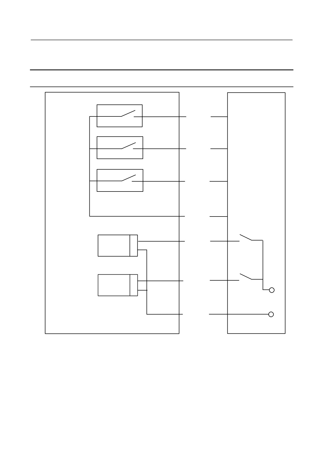
If you use (that is, preset) no marker signal, treat the corresponding pin as shown below. Otherwise, a
broken-wire alarm will be raised. The counter keeps running even after a broken-wire alarm is raised,
though.
Counter module
Cable
If the treatment shown above cannot prevent a broken-wire alarm from being raised, make sure that the
GND terminal of the pulse generator is connected to the LGND (0V) pin of the JA9 connector.
- 105 -
8.HIGH-SPEED COUNTER MODULE CONNECTION
B-61813E/06
8.2.7
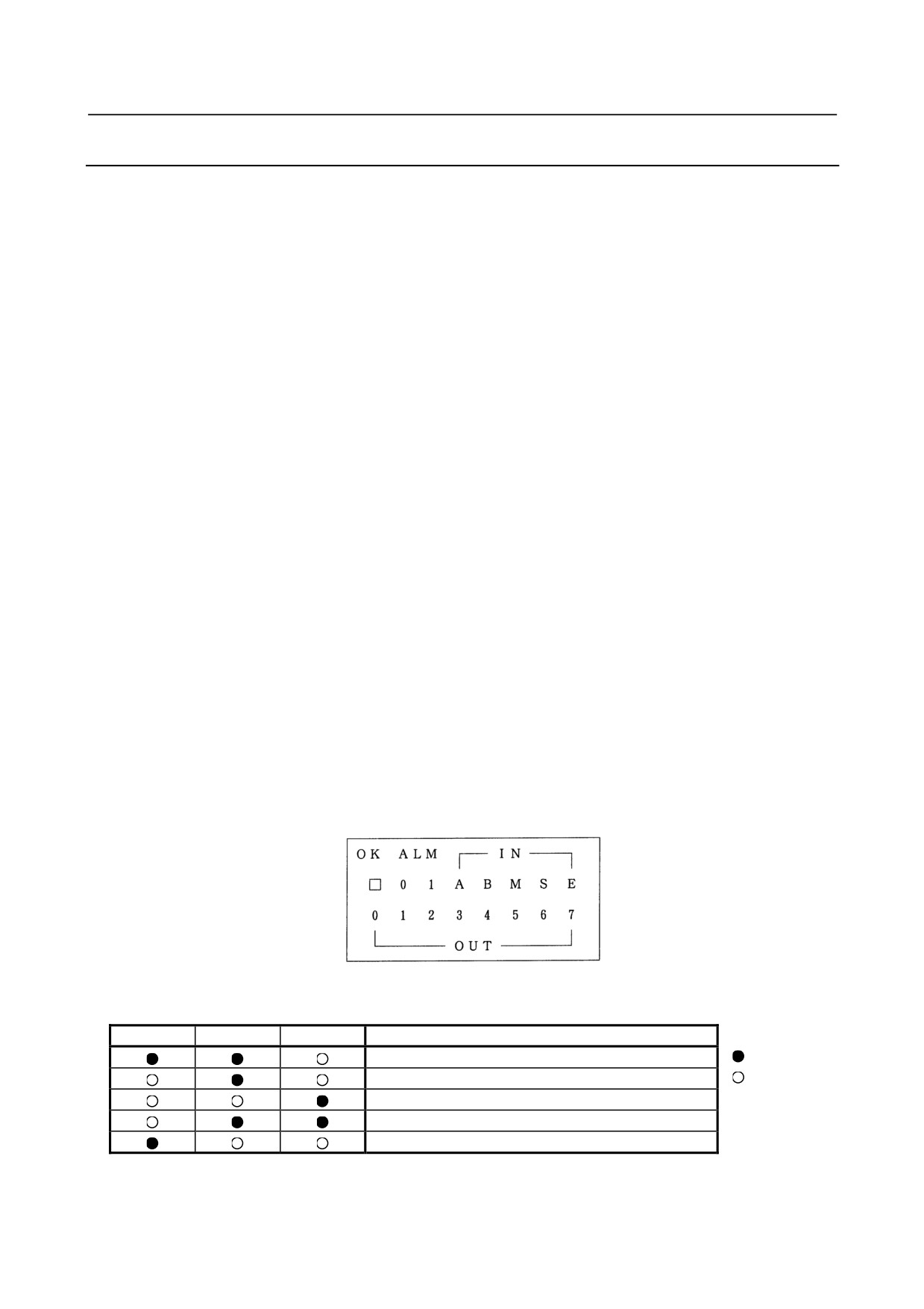
LED indicators
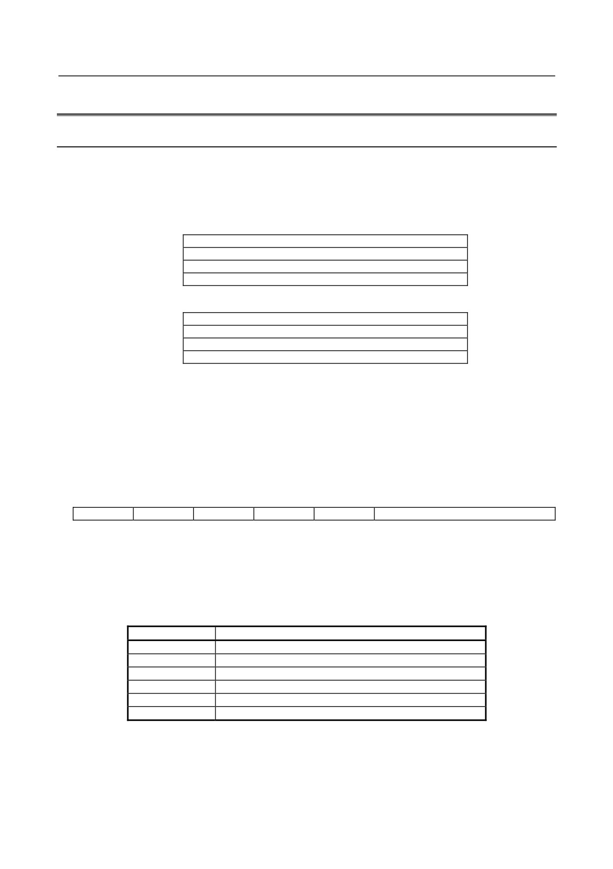
The high-speed counter module has the following indicators.
(1)
OK indicator
See below Table.
(2)
ALM0 and ALM1 indicators
See below Table.
(3)
Phase A and B pulses (positive and negative pulses) input signal indicators (A and B)
The phase A pulse input signal indicator is on when the phase A pulse input is active.
The phase B pulse input signal indicator is on when the phase B pulse input is active.
If the pulse remains "1" (high) only for a short time and has a long period, it is difficult to recognize
a blinking LED.
(4)
Marker signal indicator (M)
The marker signal indicator is on while the marker signal (MP) from the pulse generator is active.
(5)
Count stop signal indicator (S)
The count stop signal indicator is on when the contact of the count stop signal input sent from the
machine is closed.
(6)
Marker enable signal indicator (E)
The marker enable signal indicator is on when the contact of the marker enable signal input sent from
the machine is closed.
(7)
Comparison result output indicators (OUT0, OUT1, OUT2, OUT3, OUT4, OUT5, OUT6, and OUT7)
A. Mode A
The indicators OUT0, OUT1, and OUT2 correspond to the signals CMPA, CMPB, and CMPC.
OUT1 goes on when CMPA goes on, OUT2 goes on when CMPB goes on, and OUT3 goes on
when CMPC goes on.
B. Mode B
The indicators OUT0-OUT7 go on corresponding to when the output data OUT0-OUT7 resulting
from the comparisons between the count data and comparison resisters are set to 1.
LED indicator panel
OK
ALM0
ALM1
Explanation of alarm
Disconnection alarm
: On
Self-diagnosis alarm, RAM error
: Off
Self-diagnosis alarm, ROM error
Watch dog alarm
Normal operation
The state of the OK, ALM0, or ALM1 is not held.
- 106 -
B-61813E/06
CONNECTION 8.HIGH-SPEED COUNTER MODULE
8.3
PMC INTERFACE
8.3.1
Mode A
(1) PMC I/O area
In mode A, four input bytes and four output bytes are used as the I/O area. The bytes in the I/O area
have the following names. The input and output directions are specified on the basis of the PMC. The
operation mode is set to mode A at power-on.
(a) Output data (sent from PMC to high-speed counter module)
0
CTRL (control)
+1
DTOH (higher 8-bit data)
+2
DTOM (middle 8-bit data)
+3
DTOL (lower 8-bit data)
(b) Input data (entered from high-speed counter module to PMC)
0
CNTS (counter H and status)
+1
CNTM (middle 8 bits of counter)
+2
CNTL (lower 8 bits of counter)
+3
STTS (status)
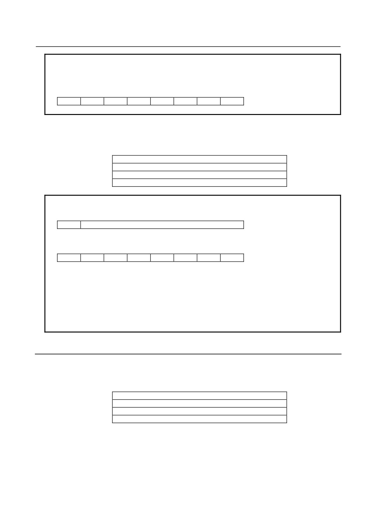
(2) PMC outputs (entered from PMC to high-speed counter module)
The PMC outputs are separated into control output CTRL and data outputs DTOH, DTOM, and DTOL.
As with normal DOs, the control outputs of bit 3 to bit 7 are controlled independently. The control
outputs of bit0 to bit2 constitute the SELECT indicating the target data specified by DTOH, DTOM,
and DTOL.
(a) Control output
CTRL
7
6
5
4
3
2
1
0
MHR
MS
CE
PRS
SELECT
PRS Preset
CE Count enable
MS Marker synchronization
MHR Marker hold reset
(b) Details of DTOH, DTOM, and DTOL
The SELECT bits indicate the target data.
SELECT
0
CCTR (comparison control)
1
Counter preset data
2
Comparison register A
3
Comparison register B
4
Comparison register C
7
Change to mode B
- 107 -
8.HIGH-SPEED COUNTER MODULE CONNECTION
B-61813E/06
NOTE
1 Change to mode B: See Subsection 8.3.2, "Mode B".
2 Detail of CCTR
DTOH
7
6
5
4
3
2
1
0
CMC
CMB
CMA
The DTOM and DTOL are ignored.
(3) PMC inputs (entered from high-speed counter module to PMC)
The inputs to the PMC include the status and counter data. The data is shown below.
0
CNTS (counter H and status)
+1
CNTM (middle 8 bits of counter)
+2
CNTL (lower 8 bits of counter)
+3
STTS (status)
NOTE
1 Details of CNTS
7
6
5
4
3
2
1
0
TRA
Counter H (most significant 7 bits)
TRA : Transfer A
2 Details of STTS
7
6
5
4
3
2
1
0
TRB
ALM
CSP
ME
MH
CMPC
CMPB
CMPA
CMPA
: Comparison output A
CMPB
: Comparison output B
CMPC
: Comparison output C
MH : Marker hold
ME : Marker enable
CSP : Count stop
ALM : Alarm (disconnection or watch dog alarm)
TRB : Transfer B
8.3.2
Mode B
Change to mode B
The operation mode is set to mode A at power-on. The following data is output to the counter module and
the mode changes from A to B. The mode cannot change from B to A.
0
CTRL
:
0FH (SELECT = 7, PRS = 1)
+1
DTOH
:
01H
+2
DTOM
:
00H
+3
DTOL
:
00H
(1) PMC I/O area
In mode B, eight input bytes and four output bytes are used as the I/O area. The bytes in the I/O area
have the following names. The input and output directions are specified on the basis of the PMC.
- 108 -
B-61813E/06
CONNECTION 8.HIGH-SPEED COUNTER MODULE
(a) Output data (sent from PMC to high-speed counter module)
0
CTRL (control)
+1
DTOH (higher 8-bit data)
+2
DTOM (middle 8-bit data)
+3
DTOL (lower 8-bit data)
(b) Input data (entered from high-speed counter module to PMC)
0
CNTS (counter H and status)
+1
CNTM (middle 8 bits of counter)
+2
CNTL (lower 8 bits of counter)
+3
STTS (status)
+4
OUTD
+5
MODD
+6
Unused
+7
Unused
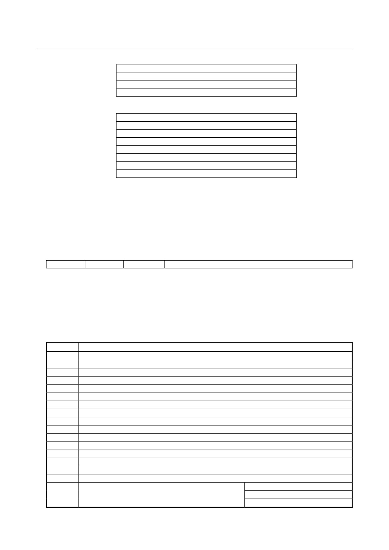
(2) PMC outputs (outputs from PMC)
The PMC outputs are separated into control output (CTRL) and data outputs (DTOH, DTOM, and
DTOL). As with normal DOs, the control outputs of bit 5 to bit 7 are controlled independently. The
control outputs of bit 0 to bit 4 constitute SELECT indicating the target data specified by DTOH,
DTOM, and DTOL.
(a) Control outputs
CTRL
7
6
5
4
3
2
1
0
MS
CE
PRS
SELECT
PRS Preset
CE Count enable
MS Marker synchronization
(b) Details of DTOH, DTOM, and DTOL
Enter the comparison value and preset value (24 bits) to the DTOH, DTOM, and DTOL.
Enter a comparison result (8 bits) output for each partition, respectively, to the DTOH, DTOM,
and DTOL.
SELECT
Target data
0
Comparison data : Specify a comparison value (24 bits) for partition #0.
1
Comparison data : Specify a comparison value (24 bits) for partition #1.
2
Comparison data : Specify a comparison value (24 bits) for partition #2.
3
Comparison data : Specify a comparison value (24 bits) for partition #3.
4
Comparison data : Specify a comparison value (24 bits) for partition #4.
5
Comparison data : Specify a comparison value (24 bits) for partition #5.
6
Comparison data : Specify a comparison value (24 bits) for partition #6.
7
Comparison data : Specify a comparison value (24 bits) for partition #7.
8
Comparison data : Specify a comparison value (24 bits) for partition #8.
9
Comparison data : Specify a comparison value (24 bits) for partition #9.
10
Comparison data : Specify a comparison value (24 bits) for partition #10.
11
Comparison data : Specify a comparison value (24 bits) for partition #11.
12
Comparison data : Specify a comparison value (24 bits) for partition #12.
13
Comparison data : Specify a comparison value (24 bits) for partition #13.
14
Comparison data : Specify a comparison value (24 bits) for partition #14.
15
Comparison data : Specify a comparison value (24 bits) for partition #15.
16
Comparison output data (8 bits) for partition #0 to #2
Partition #0: DTOH
Partition #1: DTOM
Partition #2: DTOL
- 109 -
8.HIGH-SPEED COUNTER MODULE CONNECTION
B-61813E/06
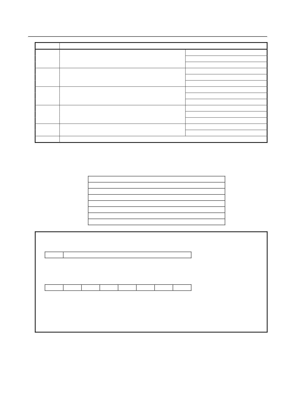
SELECT
Target data
17
Comparison output data (8 bits) for partition #3 to #5
Partition #3: DTOH
Partition #4: DTOM
Partition #5: DTOL
18
Comparison output data (8 bits) for partition #6 to #8
Partition #6: DTOH
Partition #7: DTOM
Partition #8: DTOL
19
Comparison output data (8 bits) for partition #9 to #11
Partition #9: DTOH
Partition #10: DTOM
Partition #11: DTOL
20
Comparison output data (8 bits) for partition #12 to #14
Partition #12: DTOH
Partition #13: DTOM
Partition #14: DTOL
21
Comparison output data (8 bits) for partition #15 and #16
Partition #15: DTOH
Partition #16: DTOM
22
Counter preset data (24 bits)
(The numbers of DTOH, DTOM, and DTOL indicate the output data for the partitions specified by the
numbers.)
(c) PMC inputs (inputs to PMC)
The inputs to the PMC include the status and counter data. The data is shown below.
0
CNTS (counter H and status)
+1
CNTM (middle 8 bits of counter)
+2
CNTL (lower 8 bits of counter)
+3
STTS (status)
+4
OUTD
+5
MODD
+6
Not used
+7
Not used
NOTE
1 Detail of CNTS
7
6
5
4
3
2
1
0
TRA
Counter H (most significant 7 bits)
TRA : Transfer A
2 Detail of STTS
7
6
5
4
3
2
1
0
TRB
ALM
CSP
ME
MH
MH : Marker hold
ME : Marker enable
CSP : Count stop
ALM : Alarm (disconnection or watch dog alarm)
TRB : Transfer B
- 110 -
B-61813E/06
CONNECTION 8.HIGH-SPEED COUNTER MODULE
NOTE
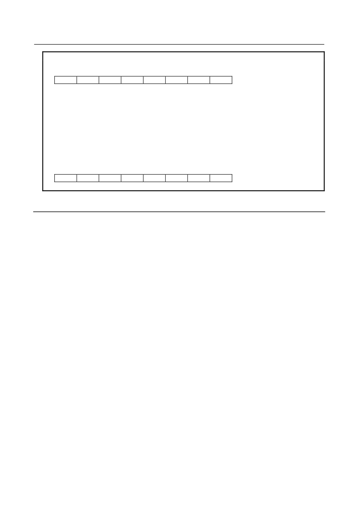
3 Detail of OUTD
7
6
5
4
3
2
1
0
OUT7
OUT6
OUT5
OUT4
OUT3
OUT2
OUT1
OUT0
OUT0
: Bit 0 of comparison output
OUT1
: Bit 1 of comparison output
OUT2
: Bit 2 of comparison output
OUT3
: Bit 3 of comparison output
OUT4
: Bit 4 of comparison output
OUT5
: Bit 5 of comparison output
OUT6
: Bit 6 of comparison output
OUT7
: Bit 7 of comparison output
4 Detail of MODD
7
6
5
4
3
2
1
0
MOD0
MOD0 : Set to 1 after the mode changes to B.
8.3.3
Details of PMC Interface Signals
(1)
PMC inputs (inputs from PMC)
(a)
TRA and TRB
The counter data is valid when TRA is equal to TRB and invalid when TRA is not equal to TRB.
(b)
CMPA, CMPB, and CMPC (comparison output signals A, B, and C, only in mode A)
The CMPA, CMPB, and CMPC signals are output signals resulting from the comparison
between the comparison registers A, B, and C and the counter data, respectively. The output
levels of CMPA, CMPB, and CMPC are determined by the comparison mode signals CMA,
CMB, and CMC.
When CMA, CMB, and CMC are 0, and the counter data is larger than the values in comparison
registers A, B, and C, CMPA, CMPB, and CMPC are set to 1.
When CMA, CMB, and CMC are 1, and the counter data is equal to or less than the values in
comparison registers A, B, and C, CMPA, CMPB, and CMPC are set to 1.
(c)
OUT0 to OUT7 (comparison output signal 0 to comparison output signal 7, only in mode B)
OUT0 - OUT7 correspond to bit 0 to bit 7 in the comparison result output of a single byte.
(d)
MH (marker hold signal)
The marker hold signal MH is set to 1 at the rising edge of the marker signal when the marker
enable signal is 1. The marker hold signal is reset when MHR=1 or MS=0. (In mode B, the
marker hold signal MH is reset only when MS=0.)
(e)
ME (marker enable signal)
The marker enable signal ME enables the marker signal as follows:
ME=1: Marker signal enabled
ME=0: Marker signal disabled
(f)
CSP (count stop signal)
The counter stops counting when the contact for the external input signal CSP is closed.
(g)
ALM (alarm signal)
The alarm signal ALM is set to 1 if the signal line for the count pulse or the marker signal is
disconnected or short-circuited.
ALM is also set to 1 if a watchdog alarm occurs due to a failure in the CPU in the module.
- 111 -
8.HIGH-SPEED COUNTER MODULE CONNECTION
B-61813E/06
(2)
PMC outputs (outputs from PMC)
(a)
SELECT (selection signal)
The SELECT signal selects the register in which data will be set. That is, the signal specifies the
register for presetting data. The SELECT signal should be set when or before the PRS signal is
reversed.
(b)
PRS (preset signal)
The PRS signal presets data in registers. If data is set in DTOH, DTOM, and DTOL and then PRS
is reversed, the data is set in the register specified by SELECT. Reversing the PRS signal means
that PRS changes from level 0 to level 1 or vise versa.
DTOH, DTOM, DTOL, and SELECT should not be changed within two scans after the PRS is
reversed. Also, the PRS must not reversed again within this period.
When SELECT=1, data is set in both the counter preset register and the counter.
Data is set by setting the first PRS to 1 after power-on or after the mode changes to B.
(c)
CE (count enable signal)
The CE signal determines whether the counter counts. When the CE is set to 1 and the external
input signal CSP closes the contact, the counter retains its value, instead of counting. When CE =
1 and the CSP external input contact is open, the counter counts input pulses. Presetting the
counter requires maintaining CE = 0.
(d)
MS (marker synchronization signal)
The MS signal determines whether marker synchronization is provided. When the MS is 1 and
the contact of external input signal ME is closed, the counter is preset to the value in the counter
preset register at the rising edge of the first marker signal.
For mode A, after presetting:
<1> Set MS bit (0 → 1) again, or
<2> Reset MHR bit (1 → 0).
When either of the above conditions is satisfied, marker synchronization is established again.
(Note that item <2> is unusable for mode B.)
(e)
MHR (marker hold reset signal, only in mode A)
The MHR signal resets the marker hold (MH) signal which is output to the PMC. The MHR is
set to 1 to reset the marker hold signal.
(f)
CMA, CMB, and CMC (comparison mode signals A, B, and C, only in mode A)
The CMA, CMB, and CMC signals specify the levels of the comparison outputs A, B, and C
(CMPA, CMPB, and CMPC), respectively.
When CMA, CMB, and CMC are 0, and the value of the counter is larger than the values in
comparison registers A, B, and C, CMPA, CMPB, and CMPC are set to 0.
When CMA, CMB, and CMC are 1, and the value of the counter is equal to or less than the values
in comparison registers A, B, and C, CMPA, CMPB, and CMPC are set to 1.
- 112 -
B-61813E/06
CONNECTION 8.HIGH-SPEED COUNTER MODULE
8.4
TOTAL CONNECTION OF HIGH-SPEED COUNTER
MODULE
8.4.1
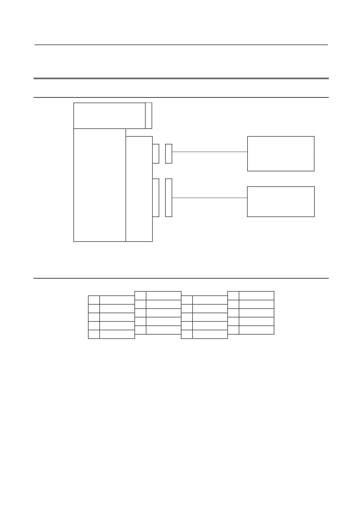
Connection Diagram
HONDA TSUSHIN (PCR-E20FA)
JA9
Detection pulse generator
C49
Machine (power magnetics
HIROSE ELECTRIC
cabinet)
(HIF-3BA-20D-2.54R)
A63L-0001-0472#S20
High-speed counter module
8.4.2
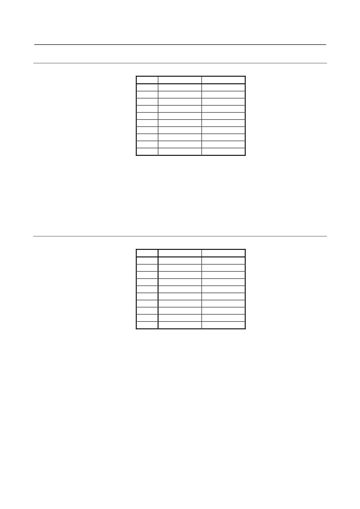
Connector Signal List
JA9
10
20
+5V
9
+5V
19
8
PSEL
18
+5V
7
LGND
17
6
*MKS
16
LGND
5
MKS
18
4
*PBS
14
LGND
3
PBS
13
2
*PAS
12
LGND
1
PAS
11
PAS Phase A pulse input signal (Negative pulse input signal) (positive)
*PAS Phase A pulse input signal (Negative pulse input signal) (negative)
PBS Phase B pulse input signal (Positive pulse input signal) (positive)
*PBS Phase B pulse input signal (Positive pulse input signal) (negative)
MKS Marker signal (positive)
*MKS Marker signal (negative)
PSEL Pulse select signal
+5V 5V (output from this module)
LGND 0V
- 113 -
8.HIGH-SPEED COUNTER MODULE CONNECTION
B-61813E/06
8.4.2.1 C49 signal (for mode A)
C49
A
B
01
ME
02
CSP
03
COM1
04
05
06
CMP A
07
CMP B
08
CMP C
09
10
COM2
ME Marker enable signal input
CSP Counter stop signal input
CMP A Comparison result output
CMP B Comparison result output
CMP C Comparison result output
COM1 Common signal for ME and CSP
COM2 Common signal for comparison result output CMP A to comparison result output CMP C
8.4.2.2 C49 signal (for mode B)
C49
A
B
01
ME
02
CSP
03
COM1
04
05
06
OUT0
OUT4
07
OUT1
OUT5
08
OUT2
OUT6
09
OUT3
OUT7
10
COM2
COM3
ME Marker enable signal input
CSP Counter stop signal input
OUT0 Comparison result output
OUT1 Comparison result output
OUT2 Comparison result output
OUT3 Comparison result output
OUT4 Comparison result output
OUT5 Comparison result output
OUT6 Comparison result output
OUT7 Comparison result output
COM1 Common signal for ME and CSP
COM2 Common signal for comparison result output 0 to comparison result output 3
COM3 Common signal for comparison result output 4 to comparison result output 7
- 114 -
B-61813E/06
CONNECTION 8.HIGH-SPEED COUNTER MODULE
8.5
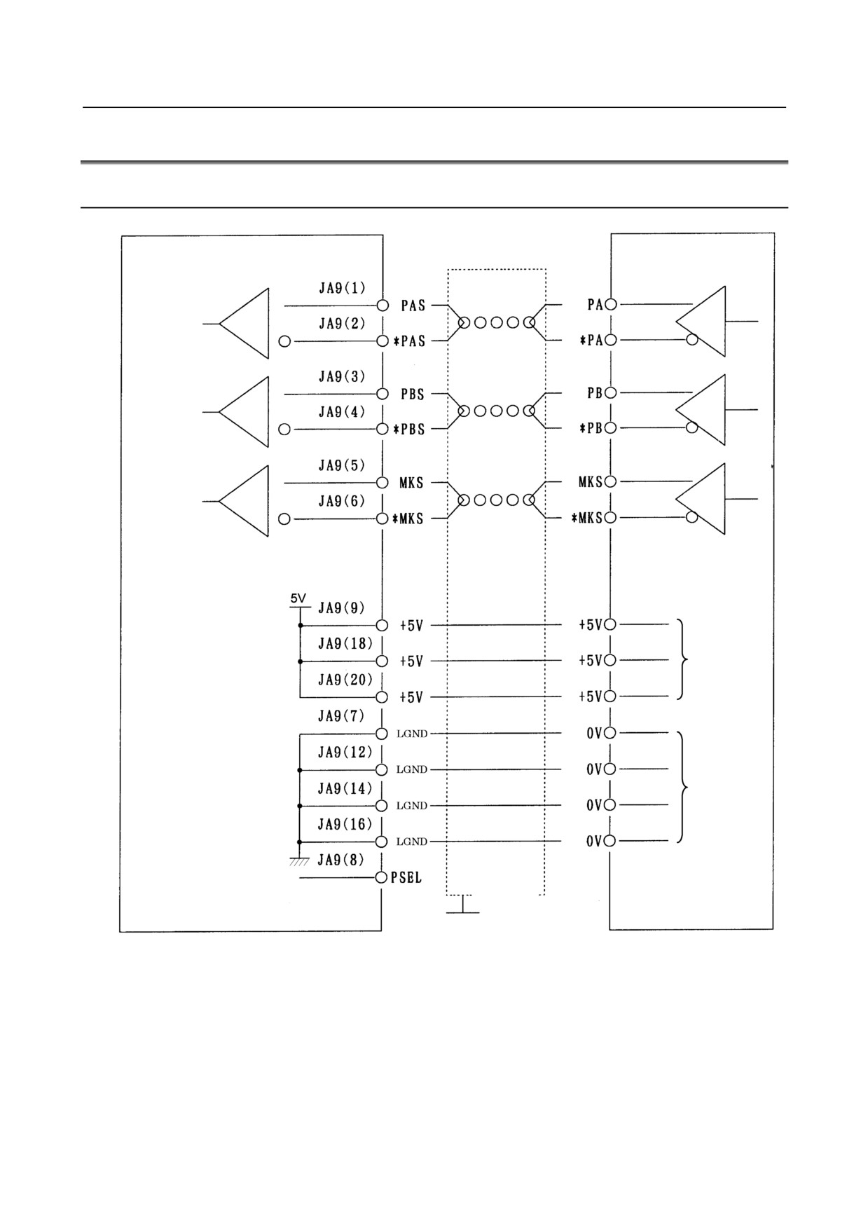
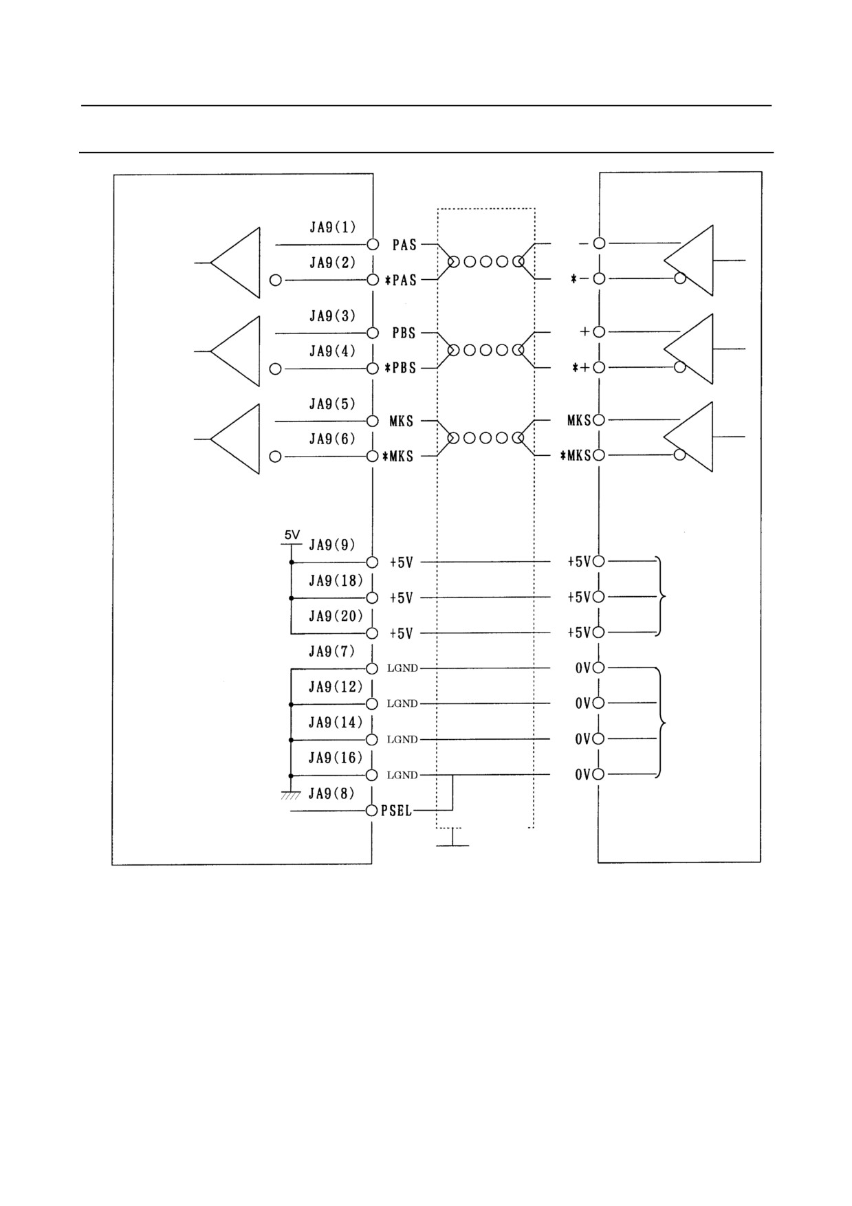
CONNECTION WITH PULSE GENERATOR
8.5.1
Use of Phase A and B Pulses
High-speed counter module
Pulse generator
Phase A
pulse signal
input
Phase B
pulse signal
input
Marker
signal input
Line receiver SN75115
Line receiver SN75113
Use these
lines together.
Use these
lines together.
Shield
Grounding plate
(*) The maximum current rating for each 5-V output is 300 mA.
Recommended cable
A66L-0001-0286 (#20AWG×7, #24AWG×3 Pairs)
- 115 -
8.HIGH-SPEED COUNTER MODULE CONNECTION
B-61813E/06
8.5.2
Use of Positive/Negative Pulses
High-speed counter module
Pulse generator
Negative
pulse signal
input
Positive
pulse signal
input
Marker
signal input
Line receiver SN75113
Line receiver SN75115
Use these
lines together.
Use these
lines together.
Shield
Grounding plate
(*) The maximum current rating for each 5-V output is 300 mA.
Recommended cable
A66L-0001-0286 (#20AWG×8, #24AWG×3 Pairs)
- 116 -
B-61813E/06
CONNECTION 8.HIGH-SPEED COUNTER MODULE
8.6
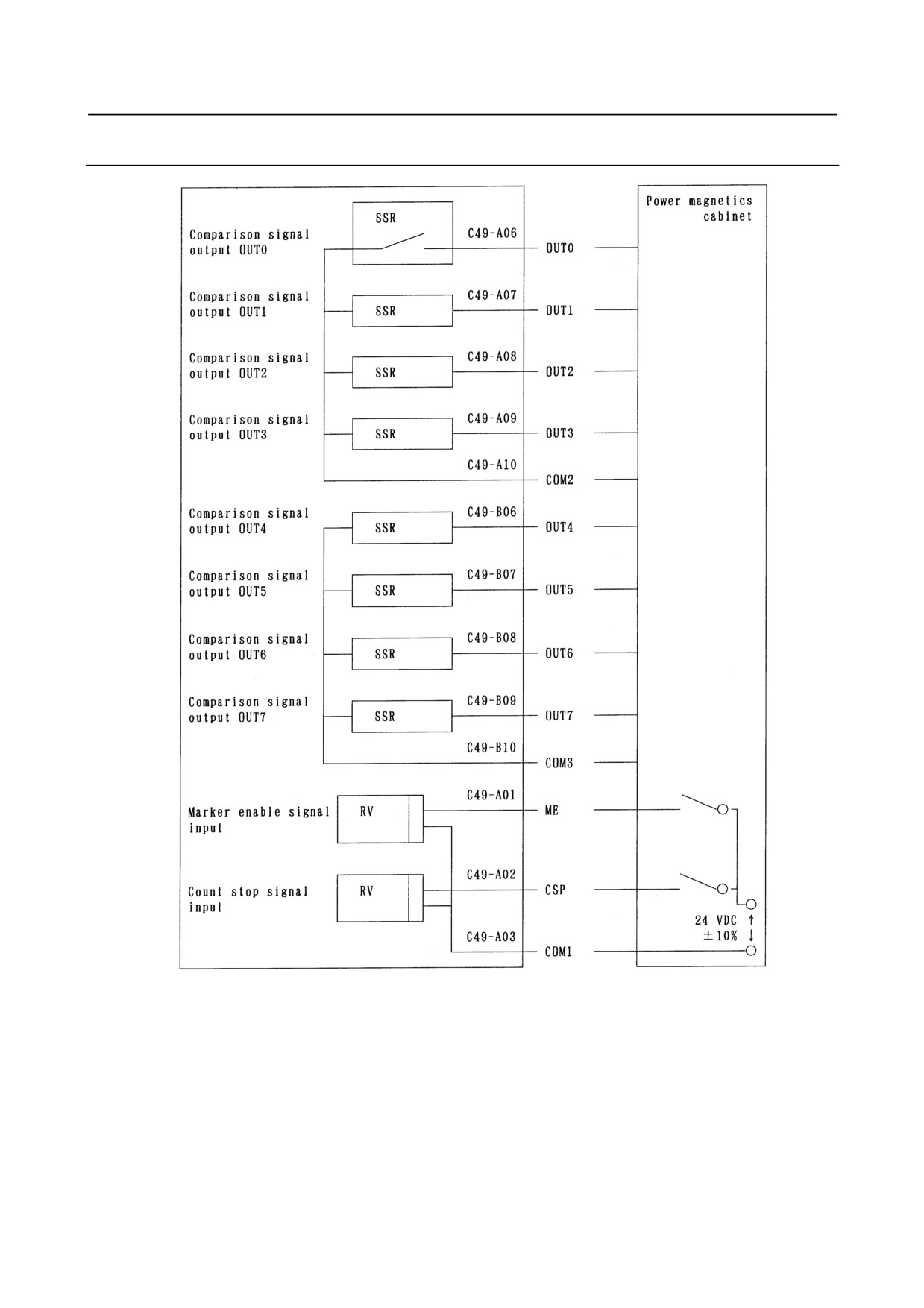
CONNECTION WITH MACHINE (POWER MAGNETICS
CABINET)
8.6.1
Use in Mode A
Machine (power
magnetics cabinet)
SSR
Comparison
C49-A06
CMP A
signal output
A
SSR
Comparison
C49-A07
signal output
CMPB
B
SSR
Comparison
C49-A08
signal output
CMPC
C
C49-A10
COM2
C49-A01
Marker enable
RV
ME
signal input
Count stop
C49-A02
RV
CSP
signal input
24VDC
↑
±10%
↓
C49-A03
COM1
- 117 -
8.HIGH-SPEED COUNTER MODULE CONNECTION
B-61813E/06
8.6.2
Use in Mode B
- 118 -
B-61813E/06
CONNECTION 8.HIGH-SPEED COUNTER MODULE
8.7
I/O SIGNALS CONVENTIONS
8.7.1
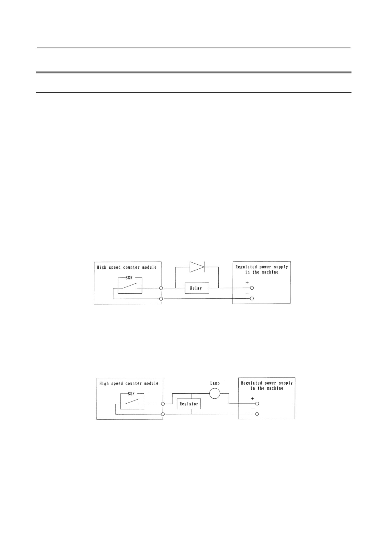
Solid State Relay Output Signals (OUT0 to OUT7)
The solid state relay output signals drive relays in the machine (power magnetics cabinet) side and indicator
LEDs.
(1) Solid state relays
(a) Maximum load current at output-on
250 mA: Up to three outputs set to on
125 mA: Eight outputs set to on
(b) Saturation voltage at output-on
Not more than 6 × IL [V] (IL: load current)
(c) Withstand voltage at output-off
30 VDC max. even for instantaneous voltage
(d) Leak current at output-off
Not more than 100μA
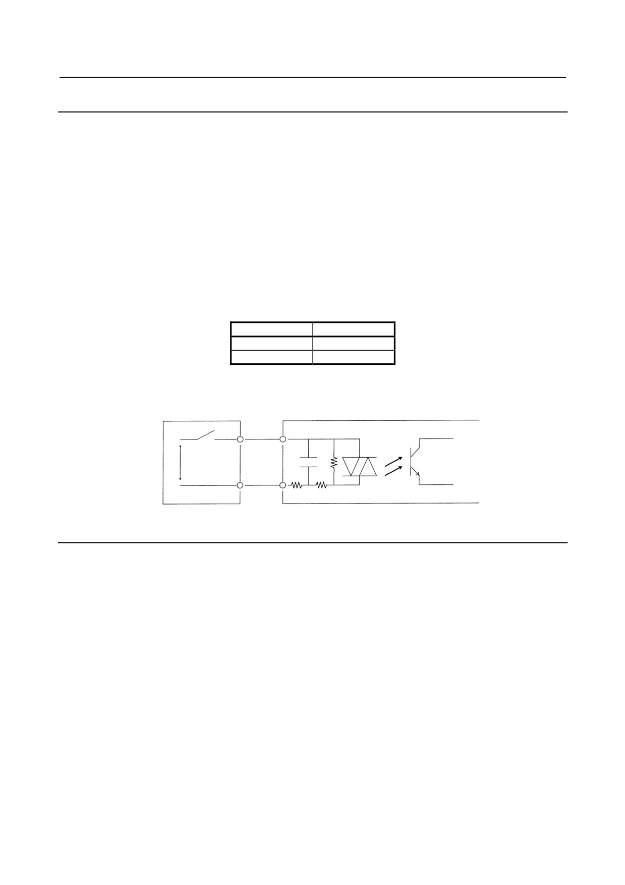
(2) Output circuit
(3) Always install surge arresters when inductive loads such as relays are connected in the machine. Insert
the surge arresters as near the load as possible (less than 20 cm). When capacitive loads are used in the
machine, insert current limiting resistors in series with the loads to prevent the instantaneous current
and voltage from exceeding the rated values.
(4) If a lamp is turned on by a solid state relay output, the resulting surge current may damage the solid
state relay. Thus, as shown in the figure below, provide a protective resistor to prevent the
instantaneous current and voltage from exceeding the rated values.
- 119 -
8.HIGH-SPEED COUNTER MODULE CONNECTION
B-61813E/06
8.7.2
DC Input Signals (ME and CSP)
The DC input signals (such as relay contact signal) are sent from the machine (control circuit) to the
high-speed counter module.
(1) Input conditions
On voltage and current: 15 VDC or more, 4.5 mA or more
Off voltage and current: 6 VDC or less, 2 mA or less
Response time: 20 ms or less
(2) Voltage and polarity
Voltage
:
24 VDC +10%, -20%
Polarity
: Positive or negative polarity available (The power is not supplied from the high-speed
counter module.)
(3) Logical correspondence
Contact
Logic
Open
0
Closed
1
(4) Receiver circuit of DC input signal
Machine
Pulse counter module
24VDC
+10%, -20%
8.7.3
+5-V Output from JA9 Connector
• A voltage of +5 V on the JA9 connector of this module is the output of the counter module (300 mA
maximum).
It is necessary to satisfy Table 4.4 in Section 4.4, "Required Current", though.
Example:
Assuming that 100 mA is supplied from the +5-V pin of the JA9 connector:170 + 0.3 × 100 = 200
Thus, the required current is 200 mA.
- 120 -
B-61813E/06
CONNECTION 8.HIGH-SPEED COUNTER MODULE
8.8
SUPPLEMENT
8.8.1
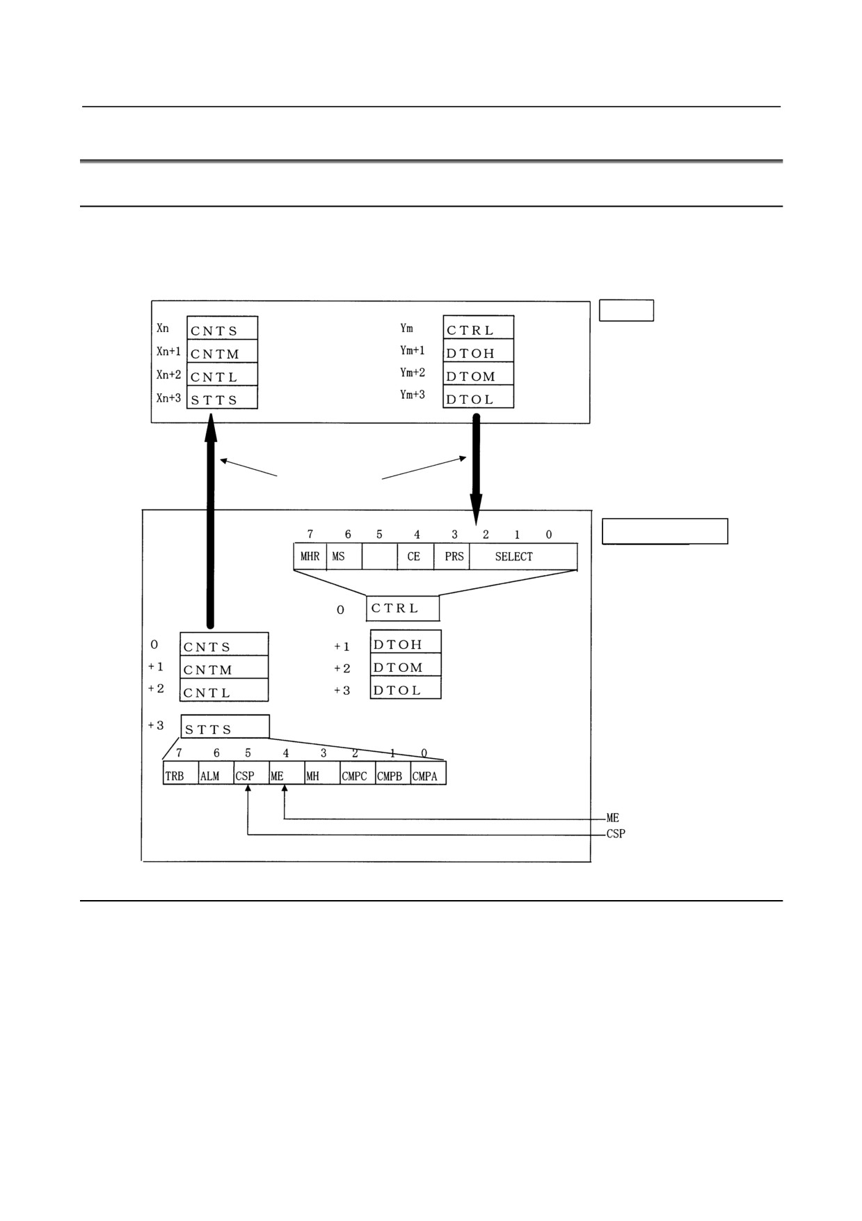
Configuration of Mode A
How mode A is configured is shown below. The contents of the CNTS, CNTM, CNTL, and STTS on a
high-speed counter module are sent to the X area assigned on the master via the I/O Link i or I/O Link. The
contents of the Y area assigned on the master are sent to CTRL, DTOH, DTOM, and DTOL on the
high-speed counter module, via the I/O Link i or I/O Link.
Master
Via the I/O Link i
or I/O Link
(period of 2 ms)
High-speed counter
8.8.2
Counter Presetting and Counting
(1) Presetting a counter value (using the external signal MKS)
To preset a counter value, using the MKS signal, follow this procedure:
(a) Reset the MH (marker hold) signal.
(b) Preset a value in the counter at the rising edge of the MKS signal.
The MH signal is set at the same time the counter is preset with data.
(a) Resetting the MH signal
For mode A, both methods, (i) and (ii), are usable. For mode B, method (ii) is usable.
(i)
Resetting the MS bit (bit 6) of the CTRL (control) register to 0
Control example 1
(ii) Setting the MHR bit (bit 7) of the CTRL register to 1
Control example 2
- 121 -
8.HIGH-SPEED COUNTER MODULE CONNECTION
B-61813E/06
Condition
Status
MHR of
ME of external
MKS of
MS of CTRL
ME of STTS
MH of STTS
CTRL
signal
external signal
(i)
×
0
×
×
×
Changes to 0.
(ii)
1
×
×
×
×
Changes to 0.
• The cross × in the above table means that the corresponding bit can be either 0 or 1.
(The ME bit of the STTS register corresponds to the state of the external signal ME.)
(b) Presetting a counter value
For both methods, (i) and (ii), the presetting is completed within 100 μs after the MKS has arisen.
Condition
Status
MHR of
ME of external
MKS of
MS of CTRL
ME of STTS
MH of STTS
CTRL
signal
external signal
Contact
(i), (ii)
0
1
First ↑ state
1
1
"Closed"
• Contact "Closed" in the above table means that 24 V is applied to the ME pin.
(2) Presetting a counter value (operating the PRS bit by ladder)
<1> Load the 3 low-order CTRL bits (SELECT) with 001 by ladder.
<2> Preset the DTOH, DTOM, and DTOL by ladder.
<3> Invert the PRS bit by ladder.
(If the PRS is 0, set it to 1. If it is 1, reset it to 0.)
NOTE
1 Once the PRS bit has been inverted, do not change the content of the DTOH,
DTOM, DTOL, or CTRL within the period of two ladder cycle scans.
Also do not invert the PRS bit again within the same period.
2 It takes about 5 ms for the counter to be preset since the inversion of the PRS bit.
Control example 1:
(Hatching
means that the bit can be either 0 or 1.)
Counter
Preset
Preset
Control example 2:
(Hatching
means that the bit can be either 0 or 1.)
Counter
Preset
Preset
- 122 -
B-61813E/06
CONNECTION 8.HIGH-SPEED COUNTER MODULE
(3) Count
The following table lists the conditions for counting by this module.
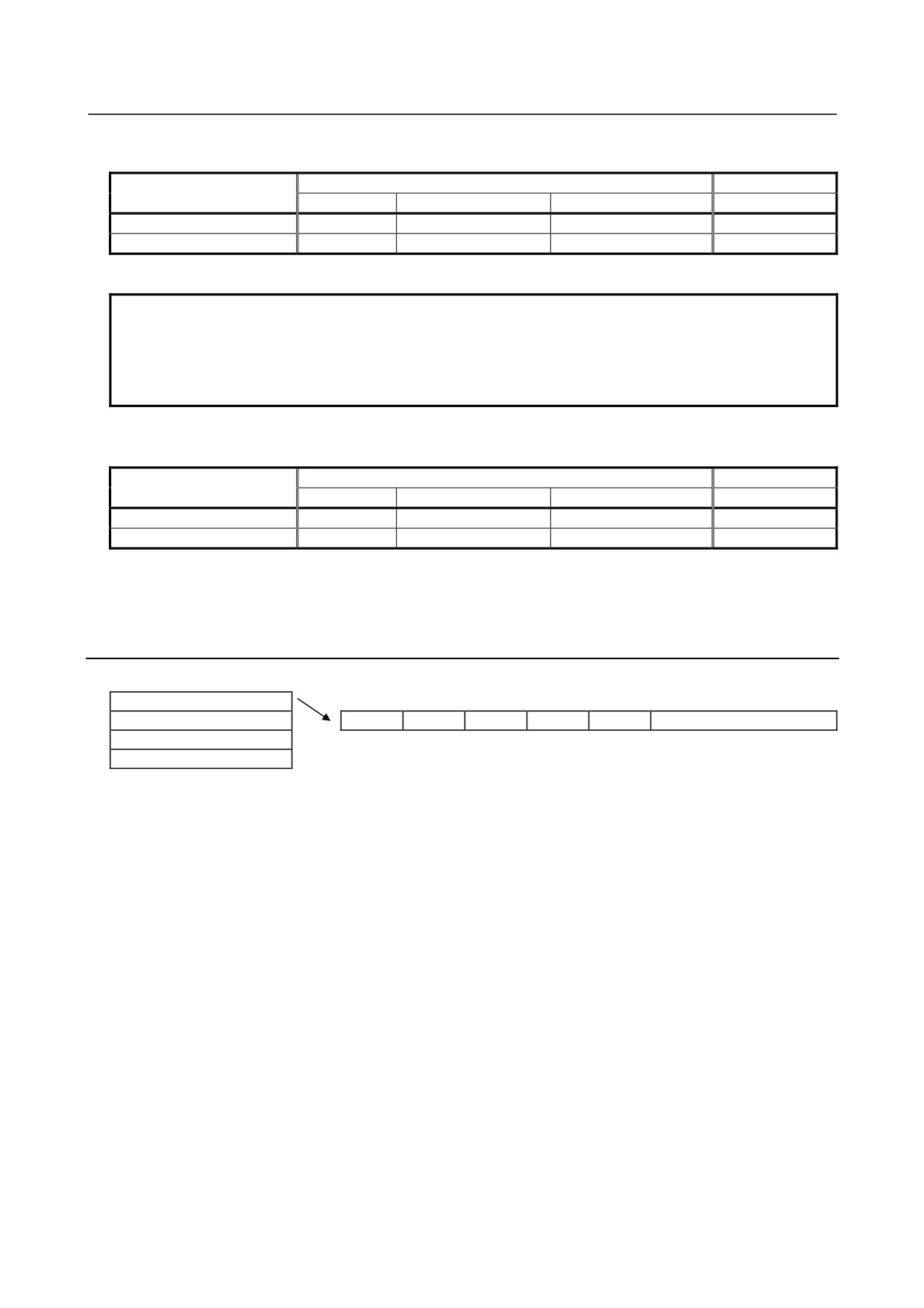
Condition
Status
CE of CTRL
CSP of external signal
PSEL of external signal
CSP of STTS
Count (A/B phase pulse)
1
Contact "Open"
Open
Reset to 0.
Count (+/- pulse)
1
Contact "Open"
Connected to 0 V
Reset to 0.
• Contact "Open" in the above table means that the CSP pin is open (0 or NEG).
NOTE
The count value does not become negative. The highest-order bit of the CNTS
register is the TRA bit (see Subsection 8.8.4).
Count-down: +1(00 0001H)→0(00 0000H)→+8,388,607(7F FFFFH) →
+8,388,606(7F FFFEH)
(4) Stopping counting
The following table lists the condition for this module to stop counting.
Condition
Status
CE of CTRL
CSP of external signal
PSEL of external signal
CSP of STTS
Count stop method 1
0
×
×
×
Count stop method 2
×
Contact “Closed”
×
Reset to 1.
• Contact “Closed” in the above table means that 24 V is applied to the CSP pin (1 or POS).
• The cross × in the above table means that the corresponding bit can be either 0 or 1.
(The × state of the CSP pin of the STTS register corresponds to the state of the external signal CSP.)
8.8.3
Setting Data
[Example of setting]
CTRL
7
6
5
4
3
2
1
0
DTOH
PRS
SELECT
DTOM
DTOL
Example 1 :
To preset the counter preset register with a specific value (the counter is also set to preset value),
follow the steps below.
(1) Preset the DTOH, DTOM, and DTOL with a desired value.
(2) Set SELECT to 001.
(3) Reverse the setting of the PRS (from 0 to 1 or from 1 to 0).
(4) Wait for two scanning periods.
• Another method for presetting the counter is to use the MKS external signal (see Subsection
8.8.2). It takes a maximum of 5 ms to preset using the first method, while it takes only a
maximum of 100 μs to preset using the MKS external signal.
Example 2 :
To set the comparison control register with the setting (0 or 1) of CMA, CMB, and CMC, follow the
steps below.
(1) Set DTOH bits 0, 1, and 2 to the desired data.
(2) Set SELECT to 000.
(3) Reverse the setting of the PRS (from 0 to 1 or from 1 to 0).
(4) Wait for two scanning periods.
- 123 -
8.HIGH-SPEED COUNTER MODULE CONNECTION
B-61813E/06
Example 3 :
To set comparison register B to a desired comparison value, follow the steps below.
(1) Set DTOH, DTOM, and DTOL to the desired comparison value.
(2) Set SELECT to 011.
(3) Reverse the setting of the PRS (from 0 to 1 or from 1 to 0).
(4) Wait for two scanning periods.
The result of comparing comparison registers A, B, and C with the pulse counter is output via OUT0 to
OUT2 of connector C49 of this counter module (A → OUT0, B → OUT1, and C → OUT2).
Their output status is output via OUT0 to OUT2 of the LED indication panel (A → OUT0, B → OUT1, and
C → OUT2).
The result of comparison can be confirmed by checking STTS bits 0, 1, and 2 (CMPA, CMPB, and CMPC)
with the PMC.
8.8.4
Reading Data
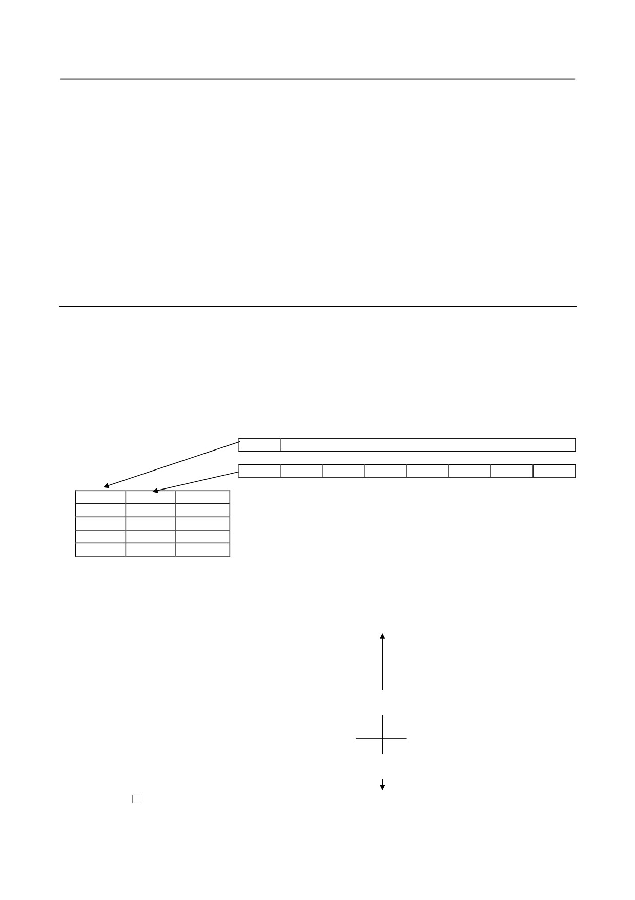
The CNTS and STTS are two of the four input bytes. The most significant bit, TRA, of the CNTS and the
most significant bit, TRB, of the STTS can be used to determine whether the count data is correct. If both
TRA and TRB are 0 or 1, the count data is correct. The time during which the TRA and TRB bits
have a different value from each other is about 2 msec.
In almost all cases, both TRA and TRB will be 0 or 1 when you view the diagnostic display. (Do not
determine that the data has not changed because of the fact that the TRA and TRB do not become 0 or 1
alternately.) Note that the count data does not take a negative value.
(CNTS)
TRA
Counter H
(STTS)
TRB
ALM
CSP
ME
MH
CMPC
CMPB
CMPA
The TRA and TRB bits provide timing signals used to check count data. The
TRA
TRB
Validity
count data is 3 bytes. After sent to the host via the I/O Link, its 2 bytes (CNTS
0
0
Correct
and CNTM bytes) are first written to memory. If the count data is accessed at
0
1
Incorrect
this moment, it does not represent a true value because the CNTL remains in
1
0
Incorrect
the previous state. Both the TRA and TRB bits become 0 or 1 only after all 4
1
1
Correct
bytes (3 count data bytes + 1 STTS byte) are written to memory.
The counter assumes the following data when it is incremented or decremented.
Contents of [ CNTS
CNTM CNTL ]
□0000000
00000000
00000010
□0000000
00000000
00000001
□0000000
00000000
00000000
□1111111
11111111
11111111
to
□0000000
00000000
00000011
Increment
□0000000
00000000
00000010
□0000000
00000000
00000001
□0000000
00000000
00000000
□1111111
11111111
11111111
Decrement
□1111111
11111111
11111110
□1111111
11111111
11111101
The square
represents the TRA. (The most significant bit is the TRA. It is not a sign bit.)
- 124 -