Intel 64 and IA-32 Architectures. Software Developer’s Manual (Collection, 2023) - page 147

INTEL® ADVANCED MATRIX EXTENSIONS (INTEL® AMX)
/* 2 of 3 */
/// This intrinsic corresponds to the <c> TDPBSSD </c> instruction.
///
/// \param dst
/// The destination tile. Max size is 1024 Bytes.
/// \param src0
/// The 1st source tile. Max size is 1024 Bytes.
/// \param src1
/// The 2nd source tile. Max size is 1024 Bytes.
void __tile_dpbssd(__tile1024i *dst, __tile1024i src1, __tile1024i src2);
/// Compute dot-product of bytes in tiles with a source/destination accumulator.
/// Multiply groups of 4 adjacent pairs of signed 8-bit integers in src0 with
/// corresponding unsigned 8-bit integers in src1, producing 4 intermediate
/// 32-bit results. Sum these 4 results with the corresponding 32-bit integer
/// in "dst", and store the 32-bit result back to tile "dst".
///
/// \headerfile <immintrin.h>
///
/// This intrinsic corresponds to the <c> TDPBSUD </c> instruction.
///
/// \param dst
/// The destination tile. Max size is 1024 Bytes.
/// \param src0
/// The 1st source tile. Max size is 1024 Bytes.
/// \param src1
/// The 2nd source tile. Max size is 1024 Bytes.
void __tile_dpbsud(__tile1024i *dst, __tile1024i src1, __tile1024i src2);
/// Compute dot-product of bytes in tiles with a source/destination accumulator.
/// Multiply groups of 4 adjacent pairs of unsigned 8-bit integers in src0 with
/// corresponding signed 8-bit integers in src1, producing 4 intermediate 32-bit
/// results. Sum these 4 results with the corresponding 32-bit integer in "dst",
/// and store the 32-bit result back to tile "dst".
///
/// \headerfile <immintrin.h>
///
/// This intrinsic corresponds to the <c> TDPBUUD </c> instruction.
///
/// \param dst
/// The destination tile. Max size is 1024 Bytes.
/// \param src0
/// The 1st source tile. Max size is 1024 Bytes.
/// \param src1
/// The 2nd source tile. Max size is 1024 Bytes.
void __tile_dpbuud(__tile1024i *dst, __tile1024i src1, __tile1024i src2);
/// Zero the tile specified by "dst".
///
/// \headerfile <immintrin.h>
///
20-60

INTEL® ADVANCED MATRIX EXTENSIONS (INTEL® AMX)
/* 2of 2 */
/// This intrinsic corresponds to the <c> TILEZERO </c> instruction.
///
/// \param dst
/// The destination tile to be zero. Max size is 1024 Bytes.
void __tile_zero(__tile1024i* dst);
/// Compute dot-product of BF16 (16-bit) floating-point pairs in tiles src0 and
/// src1, accumulating the intermediate single-precision (32-bit) floating-point
/// elements with elements in "dst", and store the 32-bit result back to tile
/// "dst".
///
/// \headerfile <immintrin.h>
///
/// This intrinsic corresponds to the <c> TDPBF16PS </c> instruction.
////// \param dst
/// The destination tile. Max size is 1024 Bytes.
/// \param src0
/// The 1st source tile. Max size is 1024 Bytes.
/// \param src1
/// The 2nd source tile. Max size is 1024 Bytes.
void __tile_dpbf16ps(__tile1024i* dst, __tile1024i src0, __tile1024i src1);
/// Store the tile specified by "src" to memory specified by "base" address and
/// "stride".
///
/// \headerfile <immintrin.h>
///
/// This intrinsic corresponds to the <c> TILESTORED </c> instruction.
///
/// \param dst
/// A destination tile. Max size is 1024 Bytes.
/// \param base
/// A pointer to base address.
/// \param stride
/// The stride between the rows' data to be stored in memory.
void __tile_stored(void *base, __SIZE_TYPE__ stride, __tile1024i src);
20-61

INTEL® ADVANCED MATRIX EXTENSIONS (INTEL® AMX)
20.18.4 INTEL® AMX INTRINSICS EXAMPLE
In Example 20-30, function foo is called in line 18, and the tile variable ‘a’ written in line 17 needs to live
up to line 21 across the function call. The compiler needs to save the tile data register allocated to ‘a’
before calling foo, then restore the tile configure register and tile data registers after calling foo. Lines 39,
42, and 46 in Example 20-31 are the save/restore code. Since the configure register doesn’t change, the
configure register in the stack does not require saving.
Example 20-30. Intel® AMX Intrinsics Usage
1 #include <immintrin.h>
2
3 char buf[1024];
4 #define STRIDE 32
5
6 int count = 0;
7 __attribute__((noinline))
8 void foo() {
9 count++;
10 }
11
12 void test_api(int cond, unsigned short row, unsigned short col) {
13
__tile1024i a = {row, col};
14
__tile1024i b = {row, col};
15
__tile1024i c = {row, col};
16
17
__tile_loadd(&a, buf, STRIDE);
18 foo();
19
__tile_loadd(&b, buf, STRIDE);
20
__tile_loadd(&c, buf, STRIDE);
21
__tile_dpbssd(&c, a, b);
22
__tile_stored(buf, STRIDE, c);
23 }
clang -O2 -S amx-across-func.c -mamx-int8 -mavx512f -fno-asynchronous-unwind-tables.
Notice the ldtilecfg instruction at the beginning of the function (line 34 in Example 20-31), which sets the
Intel AMX registers configuration within the CPU and the TileRelease instruction towards the end of the
function. This placement ensures that the Intel AMX state is initialized, thus avoiding the expensive Intel
AMX state save/restore in case of a software thread context-switch outside of the Intel AMX function.
20-62

INTEL® ADVANCED MATRIX EXTENSIONS (INTEL® AMX)
Example 20-31. Compiler-Generated Assembly-Level Code from Example 20-30
16 test_api:
# @test_api
17 # %bb.0:
# %entry
18
pushq
%rbp
19
pushq
%r15
20
pushq
%r14
21
pushq
%rbx
22
subq
$1096, %rsp
# imm = 0x448
23
movl
%edx, %ebx
24
movl
%esi, %ebp
25
vpxord %zmm0, %zmm0, %zmm0
26
vmovdqu64
%zmm0, (%rsp)
27
movb
$1, (%rsp)
28
movw
%bx, 20(%rsp)
29
movb
%bpl, 50(%rsp)
30
movw
%bx, 18(%rsp)
31
movb
%bpl, 49(%rsp)
32
movw
%bx, 16(%rsp)
33
movb
%bpl, 48(%rsp)
34
ldtilecfg
(%rsp)
35
movl
$buf, %r14d
36
movl
$32, %r15d
37
tileloadd
(%r14,%r15), %tmm0
38
movabsq $64, %rax
39
tilestored
%tmm0, 64(%rsp,%rax)
# 1024-byte Folded Spill
40
vzeroupper
41
callq foo
42
ldtilecfg
(%rsp)
43
tileloadd
(%r14,%r15), %tmm0
44
tileloadd
(%r14,%r15), %tmm1
45
movabsq $64, %rax
46
tileloadd
64(%rsp,%rax), %tmm2
# 1024-byte Folded Reload
47
tdpbssd %tmm0, %tmm2, %tmm1
48
tilestored
%tmm1, (%r14,%r15)
49
addq
$1096, %rsp
# imm = 0x448
50
popq
%rbx
51
popq
%r14
52
popq
%r15
53
popq
%rbp
54
tilerelease
55
retq
20.18.5 COMPILATION OPTION
The save/restore is sometimes unnecessary, e.g., when foo does not clobber any tile register. To avoid
unnecessary save/restore, compile with “-mllvm -enable-ipra”, which does an IPO analysis to get the
information on what physical registers are clobbered during the function call. Example 20-32 shows no
tile register save/restore across calling foo.
clang -O2 -S amx-across-func.c -mamx-int8 -mavx512f -fno-asynchronous-unwind-tables -mllvm -
enable-ipra
20-63

INTEL® ADVANCED MATRIX EXTENSIONS (INTEL® AMX)
Example 20-32. Compiler-Generated Assembly-Level Code Where Tile Register Save/Restore is Optimized Away
15
.type test_api,@function
16 test_api:
# @test_api
17 # %bb.0:
# %entry
18
subq
$72, %rsp
19
vpxord %zmm0, %zmm0, %zmm0
20
vmovdqu64
%zmm0, 8(%rsp)
21
movb
$1, 8(%rsp)
22
movw
%dx, 28(%rsp)
23
movb
%sil, 58(%rsp)
24
movw
%dx, 26(%rsp)
25
movb
%sil, 57(%rsp)
26
movw
%dx, 24(%rsp)
27
movb
%sil, 56(%rsp)
28
ldtilecfg
8(%rsp)
29
movl
$buf, %eax
30
movl
$32, %ecx
31
tileloadd
(%rax,%rcx), %tmm0
32
callq foo
33
tileloadd
(%rax,%rcx), %tmm1
34
tileloadd
(%rax,%rcx), %tmm2
35
tdpbssd %tmm1, %tmm0, %tmm2
36
tilestored
%tmm2, (%rax,%rcx)
37
addq
$72, %rsp
38
tilerelease
39
vzeroupper
40
retq
41 .Lfunc_end1:
42
.size test_api, .Lfunc_end1-test_api
20.19 INTEL® AMX STATE MANAGEMENT
Intel AMX is XSAVE supported, meaning that it defines processor registers that can be saved and
restored using instructions of the XSAVE feature set. Intel AMX is also XSAVE enabled, meaning that
system software must enable it before it can be used.
The XSAVE feature set operates on state components, each a discrete set of processor registers (or parts
of registers). Intel AMX is associated with two state components, XTILECFG and XTILEDATA. The XSAVE
feature set organizes state components using state-component bitmaps. A state-component bitmap
comprises 64 bits; each bit in such a bitmap corresponds to a single state component. Intel AMX defines
bits 18:17 for its state components (collectively, these are called AMX state):
• State component 17 is used for the 64-byte TILECFG register (XTILECFG state).
• State component 18 is used for the 8192 bytes of tile data (XTILEDATA state).
These are both user-state components, meaning the entire XSAVE feature set can manage them. In
addition, it implies that setting bits 18:17 of extended control register XCR0 by system software enables
Intel AMX. If those bits are zero, an Intel AMX instruction execution results in an invalid-opcode excep-
tion (#UD).
About the XSAVE feature set’s INIT optimization, the Intel AMX state is in its initial configuration if the
TILECFG register is zero and all tile data are zero.
Enumeration and feature-enabling documentation can be found in Section 20.2.
20-64

INTEL® ADVANCED MATRIX EXTENSIONS (INTEL® AMX)
An execution of XRSTOR or XRSTORS initializes the TILECFG register (resulting in TILES_CONFIGURED =
0) in response to an attempt to load it with an illegal value. Moreover, an execution of XRSTOR or
XRSTORS that is not directed to load XTILEDATA leaves it unmodified, even if the execution is loading
XTILECFG.
It is highly recommended that developers execute TILERELEASE to initialize the tiles at the end of the
Intel AMX instructions code region. More on this is in Section 20.18.
If the system software does not initialize the Intel AMX state first (by executing TILERELEASE, for
example), it may disable Intel AMX by clearing XCR0[18:17], by clearing CR4.OSXSAVE, or by setting
IA32_XFD[18].
20.19.1 EXTENDED FEATURE DISABLE (XFD)
The XTILEDATA state component size is 8 KBytes, and an operating system may, by default, prefer not to
allocate memory for the XTILEDATA state for every user thread. An operating system that enables Intel
AMX might select a fault when user threads use the feature. That way, it can allocate a large enough state
save area only for the user threads using the feature. An operating system may offer an API for the user
threads to declare their intention to use Intel AMX and allow the OS to preallocate the state and avoid an
exception when Intel AMX is used for the first time.
See Linux API and Windows API for more details.
Extended feature disable (XFD) is added to the XSAVE feature set to support such usage. See the Intel®
AMX Architecture Definition for XFD documentation.
20.19.2 ALTERNATE SIGNAL HANDLER STACK IN LINUX OPERATING SYSTEM
When programs use an alternate signal handler stack, the stack size should be adjusted to accommodate
the additional Intel AMX state. See Using XSTATE Features in User-Space Applications for more details.
20.20 USING INTEL® AMX TO EMULATE HIGHER PRECISION GEMMS
Intel AMX/TMUL has instructions that enable matrix-matrix operations such as multiplication on small
precision elements. This section considers how to use the low-precision Intel AMX instructions to approx-
imate the answers to matrix-matrix multiplication of higher-precision terms. Even if low-precision inputs
are Bfloat16 or Integer8, one can still combine the transforms to approximate matrix-matrix multiplica-
tion in higher precisions.
Pay attention to the exponent range and mantissa bits when approximating higher precisions. There are
IEEE-754 double precision numbers (FP64) that aren’t representable as single precision (FP32) or lower
precisions. These are typically range-based issues in the exponent bits. FP64 has more exponent bits
than FP32. However, scaling factors can overcome most range-based problems. If A is a matrix of FP64
values, then A (as a sum of Bfloat16 matrices) cannot generally be represented. Scaling factors can,
however, be used to get around most issues. The A-matrix as s1*A1 + s2*A2 + … + sn*An can be written
where each matrix A_i is lower precision, and each si is a constant scaling factor.
For Bfloat16 decomposition of FP32, consider the following:
• Let A be a matrix of FP32 values.
• Let A1 = bfloat16(A), a matrix containing RNE-rounded Bfloat16 conversions of A.
• Let A2 = bfloat16(A - fp32(A1)).
• Let A3 = bfloat16(A - fp32(A1) - fp32(A2)).
• Now A is approximately A1 + A2 + A3.
20-65
INTEL® ADVANCED MATRIX EXTENSIONS (INTEL® AMX)
Once one has written two matrices as a sum of lower precision matrices, one can run AMX/TMUL on the
product to approximate the higher precision. But to do this effectively, one needs to have higher precision
accumulation. There are tricks in the literature for doing higher precision all in a lower precision, such as
works on so-called double-double arithmetic. Still, these tend to vary too much from standard matrix-
matrix multiplication to be helpful with TMUL. In the case of Bfloat16, having 32-bit accumulation in the
product allows one to use Bfloat16 to approximate FP32 accuracy.
Therefore, if A = s1*A1 + s2*A2 + s3*A3, and B = t1*B1 + t2*B2 + t3*B3, then A*B can be computed
using AMX/TMUL on the projects Ai*Bj for 1<=i,j<=3, assuming scaling is done carefully to avoid denor-
mals. Assuming FP32 accumulation, the FP32 approximation of A*B can be made by writing out these
lower precision multiplies. Scaling factors can be chosen to avoid denormals at times, but they can also
be picked in a way that simplifies further steps in the algorithm. In some cases, scaling factors can be
chosen to be a power of two, for instance, without significantly reducing the accuracy of the resulting
matrix-matrix multiply.
The number of matrices for A or B are picked depending on the mantissa range to cover. If trying to
emulate FP32 which has 24 bits of mantissa (including the implicit mantissa bit), it is possible with three
Bfloat16 matrices (because each of the triples has 8 bits of mantissa, including the implicit bit.). Here the
range is less important because Bfloat16 and FP32 have the same exponent range. Use three Bfloat16
matrices to approximate FP32 precision by BF16x3. Range issues may still come up for BF16x3 cases
where A has values close to the maximum or minimum exponent for FP32, but that too can be circum-
vented by scaling constants. Scaling factors of 2^24 or 2^(-24) suffice to push it far enough away from
the boundary to make the computation feasible again. This is dependent upon the closest end of the
spectrum.
A few terms from an expansion can also be dropped. For instance, in the BF16x3 case, where there are
three As and three Bs, nine products may result. That is:
A*B = (A1+A2+A3)*(B1+B2+B3) = (A1*B1) + (A1*B2 + A2*B1) + (A1*B3 + A2*B2 + A3*B1) +
(A2*B3 + A3*B2) +(A3*B3).
The parentheses in the last equation are intentionally derived so that all entries in the same “bin” are put
together, and there are nine entries of the form Ai*Bj. This example has five bins, each with its own set
of parentheses. In the Bfloat16 case, |Ai| <= |A_i-1}| / 256. This shows the last two bins (with
A2*B3,A3*B2,A3*B3) are too small to contribute significantly to the answer, which is why if there are Y
terms on each side of A*B, only (Y+1)*Y/2 multiplies are required, not Y*Y multiplies. In this case, drop-
ping the last three (also the difference between Y*Y - (Y+1)*Y/2 when Y=3.) from the nine multiplies.
The last three multiplies in the last two bins have terms less than 2^(-24) as big as the first term. So,
A*B can be approximated (ignoring the scaling terms for now) as the sum of the first three most signifi-
cant bins: A1*B1 + (A1*B2+A2*B1)+(A1*B3+A2*B2*A3*B1). In this case, adding from the least signif-
icant bin to the most significant bin (A1*B1) is recommended.
Whenever A and B are each expanded out to Y-terms, computing only Y*(Y+1)/2 products works under
the condition that each term has the same number of mantissa bits. If some terms have a different
number of bits, then this guideline no longer applies. But for BF16x3, each term covers eight mantissa
bits and Y=3, so six products are needed.
Regarding accuracy, the worst-case relative error for BF16x3 may be worse than FP32. However, BF16x3
tends to cover a larger mantissa range due to implicit bits, which can be more accurate in many cases.
Nevertheless, accuracy is not offered by matrix-matrix multiplication. Even FP64 or FP128 can be bad for
component-wise relative errors. Take A = [1, -1] and B = [1; 1]. A*B is zero. Let eps be a small pertur-
bation to A and/or B. The solution may now be arbitrarily bad in terms of relative error. In general,
assume that the same mantissa range and exponent range is covered as a given higher-precision floating
point format, and the accumulation is at least as good as the higher-precision format. With such an
assumption, the answer will be approximately the same as the higher-precision floating point format. It
may or may not be identical. Performing the same operation in the higher precision format but changing
the order of the computations could yield slightly different results. In terms of matrix-matrix multiplica-
tion, it could yield vast differences in relative error.
20-66

INTEL® ADVANCED MATRIX EXTENSIONS (INTEL® AMX)
Things get slightly more complicated if low precision is used to approximate matrix-matrix at FP64 accu-
racy or FP128 precision. Here the scalars aren’t just for avoiding denormals but are necessary to do the
initial matrix conversion. Nevertheless, converting to an integer is recommended in this case because the
FP32-rounded errors in each of the seven or fewer bins may introduce too many errors. An integer is
easier to get right because there are no floating-point errors in each bin.
Conversion to Integer functions in the same way as all of the previous Bfloat16 examples. The quantiza-
tion literature explains how to map floating point numbers into integers. The only difference is that these
integers are further broken down into 8-bit pieces for the use of AMX. Constant factors are still needed,
but in this case they are primarily defined in the conversion itself.
One difficulty with quantization to integers is the notion of a shared exponent. All the numbers quantized
together with shared exponents must share the same range. The assumption is that all of A shares a joint
exponent range. Since this will also be true for B, each row of A and column of B can be quantized sepa-
rately.
Assuming that there is Integer32 accumulation with the Integer8 multiplies, a matrix may be broken
down into far more bits than required. This may significantly reduce the inaccuracy impact of picking a
shared exponent. Because Integer32 arithmetic will be precise, modulo overflow/underflow concerns,
then one can break up A or B into a huge number of 8-bit integer matrices, then do all the matrix-matrix
work with AMX, and then convert back all the results to even get accuracies up to quad-precision.
Considering an extreme case of trying to get over 100-bits of accuracy in a matrix-matrix multiply. All A-
values can be quantified into 128-bit integers. The same holds true with B. Once broken down into 8-bit
quantities, this will have a significant expansion like: A = s1*A1 + s2*A2 + … + s14*A14 for when
attempting 112-bits of mantissa. The same can be done with B = t1*B1 + t2*B2 + … + t14*B14. A*B is
potentially 14*14=196 products, but only 105 products are needed because the last few products may
have scaling factors less than 2^(-112) times the most important terms. Each product term should be
added separately and computing into C from the least significant bits forward.
C15 = (s1*t14)*A1*B14 + (s2*t13)*A2*B13 + … + (s14*t1)*A14*B1
C14 = (s1*t13)*A1*B13 + (s2*t12)*A2*B12 + … + (s13*t1)*A13*B1
C13 = (s1*t12)*A1*B12 + (s2*t11)*A2*B11 + … + (s12*t1)*A12*B1
…
C02 = (s1*t1)*A1*B1
Sometimes choosing scalers is possible such that all the products in a given row can be computed with
the same scratch array. The converted sum of C02 gives the final product through C15, where terms like
C15 should be computed first.
Writing matrix-matrix multiplies in terms of an expansion like (A1+A2+A3)*(B1+B2+B3) is referred to
as “cascading GEMM.” Performance will vary depending on the TMUL/AMX specification, and may vary
from generation to generation. Note that some computations may become bandwidth-bound. Since
there is no quad floating-point precision in hardware for Intel Architecture, the above algorithm may be
competitive performance-wise with other approaches like doing software double-double optimizations or
software-based quad precision.
20-67

Intel® 64 and IA-32 Architectures
Optimization Reference Manual
Documentation Changes
August 2023
Document Number: 355308-002

Contents
Revision History
4
Preface
5
Nomenclature
5
Summary Tables of Changes
5
Documentation Changes
5
Intel® 64 and IA-32 Architectures Optimization Reference Manual Documentation Changes
3

Revision History
Revision History
Revision
Description
Date
-001
Initial release
May 2023
-002
Q3 Release
August 2023
4
Intel® 64 and IA-32 Architectures Optimization Reference Manual Documentation Changes

Preface
This document is an update to the optimization recommendations contained in the Intel® 64 and IA-32
Architectures Optimization Reference Manual, also known as the Software Optimization Manual. This document
is a compilation of device and documentation errata, specification clarifications and changes. It is intended for
hardware system manufacturers and software developers of applications, operating systems, or tools.
Nomenclature
Documentation Changes include typos, errors, or omissions from the current published specifications. These
will be incorporated in any new release of the specification.
Summary Tables of Changes
The following table indicates documentation changes which apply to the Intel® 64 and IA-32 Architecture
software optimization topics covered by this reference manual.
No.
DOCUMENTATION CHANGES
1
Updates to Chapter 2
2
Updates to Chapter 3
3
Updates to Chapter 5
4
Updates to Chapter 20
5
Updates to Appendix E
6
Updates to Appendix F
7
Updates to Appendix D
Documentation Changes
Changes to the Intel® 64 and IA-32 Architectures Optimization Reference Manual volumes follow, and are listed
by chapter. Only chapters with changes are included in this document.
Intel® 64 and IA-32 Architectures Optimization Reference Manual Documentation Changes
5
1.
Updates to Chapter 2
Change bars and violet text show changes to Chapter 2 of the Intel® 64 and IA-32 Architectures Optimization
Reference Manual: Introduction.
------------------------------------------------------------------------------------------
Changes to this chapter:
• Section 2.3
— Updated Figure 2-1 to correct a typo
• Section 2.4:
— Updated Figure 2-3 to match style of 2-1
• Section 2.7
— Removed section Relating to Knights Landing: “Intel Xeon Phi processors based on the Knights Landing
microarchitecture support 4 logical processors in each processor core; see Chapter 23 for detailed
information of Intel HT Technology that is implemented in the Knights Landing microarchitecture.”
— Updated Figure 2-9 to match style of other Figures.
Intel® 64 and IA-32 Architectures Optimization Reference Manual Documentation Changes
6

INTEL® 64 AND IA-32 PROCESSOR ARCHITECTURES
CHAPTER 2
INTEL® 64 AND IA-32 PROCESSOR ARCHITECTURES
This chapter gives an overview of features relevant to software optimization for current generations of
Intel® 64 and IA-32 processors1. These features are:
• Microarchitectures that enable executing instructions with high throughput at high clock speeds, a
high-speed cache hierarchy, and high-speed system bus.
• Intel® Hyper-Threading Technology2 (Intel® HT Technology) support.
• Intel 64 architecture on Intel 64 processors.
• Single Instruction Multiple Data (SIMD) instruction extensions: MMX™ technology, Streaming SIMD
Extensions (Intel® SSE), Streaming SIMD Extensions 2 (Intel® SSE2), Streaming SIMD Extensions 3
(Intel® SSE3), Supplemental Streaming SIMD Extensions 3 (SSSE3), Intel® SSE4.1, and Intel®
SSE4.2.
• Intel® Advanced Vector Extensions (Intel® AVX).
• Half-precision floating-point conversion and RDRAND.
• Fused Multiply Add Extensions.
• Intel® Advanced Vector Extensions 2 (Intel® AVX2).
• ADX and RDSEED.
• Intel® Advanced Vector Extensions 512 (Intel® AVX-512).
• Intel® Thread Director.
2.1
SAPPHIRE RAPIDS MICROARCHITECTURE
Intel processors based on Sapphire Rapids microarchitecture use Golden Cove cores and support the
following additional features:
• Intel® Advanced Matrix Extensions (Intel® AMX) (Chapter 20).
• Intel® Advanced Vector Extensions 512 (Intel® AVX-512) (Chapter 19).
• Intel® Data Streaming Accelerator (Intel® DSA)3.
• Intel® In-Memory Analytics Accelerator (Intel® IAA)4.
• Intel® Quick Assist Technology (Intel® QAT)(Chapter 22)
2.1.1
4th Generation Intel® Xeon® Scalable Family of Processors
Intel's fourth generation Xeon® Scalable Family of Processors changes from a single-die monolithic
design to multi-die Tiles.
The server products are scalable from dual-socket to eight-socket configurations (Section 3.11).
The I/O is increased with PCI Express 5.0, DDR5 memory, and Compute Express Link 1.1.
Packaging includes a multi-die chip with up to 4 tiles. Each tile is a 400mm2 SoC, providing both compute
cores and I/O.
1. Intel Atom® processors are covered in Chapter 4, “Intel Atom® Processor Architectures.”
2. Intel HT Technology requires a computer system with an Intel processor supporting hyper-threading and an Intel HT
Technology-enabled chipset, BIOS, and operating system. Performance varies depending on the hardware and software
used.
3. Please see the Intel® DSA Specification and Intel® DSA User Guide.
4. Please see the Intel® IAA Specification.
Ref#: 248966-048
2-1
INTEL® 64 AND IA-32 PROCESSOR ARCHITECTURES
Each tile contains 15 Golden Cove cores (see Section 2.3). Its memory controller provides two channels
of DDR5 with a maximum of eight channels across 4 tiles, and 28 PCIe 5.0 lanes for a maximum of 112
across 4 tiles.
2.2
ALDER LAKE PERFORMANCE HYBRID ARCHITECTURE
The Alder Lake performance hybrid architecture combines two Intel architectures, bringing together the
Golden Cove performant cores and the Gracemont efficient Atom cores onto a single SoC. For details on
the Golden Cove microarchitecture, see Section 2.3 For details on the Gracemont microarchitecture, see
Section 4.1
2.2.1
12th Generation Intel® Core™ Processors Supporting Performance Hybrid
Architecture
12th Generation Intel® Core™ processors supporting performance hybrid architecture consist of up to
eight Performance cores (P-cores) and eight Efficient cores (E-cores). These processors also include a
3MB Last Level Cache (LLC) per IDI module, where a module is one P-core or four E-cores. It has
symmetrical ISA and comes in variety of configurations.
P-cores provide single or limited thread performance, while E-cores help provide improved scaling and
multithreaded efficiency. P-cores on these processors can also have Intel Hyper-Threading Technology
enabled. All cores can be active simultaneously when the operating system (OS) decides to schedule on
all processors.
A key OSV requirement for enabling hybrid is symmetric ISA across different core types in a performance
hybrid architecture. In 12th Generation Intel Core processors supporting performance hybrid architec-
ture, ISA is converged to a common baseline between the P-cores and E-cores. In order to maintain
symmetric ISA, the E-cores do not support the following features: Intel AVX-512, Intel AVX-512 FP-16,
and Intel® TSX. The E-cores do support Intel AVX2 and Intel AVX-VNNI.
2.2.2
Hybrid Scheduling
2.2.2.1
Intel® Thread Director
Intel® Thread Director continually monitors software in real-time giving hints to the operating system's
scheduler allowing it to make more intelligent and data-driven decisions on thread scheduling. With Intel
Thread Director, hardware provides runtime feedback to the OS per thread based on various IPC perfor-
mance characteristics, in the form of:
• Dynamic performance and energy efficiency capabilities of P-cores and E-cores based on
power/thermal limits.
• Idling hints when power and thermal are constrained.
Intel Thread Director is first introduced in desktop and mobile variants of the 12th generation Intel Core
processor based on Alder Lake performance hybrid architecture.
A processor containing both P-cores and E-cores with different performance characteristics creates a
challenge for the operating system’s scheduler. Additionally, different software threads see different
performance ratios between the P-cores and E-cores. For example, the performance ratio between the
P-cores and E-cores for highly vectorized floating-point code is higher than the performance ratio for
scalar integer code. So, when the operating system needs to make an optimal scheduling decision it
needs to be aware of the characteristics of the software threads that are candidates for scheduling. If not
enough P-cores are available and there is a mix of software threads with different characteristics, the
operating system should schedule those threads that benefit most from the P-cores onto those cores and
schedule the others on the E-cores.
Ref#: 248966-048
2-2

INTEL® 64 AND IA-32 PROCESSOR ARCHITECTURES
Intel Thread Director provides the necessary hint to the operating system about the characteristics of the
software thread executing on each of the logical processors. The hint is dynamic and reflects the recent
characteristics of the thread, i.e., it may change over time based on the dynamic instruction mix of the
thread. The processor also considers microarchitecture factors to define the dynamic software thread
characteristics.
Thread specific hardware support is enumerated via the CPUID instruction and enabled by the operating
system via writing to configuration MSRs. The Intel Thread Director implementation on processors based
on Alder Lake performance hybrid architecture defines four thread classes:
0. Non-vectorized integer or floating-point code.
1. Integer or floating-point vectorized code, excluding Intel® Deep Learning Boost (Intel® DL Boost)
code.
2. Intel DL Boost code.
3. Pause (spin-wait) dominated code.
The dynamic code does not have to be 100% of the class definition. It should be large enough to be
considered belonging to that class. Also, dynamic microarchitectural metrics such as consumed memory
bandwidth or cache bandwidth may move software threads between classes. Example pseudo-code
sequences for the Intel Thread Director classes available on processors based on Alder Lake performance
hybrid architecture are provided in the Examples 2-1 through 2-4.
Intel Thread Director also provides a table in system memory, only accessible to the operating system,
that defines the P-core vs. E-core performance ratio per class. This allows the operating system to pick
and choose the right software thread for the right logical processor.
In addition to the performance ratio between P-cores and E-cores, Intel Thread Director provides the
energy efficiency ratio between those cores. The operating system can then use this information when it
prefers energy savings over maximum performance. For example, a backg11round task such as indexing
can be scheduled on the most energy efficient core since its performance is less critical.
Example 2-1. Class 0 Pseudo-code Snippet
while (1)
{
asm(“xor rax, rax;”
“add rax, 5;”
“inc rax;”
);
}
Ref#: 248966-048
2-3

INTEL® 64 AND IA-32 PROCESSOR ARCHITECTURES
Example 2-2. Class 1 Pseudo-code Snippet
while (1)
{
asm(“vfmaddsub132ps %ymm0, %ymm1, %ymm2;”
“vfmaddsub213ps %ymm0, %ymm1, %ymm3;”
“vfmaddsub231ps %ymm0, %ymm1, %ymm4;”
“vfmaddsub132ps %ymm0, %ymm1, %ymm5;”
“vfmaddsub213ps %ymm0, %ymm1, %ymm6;”
“vfmaddsub231ps %ymm0, %ymm1, %ymm7;”
“vfmaddsub132ps %ymm0, %ymm1, %ymm8;”
“vfmaddsub213ps %ymm0, %ymm1, %ymm9;”
“vfmaddsub231ps %ymm0, %ymm1, %ymm10;”
“vfmaddsub132ps %ymm0, %ymm1, %ymm2;”
“vfmaddsub213ps %ymm0, %ymm1, %ymm3;”
“vfmaddsub231ps %ymm0, %ymm1, %ymm4;”
“vfmaddsub132ps %ymm0, %ymm1, %ymm5;”
“vfmaddsub213ps %ymm0, %ymm1, %ymm6;”
“vfmaddsub231ps %ymm0, %ymm1, %ymm7;”
“vfmaddsub132ps %ymm0, %ymm1, %ymm8;”
“vfmaddsub213ps %ymm0, %ymm1, %ymm9;”
“vfmaddsub231ps %ymm0, %ymm1, %ymm10;”
“vfmaddsub132ps %ymm0, %ymm1, %ymm2;”
“vfmaddsub213ps %ymm0, %ymm1, %ymm3;”
“vfmaddsub231ps %ymm0, %ymm1, %ymm4;”
“vfmaddsub132ps %ymm0, %ymm1, %ymm5;”
“vfmaddsub213ps %ymm0, %ymm1, %ymm6;”
“vfmaddsub231ps %ymm0, %ymm1, %ymm7;”
“vfmaddsub132ps %ymm0, %ymm1, %ymm8;”
“vfmaddsub213ps %ymm0, %ymm1, %ymm9;”
“vfmaddsub231ps %ymm0, %ymm1, %ymm10;”
“vfmaddsub132ps %ymm0, %ymm1, %ymm2;”
“vfmaddsub213ps %ymm0, %ymm1, %ymm3;”
“vfmaddsub231ps %ymm0, %ymm1, %ymm4;”
“vfmaddsub132ps %ymm0, %ymm1, %ymm5;”
“vfmaddsub213ps %ymm0, %ymm1, %ymm6;”
“vfmaddsub231ps %ymm0, %ymm1, %ymm7;”
“vfmaddsub132ps %ymm0, %ymm1, %ymm8;”
“vfmaddsub213ps %ymm0, %ymm1, %ymm9;”
“vfmaddsub231ps %ymm0, %ymm1, %ymm10;”
“vfmaddsub132ps %ymm0, %ymm1, %ymm2;”
);
}
Ref#: 248966-048
2-4

INTEL® 64 AND IA-32 PROCESSOR ARCHITECTURES
Example 2-3. Class 2 Pseudo-code Snippet
while (1)
{
__asm(
vpdpbusd ymm2, ymm0, ymm1
vpdpbusd ymm3, ymm0, ymm1
vpdpbusd ymm4, ymm0, ymm1
vpdpbusd ymm5, ymm0, ymm1
vpdpbusd ymm6, ymm0, ymm1
vpdpbusd ymm7, ymm0, ymm1
vpdpbusd ymm8, ymm0, ymm1
vpdpbusd ymm9, ymm0, ymm1
vpdpbusd ymm10, ymm0, ymm1
vpdpbusd ymm11, ymm0, ymm1
vpdpbusd ymm12, ymm0, ymm1
vpdpbusd ymm13, ymm0, ymm1
);
}
Example 2-4. Class 3 Pseudo-code Snippet
while (1)
{
asm(“PAUSE;”)
asm(“PAUSE;”)
asm(“PAUSE;”)
asm(“PAUSE;”)
asm(“PAUSE;”)
asm(“PAUSE;”)
asm(“PAUSE;”)
asm(“PAUSE;”)
asm(“PAUSE;”)
asm(“PAUSE;”)
);
}
For more detailed information on this technology, refer to the Intel® 64 and IA-32 Architectures Software
Developer’s Manual.
2.2.2.2
Scheduling with Intel® Hyper-Threading Technology-Enabled on Processors
Supporting x86 Hybrid Architecture
E-cores are designed to provide better performance than a logical P-core with both hardware sibling
hyper-threads busy.
Ref#: 248966-048
2-5

INTEL® 64 AND IA-32 PROCESSOR ARCHITECTURES
2.2.2.3
Scheduling with a Multi-E-Core Module
E-cores within an idle module help provide better performance than E-cores in a busy module.
2.2.2.4
Scheduling Background Threads on x86 Hybrid Architecture
In most scenarios, backg11round threads can leverage scalability and multithread efficiency of E-cores.
2.2.3
Recommendations for Application Developers
The following are recommendations when using processors supporting performance hybrid architecture:
• Stay up to date on updates on operating systems and optimized libraries.
• Software needs to avoid setting hard affinities on either threads or processes in order to allow the
operating system to provide the optimal core selection for Intel Hybrid.
• Software should replace active spin-waits with lightweight waits ideally using the new
UMWAIT/TPAUSE and older PAUSE instructions which will allow for better hints to the scheduler on
time spinning.
• Software can utilize the Windows Power Throttling information using process information and thread
information APIs, to give hints to the scheduler on the Quality of Service (QoS) required for a
particular thread or process to improve both performance and energy efficiency.
• Leverage Windows frameworks and media APIs for multimedia application development. Windows
Media Foundation framework is optimized for hybrid architecture and enables media applications to
run efficiently while preventing glitches.
• The Windows IrqPolicyMachineDefault policy enables Windows to optimally target interrupts to the
right core, and more so on hybrid architecture.
For additional recommendations and information on performance hybrid architecture, refer to the white
papers on the Performance Hybrid Architecture page.
2.3
GOLDEN COVE MICROARCHITECTURE
The Golden Cove microarchitecture is the successor of Ice Lake microarchitecture. The Golden Cove
microarchitecture introduces the following enhancements:
• Wider machine: 56 wide allocation, 1012 execution ports, and 48 wide retirement.
• Significant increases in the size of key structures enable deeper OOO execution and expose more
instruction level parallelism.
• Greater capabilities per execution port, e.g., 5th integer ALU execution ports with expanded
capability and a new fast floating-point adder.
• Intel® Advanced Matrix Extensions (Intel® AMX)1: Built-in integrated Tiled Matrix Multiplication /
Machine Learning Accelerator.
• Improved branch prediction.
• Improvements for large code footprint workloads, e.g., larger branch prediction structures, enhanced
code prefetcher, and larger instruction TLB.
• Wider fetch: legacy decode pipeline fetch bandwidth increase to 32B/cycles, 46 decoders,
increased micro-op cache size, and increased micro-op cache bandwidth.
• Maximum load bandwidth increased from 2 loads/cycle to 3 loads/cycle.
• Larger 4K Pages DTLB, increase in the number of outstanding Page Miss handlers.
• Increased number of outstanding misses (16 FB, 3248 Deeper MLC miss queues).
1. Intel AMX are not available on client parts.
Ref#: 248966-048
2-6
INTEL® 64 AND IA-32 PROCESSOR ARCHITECTURES
• Enhanced data prefetchers for increased memory parallelism.
• Mid-level cache size increased to 2MB on server parts; remains 1.25MB on client parts.
2.3.1
Golden Cove Microarchitecture Overview
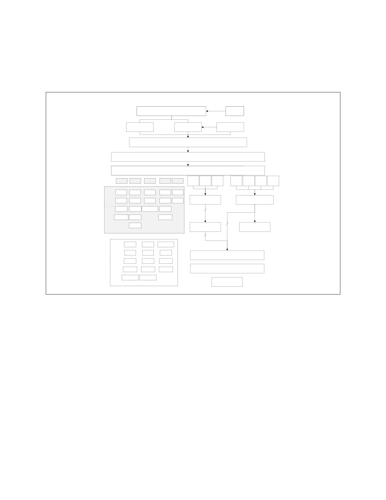
The basic pipeline functionality of the Golden Cove microarchitecture is depicted in Figure 2-1.
ITLB + 32KB Instruction Cache
BPU
MSROM
Decode
ȝ RS &DFKH
ȝRS 4XHXH
Allocate / Rename / Move Elimination / Zero Idiom
Scheduler / Reservation Station
P2
P3
P11
P4
P9
P7
P8
P0
P1
P5
P6
P10
AGU
AGU
AGU
STD
STD
AGU
AGU
ALU
ALU
ALU
ALU
ALU
LEA
LEA
LEA
LEA
LEA
Load Buffer
Store Buffer
INT
Shift
MUL
MULHi
Shift
3x256
2x256
2x512
1x512
JMP1
IDIV
JMP2
*H
LD DTLB
STA DTLB
3x256
2x512
FMA
FMA
FMA512
ALU
ALU
ALU
48KB DCU
VEC
Shift
Shift
AMX
IS'LY
Shuffle
Shuffle
1.25MB Client / 2MB Server MLC
FastADD
FastADD
SOC
Figure 2-1. Processor Core Pipeline Functionality of the Golden Cove Microarchitecture
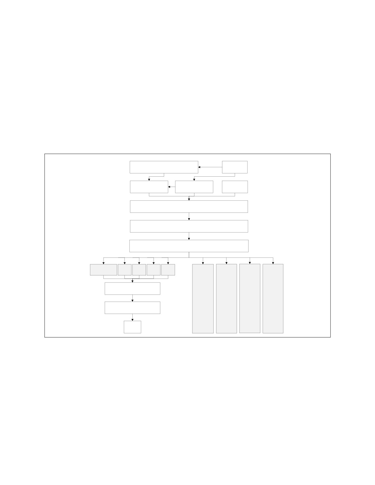
The Golden Cove front end is depicted in Figure 2-2. The front end is built to feed the wider and deeper
out-of-order core:
• Legacy decode pipeline fetch bandwidth increased from 16 to 32 bytes/cycle.
• The number of decoders increased from four to six, allowing decode of up to 6 instructions per cycle.
• The micro-op cache size increased, and its bandwidth increased to deliver up to 8 micro-ops per
cycle.
• Improved branch prediction.
Ref#: 248966-048
2-7

INTEL® 64 AND IA-32 PROCESSOR ARCHITECTURES
ITLB + 32KB Instruction Cache
BPU
MSROM
Decode
ȝ RS &DFKH
ȝRS 4XHXH
Figure 2-2. Processor Front End of the Golden Cove Microarchitecture
Improvements for large code footprint workloads:
• Double the size of the instruction TLB: 128256 entries for 4K pages, 1632 entries for 2M/4M
pages.
• Bigger branch prediction structures.
• Enhanced code prefetcher.
• Improved LSD coverage.
• The IDQ can hold 144 uops per logical processor in single thread mode, or 72 uops per thread when
SMT is active.
Additional improvements include:
• Significant increase in size of key buffer structures to enable deeper OOO execution and expose more
instruction level parallelism.
• Wider machine:
— Wider allocation (56 uops per cycle) and retirement (48 uops per cycle) width.
— Increase in number of execution ports (1012).
— Greater capabilities per execution port.
Table 2-1 summarizes the OOO engine's capability to dispatch different types of operations to ports.
Ref#: 248966-048
2-8

INTEL® 64 AND IA-32 PROCESSOR ARCHITECTURES
Table 2-1. Dispatch Port and Execution Stacks of the Golden Cove Microarchitecture
Port 0
Port 11
Port 2
Port 3
Port 4
Port 52
Port 6
Ports 7, 8
Port 9
Port 10
Port 11
INT ALU
INT
Load
Load
Store
INT ALU
INT ALU
Store
Store
INT ALU
Load
ALU3
Data
Address
Data
LEA
LEA
LEA
LEA
LEA
INT Shift
INT MUL
INT Shift
INT Mul
Hi
Jump1
Jump2
INT Div
FMA
FMA*
FMA**
Vec ALU
Fast
Fast
Adder*
Adder
Vec
Shift
Vec
Vec ALU
ALU*
FP Div
Shuffle
Vec
Shift*
Shuffle*
NOTES:
1. “*” in this table indicates that these features are not available for 512-bit vectors.
2. “**” in this table indicates that these features are not available for 512-bit vectors in Client parts.
3. The Golden Cove microarchitecture implemented performance improvements requiring constraint of the micro-ops which
use *H partial registers (i.e. AH, BH, CH, DH). See Section 3.5.2.3 for more details.
Table 2-2 lists execution units and common representative instructions that rely on these units.
Throughput improvements across the Intel® SSE, Intel AVX, and general-purpose instruction sets are
related to the number of units for the respective operations, and the varieties of instructions that execute
using a particular unit.
Table 2-2. Golden Cove Microarchitecture Execution Units and Representative Instructions1
Execution
# of Unit
Instructions
Unit
add, and, cmp, or, test, xor, movzx, movsx, mov, (v)movdqu, (v)movdqa, (v)movap*,
ALU
52
(v)movup*
SHFT
23
sal, shl, rol, adc, sarx, adcx, adox, etc.
Slow Int
1
mul, imul, bsr, rcl, shld, mulx, pdep, etc.
BM
2
andn, bextr, blsi, blsmsk, bzhi, etc.
2x256-bit
(v)add, (v)cmp. (v)max, (v)min, (v)sub, (v)cvtps2dq, (v)cvtdq2ps, (v)cvtsd2sl, (v)cvtss2sl
1x512-bit
Vec ALU
3x256-bit
(v)pand, (v)por, (v)pxor, (v)movq, (v)movq, (v)movap*, (v)movup*, (v)andp*, (v)orp*,
2x512-bit
(v)paddb/w/d/q, (v)blendv*, (v)blendp*, (v)pblendd
2x256-bit
Vec_Shft
(v)psllv*, (v)psrlv*, vector shift count in imm8
1x512-bit
VEC Add (in
2x256-bit
(v)add*, (v)cmp*, (v)max*, (v)min*, (v)sub*, (v)padds*, (v)paddus*, (v)psign, (v)pabs,
VEC FMA)
1x512-bit
(v)pavgb, (v)pcmpeq*, (v)pmax, (v)cvtps2dq, (v)cvtdq2ps, (v)cvtsd2si, (v)cvtss2si
Ref#: 248966-048
2-9

INTEL® 64 AND IA-32 PROCESSOR ARCHITECTURES
Table 2-2. Golden Cove Microarchitecture Execution Units and Representative Instructions1 (Contd.)
Execution
# of Unit
Instructions
Unit
VEC Fast
2x256-bit
(v)add*, (v)addsub*, (v)sub*
Add
1x512-bit
Shuffle
2x256-bit
(v)shufp*, vperm*, (v)pack*, (v)unpck*, (v)punpck*, (v)pshuf*, (v)pslldq, (v)alignr,
(v)pmovzx*, vbroadcast*, (v)pslldq, (v)psrldq, (v)pblendw (new cross lane shuffle on
1x512-bit
both ports)
Vec
2x256-bit
(v)mul*, (v)pmul*, (v)pmadd*
Mul/FMA
(1 or
2)x512-bit
SIMD Misc
1
STTNI, (v)pclmulqdq, (v)psadw, vector shift count in xmm
FP Mov
1
(v)movsd/ss, (v)movd gpr
DIVIDE
1
divp*, divs*, vdiv*, sqrt*, vsqrt*, rcp*, vrcp*, rsqrt*, idiv
NOTES:
1. Execution unit mapping to MMX instructions are not covered in this table. See Section 15.16.5 on MMX instruction
throughput remedy.
2. The Golden Cove microarchitecture implemented performance improvements requiring constraint of the micro-ops which
use *H partial registers (i.e. AH, BH, CH, DH). See Section 3.5.2.3 for more details.
3. Ibid.
Table 2-3 describes bypass delay in cycles between producer and consumer operations.
Table 2-3. Bypass Delay Between Producer and Consumer Micro-Ops
TO [EU/PORT/Latency]
SHUF/
FROM
Fast
SIMD/0,1/1
FMA/0,1/4
MUL/0,1/4
SIMD/5/1,3
1,5/1,
V2I/0/3
[EU/Port/Latency]
Adder/1,5/3
3
SIMD/0,1/1
0
1
1
1
0
0
0
FMA/0,1/4
1
0
1
0
0
0
0
MUL/0,1/4
1
0
1
0
0
0
0
Fast Adder/0,1/3
1
0
1
-1
0
0
0
SIMD/5/1,3
0
1
1
1
0
0
0
SHUF/1,5/1,3
0
0
1
0
0
0
0
V2I/0/3
0
0
1
0
0
0
0
I2V/5/1
0
1
1
0
0
0
0
The attributes that are relevant to the producer/consumer micro-ops for bypass are a triplet of
abbreviation/one or more port number/latency cycle of the uop. For example:
•
“SIMD/0,1/1” applies to a 1-cycle vector SIMD uop dispatched to either port 0 or port 1.
•
“SIMD/5/1,3” applies to either a 1-cycle or 3-cycle non-shuffle uop dispatched to port 5.
•
“V2I/0/3” applies to a 3-cycle vector-to-integer uop dispatched to port 0.
Ref#: 248966-048
2-10

INTEL® 64 AND IA-32 PROCESSOR ARCHITECTURES
•
“I2V/5/1” applies to a 1-cycle integer-to-vector uop dispatched to port 5.
•
“Fast Adder/1,5/3” applies to either a 3-cycle 256-bit uop dispatched to either port 1 or port 5, or a
512-bit uop dispatched to port 5. This operation supports two cycles back-to-back between a pair of
Fast Adder operations.
A new Fast Adder1 unit is added as 512-bit on port 5 in VEC stack, and as 256-bit on ports 1 and 5. The
Fast Adder performs floating-point ADD/SUB operations in 3 cycles.
Back-to-back ADD/SUB operations that are both executed on the Fast Adder unit perform the operations
in two cycles.
• In 128/256-bit, back-to-back ADD/SUB operations executed on the Fast Adder unit perform the
operations in two cycles.
• In 512-bit, back-to-back ADD/SUB operations are executed in two cycles if both operations use the
Fast Adder unit on port 5.
The following instructions are executed by the Fast Adder unit:
•
(V)ADDSUBSS/SD/PS/PD
•
(V)ADDSS/SD/PS/PD
•
(V)SUBSS/SD/PS/PD
2.3.1.1
Cache Subsystem and Memory Subsystem
The cache subsystem and memory subsystem changes in the Golden Cove microarchitecture are:
• Maximum load bandwidth increased from 2 to 3 loads per cycle. Bandwidth of Intel AVX-512 loads,
Intel AMX loads, and MMX/x87 loads remain at a maximum of 2 loads per cycle.
• Simultaneous handling of more loads and stores enabled by enlarged buffers.
• Number of entries for 4K pages in the load DTLB increased from 64 to 96.
• Page Miss handler can handle up to four D-side page walks in parallel instead of two.
• Increased number of outstanding DCU and MLC misses.
• Enhanced data prefetchers for increased memory parallelism.
• Partial store forwarding allowing forwarding data from store to load also when only part of the load
was covered by the store (in case the load's offset matches the store's offset).
2.3.1.2
Avoiding Destination False Dependency
Some SIMD instructions incur false dependency on the destination operand. The following instructions
are affected:
• VFMULCSH, VFMULCPH
• VFCMULCSH, VFCMULCPH
• VPERMD, VPERMQ, VPERMPS, VPERMPD
• VRANGE[SS,PS,SD,PD]
• VGETMANTSH, VGETMANTSS, VGETMANTSD
• VGETMANTPS, VGETMANTPD (memory versions only)
• VPMULLQ
1. The Fast Adder unit is not available on 512-bit vectors in Client parts.
Ref#: 248966-048
2-11

INTEL® 64 AND IA-32 PROCESSOR ARCHITECTURES
Recommendation: Use dependency breaking zero idioms on the destination register before the
affected instructions to avoid potential slowdown from the false dependency.
Example 2-5. Breaking False Dependency through Zero Idiom
Code with False Dependency Impact
Mitigation: Break False Dependency with Zero Idiom
vaddps zmm3, zmm4, zmm5
vaddps zmm3, zmm4, zmm5
vmovaps [rsi], zmm3
vmovaps [rsi], zmm3
vfmulcph zmm3, zmm2, zmm1
;False dependency on
vpxord zmm3, zmm3, zmm3
;Dependency-breaking
zmm3.
zero idiom.
Will not execute out-of-order
vfmulcph zmm3, zmm2, zmm1
;Execute out-of-order
until vaddps writes zmm3.
without waiting for
vaddps result.
Ref#: 248966-048
2-12
INTEL® 64 AND IA-32 PROCESSOR ARCHITECTURES
2.4
ICE LAKE CLIENT MICROARCHITECTURE
The Ice Lake client microarchitecture introduces the following new features that allow optimizations of
applications for performance and power consumption:
• Targeted vector acceleration.
• Crypto acceleration.
• Intel® Software Guard Extensions (Intel® SGX) enhancements.
• Cache line writeback instruction (CLWB).
2.4.1
Ice Lake Client Microarchitecture Overview
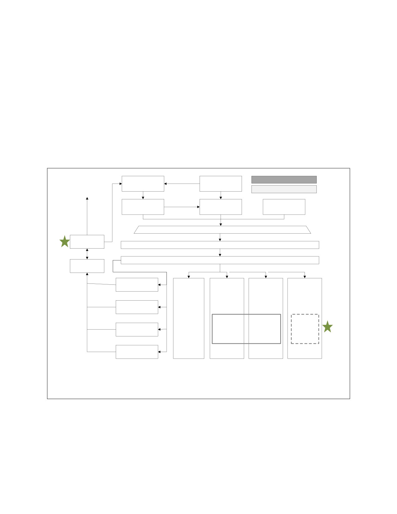
The Ice Lake client microarchitecture builds on the successes of the Skylake client microarchitecture.
The basic pipeline functionality of the Ice Lake Client microarchitecture is depicted in Figure 2-3.
.% ,QVWUXFWLRQ &DFKH
BPU
/HJDF\ 'HFRGH
ȝ RS &DFKH
06520
3LSHOLQH
ȝRS 4XHXH
$OORFDWH
5HQDPH
0RYH (OLPLQDWLRQ
=HUR ,GLRP
6FKHGXOHU
5HVHUYDWLRQ 6WDWLRQ
3
3
3
3
3
3
Port 0
Port 1
Port 5
Port 6
6WRUH 'DWD
/RDG
67'
/RDG
67$
$/8
$/8
$/8
$/8
/($
/($
/($
/($
,17
.% / 'DWD &DFKH
6KLIW
08/
08/+L
6KLIW
-03
,',9
*H
-03
*H
.% / 'DWD &DFKH
)0$
)0$
$/8
$/8
$/8
9(&
6KLIW
6KLIW
62&
IS',9
6KXIIOH
6KXIIOH
Figure 2-3. Processor Core Pipeline Functionality of the Ice Lake Client Microarchitecture1
NOTES:
1.
“*” in the figure above indicates these features are not available for 512-bit vectors.
2. “INT” represents GPR scalar instructions.
3. “VEC” represents floating-point and integer vector instructions.
4. “MULHi” produces the upper 64 bits of the result of an iMul operation that multiplies two 64-bit registers and places the
result into two 64-bits registers.
5. The “Shuffle” on port 1 is new, and supports only in-lane shuffles that operate within the same 128-bit sub-vector.
6. The “IDIV” unit on port 1 is new, and performs integer divide operations at a reduced latency.
7. The Golden Cove microarchitecture implemented performance improvements requiring constraint of the micro-ops which
use *H partial registers (i.e. AH, BH, CH, DH). See Section 3.5.2.3 for more details.
Ref#: 248966-048
2-13
INTEL® 64 AND IA-32 PROCESSOR ARCHITECTURES
The Ice Lake client microarchitecture introduces the following new features:
• Significant increase in size of key structures enable deeper OOO execution.
• Wider machine: 4 5 wide allocation, 8 10 execution ports.
• Intel AVX-512 (new for client processors): 512-bit vector operations, 512-bit loads and stores to
memory, and 32 new 512-bit registers.
• Greater capabilities per execution port (e.g., SIMD shuffle, LEA), reduced latency Integer Divider.
•
2×BW for AES-NI peak throughput for existing binaries (microarchitectural).
• Rep move string acceleration.
•
50% increase in size of the L1 data cache.
• Reduced effective load latency.
•
2×L1 store bandwidth: 1 2 stores per cycle.
• Enhanced data prefetchers for increased memory parallelism.
• Larger 2nd level TLB.
• Larger uop cache.
• Improved branch predictor.
• Large page ITLB size in single thread mode doubled.
• Larger L2 cache.
The Ice Lake client microarchitecture supports flexible integration of multiple processor cores with a
shared uncore sub-system consisting of a number of components including a ring interconnect to
multiple slices of L3, processor graphics, integrated memory controller, interconnect fabrics, and more.
2.4.1.1
The Front End
The front end changes in Ice Lake Client microarchitecture include:
• Improved branch predictor.
• Large page ITLB in single thread mode increased from 8 to 16 entries.
• Larger uop cache.
• The IDQ can hold 70 uops per logical processor vs. 64 uops per logical processor in previous
generations when two sibling logical processors in the same core are active (2×70 vs. 2×64 per
core). If only one logical processor is active in the core, the IDQ can hold 70 uops vs. 64 uops.
• The LSD in the IDQ can detect loops of up to 70 uops per logical processor irrespective single thread
or multi thread operation.
Ref#: 248966-048
2-14

INTEL® 64 AND IA-32 PROCESSOR ARCHITECTURES
2.4.1.2
The Out of Order and Execution Engines
The Out of Order and execution engines changes in Ice Lake client microarchitecture include:
• A significant increase in size of reorder buffer, load buffer, store buffer, and reservation stations
enable deeper OOO execution and higher cache bandwidth.
• Wider machine: 4 5 wide allocation, 8 10 execution ports.
• Greater capabilities per execution port (e.g., SIMD shuffle, LEA).
• Reduced latency Integer Divider.
• A new iDIV unit was added that significantly reduces the latency and improves the of throughput of
integer divide operations.
Table 2-4 summarizes the OOO engine's capability to dispatch different types of operations to ports.
Table 2-4. Dispatch Port and Execution Stacks of the Ice Lake Client Microarchitecture
Port 0
Port 11
Port 2
Port 3
Port 4
Port 5
Port 6
Port 7
Port 8
Port 9
INT ALU
INT ALU
Load
Load
Store
INT ALU
INT ALU
Store
Store
Store
Data
Address
Address
Data
LEA
LEA
LEA
LEA
INT Shift
INT Mul
INT MUL
INT Shift
Hi
Jump1
INT Div
Jump2
FMA
FMA*
Vec ALU
Vec ALU
Vec ALU*
Vec
Shuffle
Vec Shift
Vec
Shift*
FP Div
Vec
Shuffle*
NOTES:
1. “*” in this table indicates these features are not available for 512-bit vectors.
Table 2-5 lists execution units and common representative instructions that rely on these units.
Throughput improvements across the Intel SSE, Intel AVX, and general-purpose instruction sets are
related to the number of units for the respective operations, and the varieties of instructions that execute
using a particular unit.
Table 2-5. Ice Lake Client Microarchitecture Execution Units and Representative Instructions1
Execution
# of
Instructions
Unit
Unit
ALU
4
add, and, cmp, or, test, xor, movzx, movsx, mov, (v)movdqu, (v)movdqa, (v)movap*, (v)movup*
SHFT
2
sal, shl, rol, adc, sarx, adcx, adox, etc.
Slow Int
1
mul, imul, bsr, rcl, shld, mulx, pdep, etc.
BM
2
andn, bextr, blsi, blsmsk, bzhi, etc.
Vec ALU
3
(v)pand, (v)por, (v)pxor, (v)movq, (v)movq, (v)movap*, (v)movup*, (v)andp*, (v)orp*,
(v)paddb/w/d/q, (v)blendv*, (v)blendp*, (v)pblendd
Vec_Shft
2
(v)psllv*, (v)psrlv*, vector shift count in imm8
Vec Add
2
(v)addp*, (v)cmpp*, (v)max*, (v)min*, (v)padds*, (v)paddus*, (v)psign, (v)pabs, (v)pavgb,
(v)pcmpeq*, (v)pmax, (v)cvtps2dq, (v)cvtdq2ps, (v)cvtsd2si, (v)cvtss2si
Ref#: 248966-048
2-15

INTEL® 64 AND IA-32 PROCESSOR ARCHITECTURES
Table 2-5. Ice Lake Client Microarchitecture Execution Units and Representative Instructions1
Execution
# of
Instructions
Unit
Unit
Shuffle
2
(v)shufp*, vperm*, (v)pack*, (v)unpck*, (v)punpck*, (v)pshuf*, (v)pslldq, (v)alignr, (v)pmovzx*,
vbroadcast*, (v)pslldq, (v)psrldq, (v)pblendw
Vec Mul
2
(v)mul*, (v)pmul*, (v)pmadd*
SIMD Misc
1
STTNI, (v)pclmulqdq, (v)psadw, vector shift count in xmm
FP Mov
1
(v)movsd/ss, (v)movd gpr
DIVIDE
1
divp*, divs*, vdiv*, sqrt*, vsqrt*, rcp*, vrcp*, rsqrt*, idiv
NOTES:
1. Execution unit mapping to MMX instructions are not covered in this table. See Section 15.16.5 on MMX instruction
throughput remedy.
Table 2-6 describes bypass delay in cycles between producer and consumer operations.
Table 2-6. Bypass Delay Between Producer and Consumer Micro-ops
TO [EU/PORT/Latency]
FROM
SIMD/0,1/1
FMA/0,1/4
VIMUL/0,1/4
SIMD/5/1,3
SHUF/5/1,
V2I/0/3
I2V/5/1
[EU/Port/Latency]
3
SIMD/0,1/1
0
1
1
0
0
0
NA
FMA/0,1/4
1
0
1
0
0
0
NA
VIMUL/0,1/4
1
0
1
0
0
0
NA
SIMD/5/1,3
0
1
1
0
0
0
NA
SHUF/5/1,3
0
0
1
0
0
0
NA
V2I/0/3
0
0
1
0
0
0
NA
I2V/5/1
0
1
1
0
0
0
NA
The attributes that are relevant to the producer/consumer micro-ops for bypass are a triplet of abbrevi-
ation/one or more port number/latency cycle of the uop. For example:
•
“SIMD/0,1/1” applies to 1-cycle vector SIMD uop dispatched to either port 0 or port 1.
•
“SIMD/5/1,3” applies to either a 1-cycle or 3-cycle non-shuffle uop dispatched to port 5.
•
“V2I/0/3” applies to a 3-cycle vector-to-integer uop dispatched to port 0.
•
“I2V/5/1” applies to a 1-cycle integer-to-vector uop to port 5.
Ref#: 248966-048
2-16

INTEL® 64 AND IA-32 PROCESSOR ARCHITECTURES
2.4.1.3
Cache and Memory Subsystem
The cache hierarchy changes in Ice Lake Client microarchitecture include:
•
50% increase in size of the L1 data cache.
•
2×L1 store bandwidth: 3 4 AGUs, 1 2 store data.
• Simultaneous handling of more loads and stores enabled by enlarged buffers.
• Higher cache bandwidth compared to previous generations.
• Larger 2nd level TLB: 1.5K entries 2K entries.
• Enhanced data prefetchers for increased memory parallelism.
• L2 cache size increased from 256KB to 512KB.
• L2 cache associativity increased from 4 ways to 8 ways.
• Significant reduction in effective load latency.
Table 2-7. Cache Parameters of the Ice Lake Client Microarchitecture
Capacity /
Line Size
Latency1
Peak Bandwidth
Sustained Bandwidth
Update
Level
Associativity
(bytes)
(cycles)
(bytes/cycles)
(bytes/cycles)
Policy
First Level
48KB/8
64
5
2×64B loads + 1x64B
Same as peak
Writeback
(DCU)
or 2x32B stores
Second
512KB/8
64
13
64
48
Writeback
Level (MLC)
Third Level
Up to 2MB per
64
xx2
32
21
Writeback
(LLC)
core/up to 16 ways
NOTES:
1. Software-visible latency/bandwidth will vary depending on access patterns and other factors.
2. This number depends on core count.
The TLB hierarchy consists of dedicated level one TLB for instruction cache, TLB for L1D, shared L2 TLB
for 4K and 4MB pages and a dedicated L2 TLB for 1GB pages.
Table 2-8. TLB Parameters of the Ice Lake Client Microarchitecture
Per-thread Entries
Level
Page Size
Entries ST
MT Latency
Associativity
Instruction
4KB
128
64
8
Instruction
2MB/4MB
16
8
8
First Level Data (loads)
4KB
64
64 competitively
4
shared
First Level Data (loads)
2MB/4MB
32
32 competitively
4
shared
First Level Data (loads)
1GB
8
8 competitively shared
8
First Level Data (stores)
Shared for all page
16
16 competitively
16
sizes
shared
Second Level
Shared for all page
20481
2048 competitively
16
sizes
shared
NOTES:
1. 4K pages can use all 2048 entries. 2/4MB pages can use 1024 entries (in 8 ways), sharing them with 4K pages. 1GB
pages can use the other 1024 entries (in 8 ways), also sharing them with 4K pages.
Ref#: 248966-048
2-17

INTEL® 64 AND IA-32 PROCESSOR ARCHITECTURES
Paired Stores
Ice Lake Client microarchitecture includes two store pipelines in the core, with the following features:
• Two dedicated AGU for LDs on ports 2 and 3.
• Two dedicated AGU for STAs on ports 7 and 8.
• Two fully featured STA pipelines.
• Two 256-bit wide STD pipelines (Intel AVX-512 store data takes two cycles to write).
• Second senior store pipeline to the DCU via store merging.
Ice Lake Client microarchitecture can write two senior stores to the cache in a single cycle if these two
stores can be paired together. That is:
• The stores must be to the same cache line.
• Both stores are of the same memory type, WB or USWC.
• None of the stores cross cache line or page boundary.
In order to maximize performance from the second store port try to:
• Align store operations whenever possible.
• Place consecutive stores in the same cache line (not necessarily as adjacent instructions).
As seen in Example 2-6, it is important to take into consideration all stores, explicit or not.
Example 2-6. Considering Stores
Stores are Paired Across Loop Iterations
Stores Not Paired Due to Stack Update in Between
Loop:
Loop:
compute reg
call function to compute reg
…
…
store [X], reg
store [X], reg
add X, 4
add X, 4
jmp Loop
; stores from different iterations of the
jmp Loop
; stores from different iterations of the
loop can be paired all together because
loop cannot be paired anymore because
they usually would be same line
of the call store to stack
; the call is disturbing pairing
Ref#: 248966-048
2-18

INTEL® 64 AND IA-32 PROCESSOR ARCHITECTURES
In some cases it is possible to rearrange the code to achieve store pairing. Example 2-7 provides details.
Example 2-7. Rearranging Code to Achieve Store Pairing
Stores to Different Cache Lines - Not Paired
Unrolling May Solve the Problem
Loop:
Loop:
... compute ymm1 …
... compute ymm1 …
vmovaps [x], ymm1
vmovaps [x], ymm1
... compute ymm2 …
... compute new ymm1 …
vmovaps [y], ymm2
vmovaps [x+32], ymm1
add x, 32
... compute ymm2 …
add y, 32
vmovaps [y], ymm2
jmp Loop
; this loop cannot pair any store because
... compute new ymm2 …
of alternating store to different cache
vmovaps [y+32], ymm2
lines [x] and [y]
add x, 64
add y, 64
jmp Loop
; the loop was unrolled 2 times and stores
re-arranged to make sure two stores to
the same cache line are placed one after
another. Now stores to addresses [x] and
[x+32] are to the same cache line and
could be paired together and executed in
same cycle
2.4.1.4
New Instructions
New instructions and architectural changes in Ice Lake Client microarchitecture are listed below. Actual
support may be product dependent.
•
Crypto acceleration
— SHA NI for acceleration of SHA1 and SHA256 hash algorithms.
— Big-Number Arithmetic (IFMA): VPMADD52 - two new instructions for big number multiplication
for acceleration of RSA vectorized SW and other Crypto algorithms (Public key) performance.
— Galois Field New Instructions (GFNI) for acceleration of various encryption algorithms, error
correction algorithms, and bit matrix multiplications.
— Vector AES and Vector Carry-less Multiply (PCLMULQDQ) instructions to accelerate AES and
AES-GCM.
•
Security Technologies
— Intel® SGX enhancements to improve usability and applicability: EDMM, multi-package server
support, support for VMM memory oversubscription, performance, larger secure memory.
•
Sub Page protection for better performance of security VMMs.
•
Targeted Acceleration
— Vector Bit Manipulation Instructions: VBMI1 (permutes, shifts) and VBMI2 (Expand, Compress,
Shifts)- used for columnar database access, dictionary based decompression, discrete mathe-
matics, and data-mining routines (bit permutation and bit-matrix-multiplication).
— VNNI with support for integer 8 and 16 bits data types- CNN/ML/DL acceleration.
— Bit Algebra (POPCNT, Bit Shuffle).
— Cache line writeback instruction (CLWB) enables fast cache-line update to memory, while
retaining clean copy in cache.
•
Platform analysis features for more efficient performance software tuning and debug.
— AnyThread removal.
Ref#: 248966-048
2-19

INTEL® 64 AND IA-32 PROCESSOR ARCHITECTURES
— 2x general counters (up to 8 per-thread).
— Fixed Counter 3 for issue slots.
— New performance metrics for built-in support for Level 1 Top-Down method (% of Issue slots that
are front-end bound, back-end bound, bad speculation, retiring) while leaving the 8 general
purpose counters free for software use.
2.4.1.5
Ice Lake Client Microarchitecture Power Management
Processors based on Ice Lake client microarchitecture are the first client processors whose cores may
execute at a different frequency from one another. The frequency is selected based on the specific
instruction mix; the type, width and number of vector instructions of the program that executes on each
core, the ratio between active time and idle time of each core, and other considerations such as how
many cores share similar characteristics.
Most of the power management features of Skylake Server Microarchitecture (see Section 2.5) is appli-
cable to Ice Lake Client microarchitecture as well. The main differences are the following:
• The typical P0n max frequency difference between Intel® Advanced Vector Extensions (Intel®
AVX-512) and Intel® Advanced Vector Extensions 2 (Intel® AVX2) on Ice Lake Client microarchi-
tecture is much lower than on Skylake Server microarchitecture. Therefore, the negative impact on
overall application performance is much smaller.
• All processors based on Ice Lake Client microarchitecture contain a single 512-bit FMA unit, whereas
some of the processors based on Skylake Server microarchitecture contain two such units. Both
processors contain two 256-bit FMA units. The power consumed by Ice Lake Client FMA units is the
same, whereas on Skylake Server the 512-bit units consume twice as much.
Compute heavy workloads, especially those that span multiple Ice Lake client cores, execute at a lower
frequency than P0n, both under Intel AVX-512 and under Intel AVX2 instruction sets, due to power
limitations. In this scenario, Intel AVX-512 architecture, which requires less dynamic instructions to
complete the same task than Intel AVX2 architecture, consumes less power and thus may achieve higher
frequency. The net result may be higher performance due to the shorter path length and a bit higher
frequency.
There are still some cases where coding to the Intel AVX-512 instruction set yields lower performance
than when coding to the Intel AVX2 instruction set. Sometimes it is due to microarchitecture artifacts of
longer vectors, in other cases the natural vectors are just not long enough. Most compilers are still
maturing their Intel AVX-512 support, and it may take them a few more years to generate optimal code.
The general recommendation in the Skylake Server Power Management section (see Section 2.5.3) still
holds. Developers should code to the Intel AVX-512 instruction set and compare the performance to their
Intel AVX2 workload on Ice Lake client microarchitecture, before making the decision to proceed with a
complete port.
2.5
SKYLAKE SERVER MICROARCHITECTURE
The Intel® Xeon® Processor scalable processor family is based on the Skylake Server microarchitecture.
Processors based on the Skylake microarchitecture can be identified using CPUID’s DisplayFamily_Dis-
playModel signature, which can be found in Table 2-1 of CHAPTER 2 of Intel® 64 and IA-32 Architectures
Software Developer’s Manual, Volume 4.
The Skylake Server microarchitecture introduces the following new features1 that allow you to optimize
your application for performance and power consumption.
• A new core based on the Skylake Server microarchitecture with process improvements based on the
Kaby Lake microarchitecture.
• Intel AVX-512 support.
• More cores per socket (max 28 vs. max 22).
1. Some features may not be available on all products.
Ref#: 248966-048
2-20
INTEL® 64 AND IA-32 PROCESSOR ARCHITECTURES
•
6 memory channels per socket in Skylake microarchitecture vs. 4 in the Broadwell microarchitecture.
• Bigger L2 cache, smaller non inclusive L3 cache.
• Intel® Optane™ support.
• Intel® Omni-Path Architecture (Intel® OPA).
• Sub-NUMA Clustering (SNC) support.
The green stars in Figure 2-4 represent new features in Skylake Server microarchitecture compared to
Skylake microarchitecture for client; a 1MB L2 cache and an additional Intel AVX-512 FMA unit on port 5
which is available on some parts.
Since port 0 and port 1 are 256-bits wide, Intel AVX-512 operations that will be dispatched to port 0 will
execute on both port 0 and port 1; however, other operations such as lea can still execute on port 1 in
parallel. See the red block in Figure 2-8 for the fusion of ports 0 and 1.
Notice that, unlike Skylake microarchitecture for client, the Skylake Server microarchitecture has its
front end loop stream detector (LSD) disabled.
32K
AVX-512 Port Fusion
BPU
Instruction Cache
Dedicated AVX-512 unit
uncore
Legacy Decode
Decoded
MSROM
Pipeline
ICache
Micro-Op Queue
1M L2 Cache
Allocate/Rename/Retire/Move Elimination/Zero Idiom
Scheduler
32K Data
Cache
Port 2 LD/STA
Port 6
Port 0
Port 1
Port 5
INTEGER ALU
INTEGER ALU
INTEGER ALU
INTEGER ALU
INTEGER
DIVIDE
INTEGER MUL
FAST LEA
SHIFT
BRANCH 2
SLOW LEA
VEC SHUFFLE
Port 3 LD/STA
BRANCH 1
FAST LEA
VEC FMA
VEC FMA
VEC FMA
VEC MUL
VEC MUL
VEC MUL
Port 4 STD
VEC ADD
VEC ADD
VEC ADD
VEC ALU
VEC ALU
VEC ALU
VEC SHIFTER
VEC SHIFTER
Port 7 STA
INTEGER represent GPR scalar instructions.
VEC represent floating point and integer vector instructions.
SLOW LEA represent a lea with two registers and displacement, all other lea
versions considered as FAST LEA
BRANCH1 is primary branch and more capable than BRANCH2
Figure 2-4. Processor Core Pipeline Functionality of the Skylake Server Microarchitecture
Ref#: 248966-048
2-21

INTEL® 64 AND IA-32 PROCESSOR ARCHITECTURES
2.5.1
Skylake Server Microarchitecture Cache
Intel Xeon scalable processors based on Skylake server microarchitecture has significant changes in core
and uncore architecture to improve performance and scalability of several components compared with
the previous generation of the Intel Xeon processors based on the Broadwell microarchitecture.
2.5.1.1
Larger Mid-Level Cache
Skylake server microarchitecture implements a mid-level (L2) cache of 1 MB capacity with a minimum
load-to-use latency of 14 cycles. The mid-level cache capacity is four times larger than the capacity in
previous Intel Xeon processor family implementations. The line size of the mid-level cache is 64B and it
is 16-way associative. The mid-level cache is private to each core.
Software that has been optimized to place data in mid-level cache may have to be revised to take advan-
tage of the larger mid-level cache available in Skylake server microarchitecture.
2.5.1.2
Non-Inclusive Last Level Cache
The last level cache (LLC) in Skylake is a non-inclusive, distributed, shared cache. The size of each of the
banks of last level cache has shrunk to 1.375 MB per bank. Because of the non-inclusive nature of the last
level cache, blocks that are present in the mid-level cache of one of the cores may not have a copy resi-
dent in a bank of last level cache. Based on the access pattern, size of the code and data accessed, and
sharing behavior between cores for a cache block, the last level cache may appear as a victim cache of
the mid-level cache and the aggregate cache capacity per core may appear to be a combination of the
private mid-level cache per core and a portion of the last level cache.
2.5.1.3
Skylake Server Microarchitecture Cache Recommendations
A high-level comparison between Skylake server microarchitecture cache and the previous generation
Broadwell microarchitecture cache is available in the table below.
Table 2-9. Cache Comparison Between Skylake Microarchitecture and Broadwell Microarchitecture
Cache level
Category
Broadwell
Skylake Server
Microarchitecture
Microarchitecture
L1 Data Cache
Size [KB]
32
32
Unit (DCU)
Latency [cycles]
4-6
4-6
Max bandwidth [bytes/cycles]
96
192
Sustained bandwidth [bytes/cycles]
93
133
Associativity [ways]
8
8
L2 Mid-level Cache
Size [KB]
256
1024 (1MB)
(MLC)
Latency [cycles]
12
14
Max bandwidth [bytes/cycles]
32
64
Sustained bandwidth [bytes/cycles]
25
52
Associativity [ways]
8
16
Ref#: 248966-048
2-22
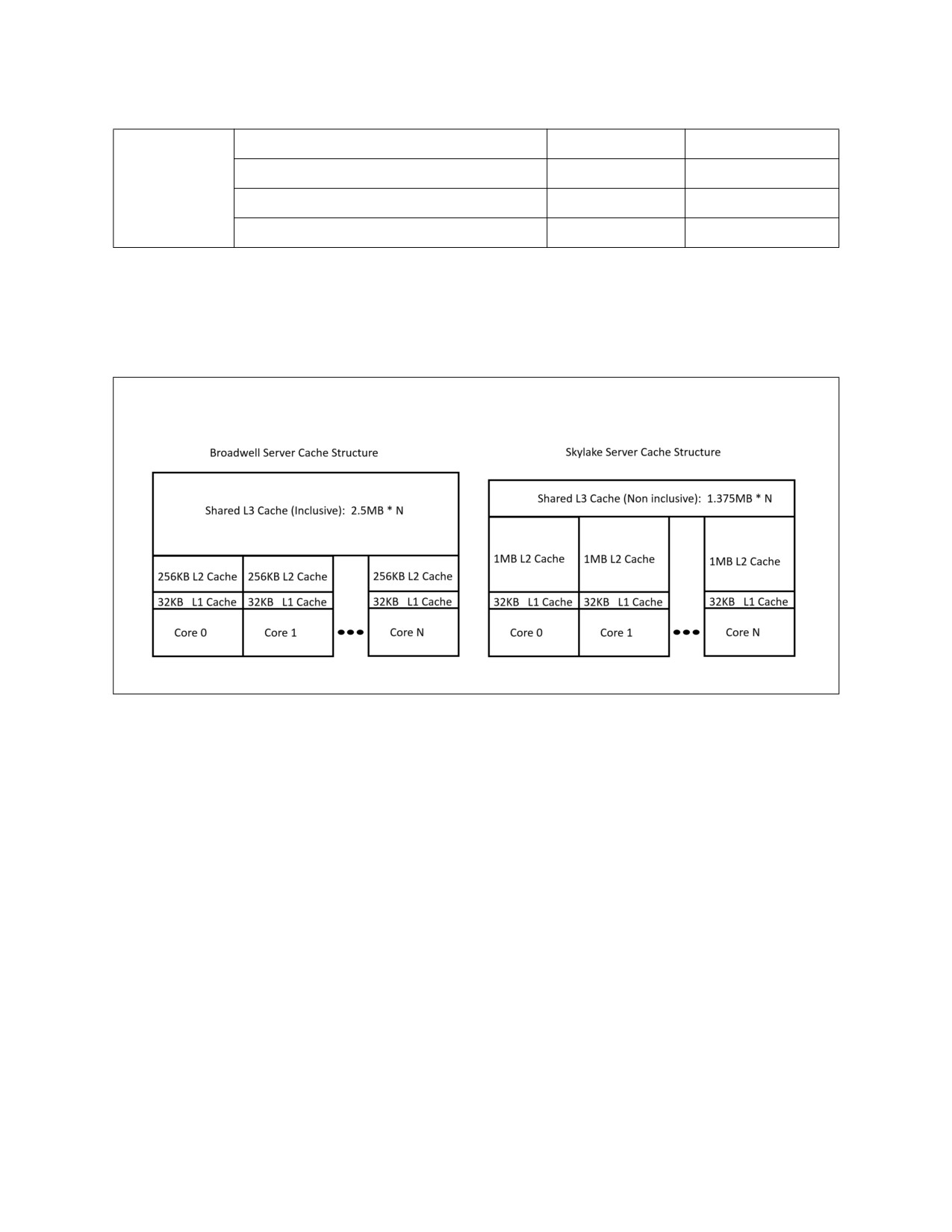
INTEL® 64 AND IA-32 PROCESSOR ARCHITECTURES
Table 2-9. Cache Comparison Between Skylake Microarchitecture and Broadwell Microarchitecture
L3 Last-level
Size [MB]
Up to 2.5 per core
up to 1.3751 per core
Cache (LLC)
Latency [cycles]
50-60
50-70
Max bandwidth [bytes/cycles]
16
32
Sustained bandwidth [bytes/cycles]
14
15
NOTES:
1. Some Skylake server parts have some cores disabled and hence have more than 1.375 MB per core of L3 cache.
The figure below shows how Skylake server microarchitecture shifts the memory balance from
shared-distributed with high latency, to private-local with low latency.
Figure 2-5. Broadwell Microarchitecture and Skylake Server Microarchitecture Cache Structures
The potential performance benefit from the cache changes is high, but software will need to adapt its
memory tiling strategy to be optimal for the new cache sizes.
Recommendation: Rebalance application shared and private data sizes to match the smaller,
non-inclusive L3 cache, and larger L2 cache.
Choice of cache blocking should be based on application bandwidth requirements and changes from one
application to another. Having four times the L2 cache size and twice the L2 cache bandwidth compared
to the previous generation Broadwell microarchitecture enables some applications to block to L2 instead
of L1 and thereby improves performance.
Recommendation: Consider blocking to L2 on Skylake Server microarchitecture if L2 can sustain the
application’s bandwidth requirements.
The change from inclusive last level cache to non-inclusive means that the capacity of mid-level and last
level cache can now be added together. Programs that determine cache capacity per core at run time
should now use a combination of mid-level cache size and last level cache size per core to estimate the
effective cache size per core. Using just the last level cache size per core may result in non-optimal use
of available on-chip cache; see Section 2.5.2 for details.
Recommendation: In case of no data sharing, applications should consider cache capacity per core as
L2 and L3 cache sizes and not only L3 cache size.
Ref#: 248966-048
2-23

INTEL® 64 AND IA-32 PROCESSOR ARCHITECTURES
2.5.2
Non-Temporal Stores on Skylake Server Microarchitecture
Because of the change in the size of each bank of last level cache on Skylake server microarchitecture, if
an application, library, or driver only considers the last level cache to determine the size of on-chip
cache-per-core, it may see a reduction with Skylake server microarchitecture and may use non-temporal
store with smaller blocks of memory writes. Since non-temporal stores evict cache lines back to memory,
this may result in an increase in the number of subsequent cache misses and memory bandwidth
demands on Skylake Server microarchitecture, compared to the previous Intel Xeon processor family.
Also, because of a change in the handling of accesses resulting from non-temporal stores by Skylake
Server microarchitecture, the resources within each core remain busy for a longer duration compared to
similar accesses on the previous Intel Xeon processor family. As a result, if a series of such instructions
are executed, there is a potential that the processor may run out of resources and stall, thus limiting the
memory write bandwidth from each core.
The increase in cache misses due to overuse of non-temporal stores and the limit on the memory write
bandwidth per core for non-temporal stores may result in reduced performance for some applications.
To avoid the performance condition described above with Skylake server microarchitecture, include
mid-level cache capacity per core in addition to the last level cache per core for applications, libraries, or
drivers that determine the on-chip cache available with each core. Doing so optimizes the available
on-chip cache capacity on Skylake server microarchitecture as intended, with its non-inclusive last level
cache implementation.
2.5.3
Skylake Server Power Management
This section describes the interaction of Skylake Server's Power Management and its Vector ISA.
Skylake Server microarchitecture dynamically selects the frequency at which each of its cores executes.
The selected frequency depends on the instruction mix; the type, width, and number of vector instruc-
tions that execute over a given period of time. The processor also takes into account the number of cores
that share similar characteristics.
Intel® Xeon® processors based on Broadwell microarchitecture work similarly, but to a lesser extent
since they only support 256-bit vector instructions. Skylake Server microarchitecture supports Intel®
AVX-512 instructions, which can potentially draw more current and more power than Intel® AVX2
instructions.
The processor dynamically adjusts its maximum frequency to higher or lower levels as necessary, there-
fore a program might be limited to different maximum frequencies during its execution.
Table 2-10 includes information about the maximum Intel® Turbo Boost technology core frequency for
each type of instruction executed. The maximum frequency (P0n) is an array of frequencies which
depend on the number of cores within the category. The more cores belonging to a category at any given
time, the lower the maximum frequency.
Table 2-10. Maximum Intel® Turbo Boost Technology Core Frequency Levels
Level
Category
Frequency Level
Max Frequency (P0n)
Instruction Types
0
Intel® AVX2 light
Highest
Max
Scalar, AVX128, SSE, Intel® AVX2 w/o FP
instructions
or INT MUL/FMA
1
Intel® AVX2 heavy
Medium
Max Intel® AVX2
Intel® AVX2 FP + INT MUL/FMA, Intel®
instructions +
AVX-512 without FP or INT MUL/FMA
Intel® AVX-512
light instructions
2
Intel® AVX-512
Lowest
Max Intel® AVX-512
Intel® AVX-512 FP + INT MUL/FMA
heavy instructions
For per SKU max frequency details (reference figure 1-15), refer to the Intel® Xeon® Scalable Processor
Family Technical Resources page.
Ref#: 248966-048
2-24
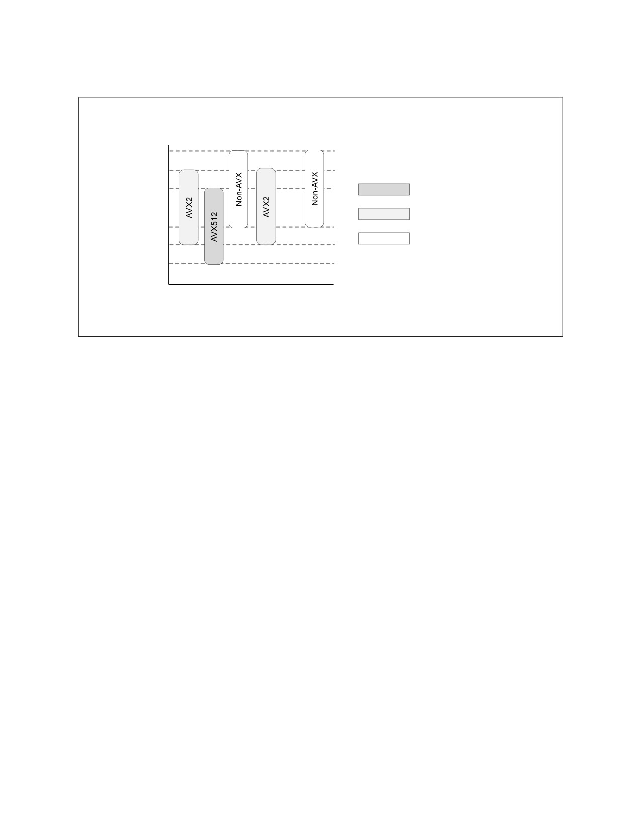
INTEL® 64 AND IA-32 PROCESSOR ARCHITECTURES
Figure 2-6 is an example for core frequency range in a given system where each core frequency is deter-
mined independently based on the demand of the workload.
P0n
P0n-AVX2
P0n-AVX-512
AVX512
Cores using Intel®AVX-512
AVX2
Cores using Intel® AVX2
P1
Non-AVX
Cores not using Intel®AVX
P1-AVX2
P1-AVX-512
Cores
Figure 2-6. Mixed Workloads
The following performance monitoring events can be used to determine how many cycles were spent in
each of the three frequency levels.
• CORE_POWER.LVL0_TURBO_LICENSE: Core cycles where the core was running in a manner where
the maximum frequency was P0n.
• CORE_POWER.LVL1_TURBO_LICENSE: Core cycles where the core was running in a manner where
the maximum frequency was P0n-AVX2.
• CORE_POWER.LVL2_TURBO_LICENSE: Core cycles where the core was running in a manner where
the maximum frequency was P0n-AVX-512.
When the core requests a higher license level than its current one, it takes the PCU up to 500
micro-seconds to grant the new license. Until then the core operates at a lower peak capability. During
this time period the PCU evaluates how many cores are executing at the new license level and adjusts
their frequency as necessary, potentially lowering the frequency. Cores that execute at other license
levels are not affected.
A timer of approximately 2ms is applied before going back to a higher frequency level. Any condition that
would have requested a new license resets the timer.
NOTES
A license transition request may occur when executing instructions on a mis-speculated
path.
A large enough mix of Intel AVX-512 light instructions and Intel AVX2 heavy instructions
drives the core to request License 2, despite the fact that they usually map to License 1.
The same is true for Intel AVX2 light instructions and Intel SSE heavy instructions that
may drive the core to License 1 rather than License 0. For example, The Intel® Xeon®
Platinum 8180 processor moves from license 1 to license 2 when executing a mix of 110
Intel AVX-512 light instructions and 20 256-bit heavy instructions over a window of 65
cycles.
Ref#: 248966-048
2-25
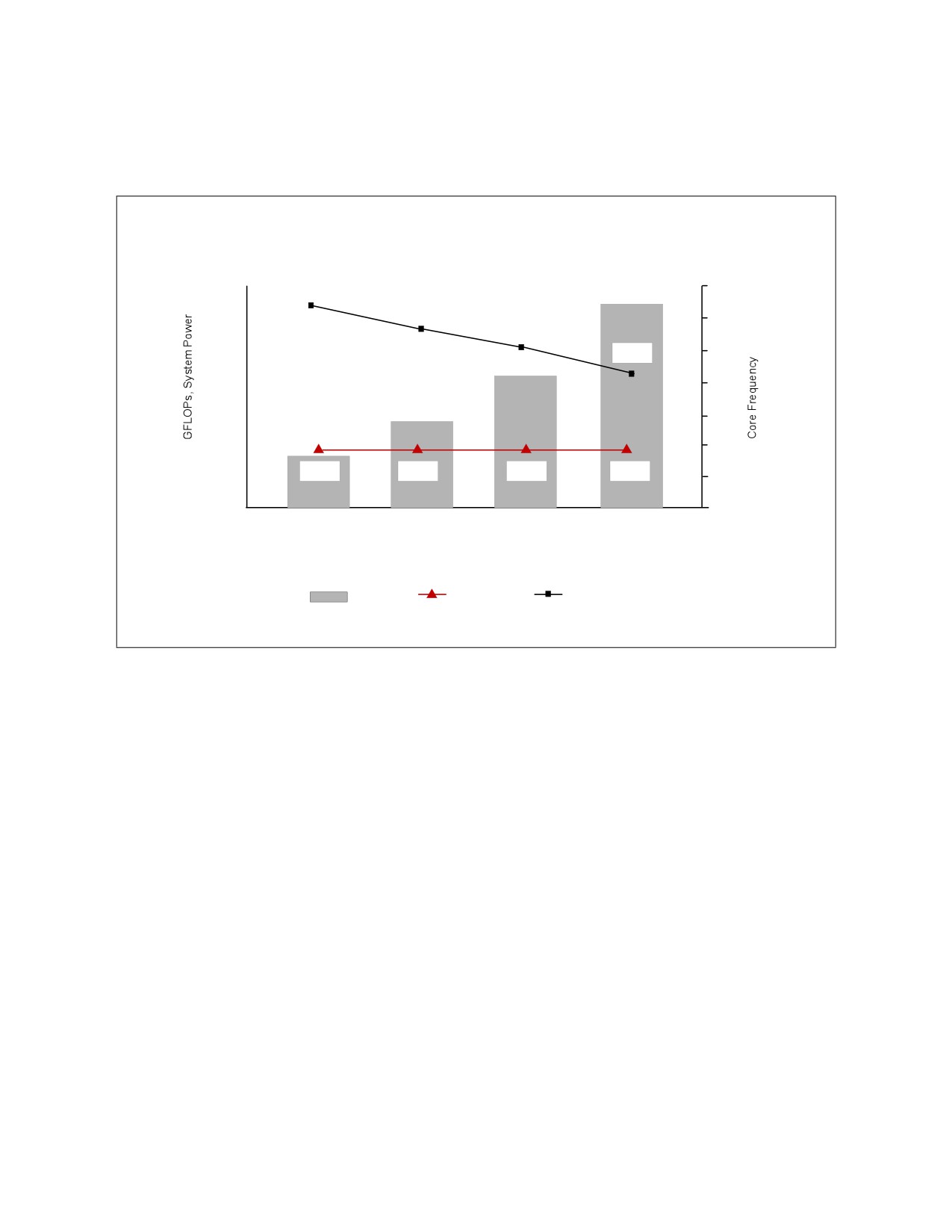
INTEL® 64 AND IA-32 PROCESSOR ARCHITECTURES
Some workloads do not cause the processor to reach its maximum frequency as these workloads are
bound by other factors. For example, the LINPACK benchmark is power limited and does not reach the
processor's maximum frequency. The following graph shows how frequency degrades as vector width
grows, but, despite the frequency drop, performance improves. The data for this graph was collected on
an Intel Xeon Platinum 8180 processor.
LINPACK Performance
3500
3.1
3.5
3259
2.8
3000
3.0
2.5
2500
2.1
2.5
2034
2000
2.0
1500
1178
1.5
760
1000
1.0
500
669
768
791
767
0
SSE4.2
AVX
AVX2
AVX512
GFLOPs
Power (W)
Frequency (GHz)
SOM00061
Figure 2-7. LINPACK Performance
Workloads that execute Intel AVX-512 instructions as a large proportion of their whole instruction count
can gain performance compared to Intel AVX2 instructions, even though they may operate at a lower
frequency. For example, maximum frequency bound Deep Learning workloads that target Intel AVX-512
heavy instructions at a very high percentage can gain 1.3x-1.5x performance improvement vs. the same
workload built to target Intel AVX2 (both operating on Skylake Server microarchitecture).
It is not always easy to predict whether a program's performance will improve from building it to target
Intel AVX-512 instructions. Programs that enjoy high performance gains from the use of xmm or ymm
registers may expect performance improvement by moving to the use of zmm registers. However, some
programs that use zmm registers may not gain as much, or may even lose performance. It is recom-
mended to try multiple build options and measure the performance of the program.
Recommendation: To identify the optimal compiler options to use, build the application with each of the
following set of options and choose the set that provides the best performance.
•
-xCORE-AVX2 -mtune=skylake-avx512 (Linux* and macOS*)
/QxCORE-AVX2 /tune=skylake-avx512 (Windows*)
•
-xCORE-AVX512 -qopt-zmm-usage=low (Linux* and macOS*)
/QxCORE-AVX512 /Qopt-zmm-usage:low (Windows*)
•
-xCORE-AVX512 -qopt-zmm-usage=high (Linux* and macOS*)
/QxCORE-AVX512 /Qopt-zmm-usage:high (Windows*)
See Section 18.26 for more information about these options.
Ref#: 248966-048
2-26
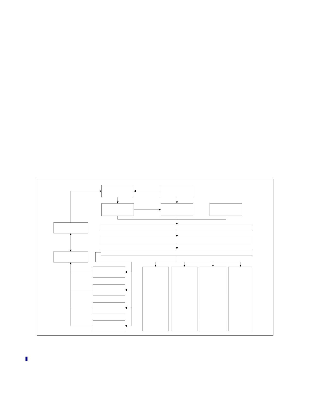
INTEL® 64 AND IA-32 PROCESSOR ARCHITECTURES
The GCC Compiler has the option -mprefer-vector-width=none|128|256|512 to control vector width
preference. While -march=skylake-avx512 is designed to provide the best performance for the Skylake
Server microarchitecture some programs can benefit from different vector width preferences. To identify
the optimal compiler options to use, build the application with each of the following set of options and
choose the set that provides the best performance. -mprefer-vector-width=256 is the default for
skylake-avx512.
•
-march=skylake -mtune=skylake-avx512
•
-march=skylake-avx512
•
-march=skylake-avx512 -mprefer-vector-width=512
Clang/LLVM is currently implementing the option -mprefer-vector-width=none|128|256|512, similar
to GCC. To identify the optimal compiler options to use, build the application with each of the following
set of options and choose the set that provides the best performance.
•
-march=skylake -mtune=skylake-avx512
•
-march=skylake-avx512 (plus -mprefer-vector-width=256, if available)
•
-march=skylake-avx512 (plus -mprefer-vector-width=512, if available)
2.6
SKYLAKE CLIENT MICROARCHITECTURE
The Skylake client microarchitecture builds on the successes of the Haswell and Broadwell microarchitec-
tures. The basic pipeline functionality of the Skylake client microarchitecture is depicted in Figure 2-8.
32K L1
BPU
Instruction Cache
Legacy Decode
Decoded
MSROM
Pipeline
Icache (DSB)
256k L2 Cache
Instruction Decode Queue (IDQ, or Micro-Ops Queue)
(Unified)
Allocate/Rename/Retire/Move Elimination/Zero Idiom
Scheduler
32K L1 Data
Cache
Port 2 LD/STA
Port 0
Port 1
Port 5
Port 6
INTEGER ALU
INTEGER ALU
INTEGER ALU
INTEGER ALU
Fast LEA
Fast LEA
Int Shft
VEC SHUFFLE
Branch 1
Port 3 LD/STA
VEC FMA
VEC FMA
VEC SHUF
VEC MUL
VEC MUL
VEC ALU
Port 4 STD
VEC Add
VEC Add
CVT
VEC ALU
VEC ALU
VEC Shft
VEC Shft
Divide
Int MUL
Port 7 STA
Branch2
Slow LEA
Figure 2-8. CPU Core Pipeline Functionality of the Skylake Client Microarchitecture
Ref#: 248966-048
2-27

INTEL® 64 AND IA-32 PROCESSOR ARCHITECTURES
The Skylake Client microarchitecture offers the following enhancements:
• Larger internal buffers to enable deeper OOO execution and higher cache bandwidth.
• Improved front end throughput.
• Improved branch predictor.
• Improved divider throughput and latency.
• Lower power consumption.
• Improved SMT performance with Hyper-Threading Technology.
• Balanced floating-point ADD, MUL, FMA throughput and latency.
The microarchitecture supports flexible integration of multiple processor cores with a shared uncore
sub-system consisting of a number of components including a ring interconnect to multiple slices of L3
cache (an off-die L4 is optional), processor graphics, integrated memory controller, interconnect fabrics,
etc.
2.6.1
The Front End
The front end in the Skylake Client microarchitecture provides the following improvements over previous
generation microarchitectures:
• Legacy Decode Pipeline delivery of 5 uops per cycle to the IDQ compared to 4 uops in previous gener-
ations.
• The DSB delivers 6 uops per cycle to the IDQ compared to 4 uops in previous generations.
• The IDQ can hold 64 uops per logical processor vs. 28 uops per logical processor in previous
generations when two sibling logical processors in the same core are active (2x64 vs. 2x28 per core).
If only one logical processor is active in the core, the IDQ can hold 64 uops (64 vs. 56 uops in ST
operation).
• The LSD in the IDQ can detect loops up to 64 uops per logical processor irrespective ST or SMT
operation.
• Improved Branch Predictor.
2.6.2
The Out-of-Order Execution Engine
The Out of Order and execution engine changes in Skylake Client microarchitecture include:
• Larger buffers enable deeper OOO execution compared to previous generations.
• Improved throughput and latency for divide/sqrt and approximate reciprocals.
• Identical latency and throughput for all operations running on FMA units.
• Longer pause latency enables better power efficiency and better SMT performance resource utili-
zation.
Ref#: 248966-048
2-28

INTEL® 64 AND IA-32 PROCESSOR ARCHITECTURES
Table 2-11 summarizes the OOO engine’s capability to dispatch different types of operations to various
ports.
Table 2-11. Dispatch Port and Execution Stacks of the Skylake Client Microarchitecture
Port 0
Port 1
Port 2, 3
Port 4
Port 5
Port 6
Port 7
ALU,
ALU,
ALU,
ALU,
LD
Vec ALU
Fast LEA,
STD
Fast LEA,
Shft,
STA
STA
Vec ALU
Vec ALU,
Vec Shft,
Vec Shft,
Vec Shuffle,
Branch1
Vec Add,
Vec Add,
Vec Mul,
Vec Mul,
FMA,
FMA
DIV,
Slow Int
Branch2
Slow LEA
Table 2-12 lists execution units and common representative instructions that rely on these units.
Throughput improvements across the SSE, AVX and general-purpose instruction sets are related to the
number of units for the respective operations, and the varieties of instructions that execute using a
particular unit.
Table 2-12. Skylake Client Microarchitecture Execution Units and Representative Instructions1
Execution
# of
Instructions
Unit
Unit
ALU
4
add, and, cmp, or, test, xor, movzx, movsx, mov, (v)movdqu, (v)movdqa, (v)movap*, (v)movup*
SHFT
2
sal, shl, rol, adc, sarx, adcx, adox, etc.
Slow Int
1
mul, imul, bsr, rcl, shld, mulx, pdep, etc.
BM
2
andn, bextr, blsi, blsmsk, bzhi, etc
(v)pand, (v)por, (v)pxor, (v)movq, (v)movq, (v)movap*, (v)movup*,
Vec ALU
3
(v)andp*, (v)orp*, (v)paddb/w/d/q, (v)blendv*, (v)blendp*, (v)pblendd
Vec_Shft
2
(v)psllv*, (v)psrlv*, vector shift count in imm8
(v)addp*, (v)cmpp*, (v)max*, (v)min*, (v)padds*, (v)paddus*, (v)psign, (v)pabs, (v)pavgb,
Vec Add
2
(v)pcmpeq*, (v)pmax, (v)cvtps2dq, (v)cvtdq2ps, (v)cvtsd2si, (v)cvtss2si
(v)shufp*, vperm*, (v)pack*, (v)unpck*, (v)punpck*, (v)pshuf*, (v)pslldq, (v)alignr, (v)pmovzx*,
Shuffle
1
vbroadcast*, (v)pslldq, (v)psrldq, (v)pblendw
Vec Mul
2
(v)mul*, (v)pmul*, (v)pmadd*,
SIMD Misc
1
STTNI, (v)pclmulqdq, (v)psadw, vector shift count in xmm,
FP Mov
1
(v)movsd/ss, (v)movd gpr,
DIVIDE
1
divp*, divs*, vdiv*, sqrt*, vsqrt*, rcp*, vrcp*, rsqrt*, idiv
NOTES:
1. Execution unit mapping to MMX instructions are not covered in this table. See Section 15.16.5 on MMX instruction
throughput remedy.
Ref#: 248966-048
2-29

INTEL® 64 AND IA-32 PROCESSOR ARCHITECTURES
A significant portion of the Intel SSE, Intel AVX and general-purpose instructions also have latency
improvements. Appendix C lists the specific details. Software-visible latency exposure of an instruction
sometimes may include additional contributions that depend on the relationship between micro-ops flows
of the producer instruction and the micro-op flows of the ensuing consumer instruction. For example, a
two-uop instruction like VPMULLD may experience two cumulative bypass delays of 1 cycle each from
each of the two micro-ops of VPMULLD.
Table 2-13 describes the bypass delay in cycles between a producer uop and the consumer uop. The
left-most column lists a variety of situations characteristic of the producer micro-op. The top row lists a
variety of situations characteristic of the consumer micro-op.
Table 2-13. Bypass Delay Between Producer and Consumer Micro-ops
SIMD/0,1/1
FMA/0,1/4
VIMUL/0,1/4
SIMD/5/1,3
SHUF/5/1,3
V2I/0/3
I2V/5/1
SIMD/0,1/1
0
1
1
0
0
0
NA
FMA/0,1/4
1
0
1
0
0
0
NA
VIMUL/0,1/4
1
0
1
0
0
0
NA
SIMD/5/1,3
0
1
1
0
0
0
NA
SHUF/5/1,3
0
0
1
0
0
0
NA
V2I/0/3
NA
NA
NA
NA
NA
NA
NA
I2V/5/1
0
0
1
0
0
0
NA
The attributes that are relevant to the producer/consumer micro-ops for bypass are a triplet of abbrevi-
ation/one or more port number/latency cycle of the uop. For example:
•
“SIMD/0,1/1” applies to 1-cycle vector SIMD uop dispatched to either port 0 or port 1.
•
“VIMUL/0,1/4” applies to 4-cycle vector integer multiply uop dispatched to either port 0 or port 1.
•
“SIMD/5/1,3” applies to either 1-cycle or 3-cycle non-shuffle uop dispatched to port 5.
2.6.3
Cache and Memory Subsystem
The cache hierarchy of the Skylake Client microarchitecture has the following enhancements:
• Higher Cache bandwidth compared to previous generations.
• Simultaneous handling of more loads and stores enabled by enlarged buffers.
• Processor can do two page walks in parallel compared to one in Haswell microarchitecture and earlier
generations.
• Page split load penalty down from 100 cycles in previous generation to 5 cycles.
• L3 write bandwidth increased from 4 cycles per line in previous generation to 2 per line.
• Support for the CLFLUSHOPT instruction to flush cache lines and manage memory ordering of flushed
data using SFENCE.
• Reduced performance penalty for a software prefetch that specifies a NULL pointer.
• L2 associativity changed from 8 ways to 4 ways.
Ref#: 248966-048
2-30

INTEL® 64 AND IA-32 PROCESSOR ARCHITECTURES
Table 2-14. Cache Parameters of the Skylake Client Microarchitecture
Capacity /
Line Size
Fastest
Peak Bandwidth
Sustained Bandwidth
Update
Level
Associativity
(bytes)
Latency1
(bytes/cyc)
(bytes/cyc)
Policy
96 (2x32B Load +
First Level Data
32 KB/ 8
64
4 cycle
~81
Writeback
1*32B Store)
Instruction
32 KB/8
64
N/A
N/A
N/A
N/A
Second Level
256KB/4
64
12 cycle
64
~29
Writeback
Up to 2MB
Third Level
44
per core/Up
64
32
~18
Writeback
(Shared L3)
to 16 ways
NOTES:
1. Software-visible latency will vary depending on access patterns and other factors.
The TLB hierarchy consists of dedicated level one TLB for instruction cache, TLB for L1D, plus unified TLB
for L2. The partition column of Table 2-15 indicates the resource sharing policy when Hyper-Threading
Technology is active.
Table 2-15. TLB Parameters of the Skylake Client Microarchitecture
Level
Page Size
Entries
Associativity
Partition
Instruction
4KB
128
8 ways
dynamic
Instruction
2MB/4MB
8 per thread
fixed
First Level Data
4KB
64
4
fixed
First Level Data
2MB/4MB
32
4
fixed
First Level Data
1GB
4
4
fixed
Second Level
Shared by 4KB and 2/4MB pages
1536
12
fixed
Second Level
1GB
16
4
fixed
2.6.4
Pause Latency in Skylake Client Microarchitecture
The PAUSE instruction is typically used with software threads executing on two logical processors located
in the same processor core, waiting for a lock to be released. Such short wait loops tend to last between
tens and a few hundreds of cycles, so performance-wise it is better to wait while occupying the CPU than
yielding to the OS. When the wait loop is expected to last for thousands of cycles or more, it is preferable
to yield to the operating system by calling an OS synchronization API function, such as WaitForSingleO-
bject on Windows* OS or futex on Linux.
The PAUSE instruction is intended to:
• Temporarily provide the sibling logical processor (ready to make forward progress exiting the spin
loop) with competitively shared hardware resources. The competitively-shared microarchitectural
resources that the sibling logical processor can utilize in the Skylake Client microarchitecture are
listed below.
— Front end slots in the Decode ICache, LSD and IDQ.
— Execution slots in the RS.
• Save power consumed by the processor core compared with executing equivalent spin loop
instruction sequence in the following configurations.
— One logical processor is inactive (e.g., entering a C-state).
— Both logical processors in the same core execute the PAUSE instruction.
Ref#: 248966-048
2-31

INTEL® 64 AND IA-32 PROCESSOR ARCHITECTURES
— HT is disabled (e.g. using BIOS options).
The latency of the PAUSE instruction in prior generation microarchitectures is about 10 cycles, whereas
in Skylake Client microarchitecture it has been extended to as many as 140 cycles.
The increased latency (allowing more effective utilization of competitively-shared microarchitectural
resources to the logical processor ready to make forward progress) has a small positive performance
impact of 1-2% on highly threaded applications. It is expected to have negligible impact on less threaded
applications if forward progress is not blocked executing a fixed number of looped PAUSE instructions.
There's also a small power benefit in 2-core and 4-core systems.
As the PAUSE latency has been increased significantly, workloads that are sensitive to PAUSE latency will
suffer some performance loss.
The following is an example of how to use the PAUSE instruction with a dynamic loop iteration count.
Notice that in the Skylake Client microarchitecture the RDTSC instruction counts at the machine's guar-
anteed P1 frequency independently of the current processor clock (see the INVARIANT TSC property),
and therefore, when running in Intel® Turbo-Boost-enabled mode, the delay will remain constant, but
the number of instructions that could have been executed will change.
Use Poll Delay function in your lock to wait a given amount of guaranteed P1 frequency cycles, specified
in the “clocks” variable.
Example 2-8. Dynamic Pause Loop Example
#include <x86intrin.h>
#include <stdint.h>
/* A useful predicate for dealing with timestamps that may wrap.
Is a before b? Since the timestamps may wrap, this is asking whether it's
shorter to go clockwise from a to b around the clock-face, or anti-clockwise.
Times where going clockwise is less distance than going anti-clockwise
are in the future, others are in the past. e.g. a = MAX-1, b = MAX+1 (=0),
then a > b (true) does not mean a reached b; whereas signed(a) = -2,
signed(b) = 0 captures the actual difference */
static inline bool before(uint64_t a, uint64_t b)
{
return ((int64_t)b - (int64_t)a) > 0;
}
void pollDelay(uint32_t clocks)
{
uint64_t endTime = _rdtsc()+ clocks;
for (; before(_rdtsc(), endTime); )
_mm_pause();
}
For contended spinlocks of the form shown in the baseline example below, we recommend an exponen-
tial back off when the lock is found to be busy, as shown in the improved example, to avoid significant
performance degradation that can be caused by conflicts between threads in the machine. This is more
important as we increase the number of threads in the machine and make changes to the architecture
that might aggravate these conflict conditions. In multi-socket Intel server processors with shared
memory, conflicts across threads take much longer to resolve as the number of threads contending for
the same lock increases. The exponential back off is designed to avoid these conflicts between the
threads thus avoiding the potential performance degradation. Note that in the example below, the
Ref#: 248966-048
2-32

INTEL® 64 AND IA-32 PROCESSOR ARCHITECTURES
number of PAUSE instructions are increased by a factor of 2 until some MAX_BACKOFF is reached which
is subject to tuning.
Example 2-9. Contended Locks with Increasing Back-off Example
/*******************/
/*Baseline Version */
/*******************/
// atomic {if (lock == free) then change lock state to busy}
while (cmpxchg(lock, free, busy) == fail)
{
while (lock == busy)
{
__asm__ ("pause");
}
}
/*******************/
/*Improved Version */
/*******************/
int mask = 1;
int const max = 64; //MAX_BACKOFF
while (cmpxchg(lock, free, busy) == fail)
{
while (lock == busy)
{
for (int i=mask; i; --i){
__asm__ ("pause");
}
mask = mask < max ? mask<<1 : max;
}
}
2.7
INTEL® HYPER-THREADING TECHNOLOGY (INTEL® HT TECHNOLOGY)
Intel® Hyper-Threading Technology (Intel® HT Technology) enables software to take advantage of
task-level, or thread-level parallelism by providing multiple logical processors within a physical processor
package, or within each processor core in a physical processor package. In its first implementation in the
Intel® Xeon® processor, Intel HT Technology makes a single physical processor (or a processor core)
appear as two or more logical processors.
Most Intel Architecture processor families support Intel HT Technology with two logical processors in each
processor core, or in a physical processor in early implementations. The rest of this section describes
features of the early implementation of Intel HT Technology. Most of the descriptions also apply to later
implementations supporting two logical processors. The microarchitecture sections in this chapter
provide additional details to individual microarchitecture and enhancements to Intel HT Technology.
The two logical processors each have a complete set of architectural registers while sharing one single
physical processor's resources. By maintaining the architecture state of two processors, an Intel HT
Technology-capable processor looks like two processors to software, including operating system and
application code.
Ref#: 248966-048
2-33

INTEL® 64 AND IA-32 PROCESSOR ARCHITECTURES
By sharing resources needed for peak demands between two logical processors, Intel HT Technology is
well suited for multiprocessor systems to provide an additional performance boost in throughput when
compared to traditional MP systems.
Figure 2-9 shows a typical bus-based symmetric multiprocessor (SMP) based on processors supporting
Intel HT Technology. Each logical processor can execute a software thread, allowing a maximum of two
software threads to execute simultaneously on one physical processor. The two software threads execute
simultaneously, meaning that in the same clock cycle an “add” operation from logical processor 0 and
another “add” operation and load from logical processor 1 can be executed simultaneously by the execu-
tion engine.
In the first implementation of Intel HT Technology, the physical execution resources are shared and the
architecture state is duplicated for each logical processor. This minimizes the die area cost of imple-
menting Intel HT Technology while still achieving performance gains for multithreaded applications or
multitasking workloads.
Architectural
Architectural
Architectural
Architectural
State
State
State
State
Execution Engine
Execution Engine
Local
APIC
Local APIC
Local
APIC
Local APIC
Bus Interface
Bus Interface
System Bus
Figure 2-9. Intel® Hyper-Threading Technology on an SMP System
The performance potential due to Intel HT Technology is due to:
• The fact that operating systems and user programs can schedule processes or threads to execute
simultaneously on the logical processors in each physical processor.
• The ability to use on-chip execution resources at a higher level than when only a single thread is
consuming the execution resources; higher level of resource utilization can lead to higher system
throughput.
2.7.1
Processor Resources and Intel® HT Technology
The majority of microarchitecture resources in a physical processor are shared between the logical
processors. Only a few small data structures were replicated for each logical processor. This section
describes how resources are shared, partitioned or replicated.
2.7.1.1
Replicated Resources
The architectural state is replicated for each logical processor. The architecture state consists of registers
that are used by the operating system and application code to control program behavior and store data
for computations. This state includes the eight general-purpose registers, the control registers, machine
state registers, debug registers, and others. There are a few exceptions, most notably the memory type
Ref#: 248966-048
2-34
INTEL® 64 AND IA-32 PROCESSOR ARCHITECTURES
range registers (MTRRs) and the performance monitoring resources. For a complete list of the architec-
ture state and exceptions, see the Intel® 64 and IA-32 Architectures Software Developer’s Manual,
Volumes 3A, 3B, 3C, & 3D.
Other resources such as instruction pointers and register renaming tables were replicated to simultane-
ously track execution and state changes of the two logical processors. The return stack predictor is repli-
cated to improve branch prediction of return instructions.
In addition, a few buffers (for example, the two-entry instruction streaming buffers) were replicated to
reduce complexity.
2.7.1.2
Partitioned Resources
Several buffers are shared by limiting the use of each logical processor to half the entries. These are
referred to as partitioned resources. Reasons for this partitioning include:
• Operational fairness.
• Permitting the ability to allow operations from one logical processor to bypass operations of the other
logical processor that may have stalled.
For example: a cache miss, a branch misprediction, or instruction dependencies may prevent a logical
processor from making forward progress for some number of cycles. The partitioning prevents the stalled
logical processor from blocking forward progress.
In general, the buffers for staging instructions between major pipe stages are partitioned. These buffers
include µop queues after the execution trace cache, the queues after the register rename stage, the
reorder buffer which stages instructions for retirement, and the load and store buffers.
In the case of load and store buffers, partitioning also provided an easier implementation to maintain
memory ordering for each logical processor and detect memory ordering violations.
2.7.1.3
Shared Resources
Most resources in a physical processor are fully shared to improve the dynamic utilization of the resource,
including caches and all the execution units. Some shared resources which are linearly addressed, like
the DTLB, include a logical processor ID bit to distinguish whether the entry belongs to one logical
processor or the other.
2.7.2
Microarchitecture Pipeline and Intel® HT Technology
This section describes the Intel HT Technology microarchitecture and how instructions from the two
logical processors are handled between the front end and the back end of the pipeline.
Although instructions originating from two programs or two threads execute simultaneously and not
necessarily in program order in the execution core and memory hierarchy, the front end and back end
contain several selection points to select between instructions from the two logical processors. All selec-
tion points alternate between the two logical processors unless one logical processor cannot make use of
a pipeline stage. In this case, the other logical processor has full use of every cycle of the pipeline stage.
Reasons why a logical processor may not use a pipeline stage include cache misses, branch mispredic-
tions, and instruction dependencies.
2.7.3
Execution Core
The core can dispatch up to six µops per cycle, provided the µops are ready to execute. Once the µops
are placed in the queues waiting for execution, there is no distinction between instructions from the two
logical processors. The execution core and memory hierarchy is also oblivious to which instructions
belong to which logical processor.
Ref#: 248966-048
2-35
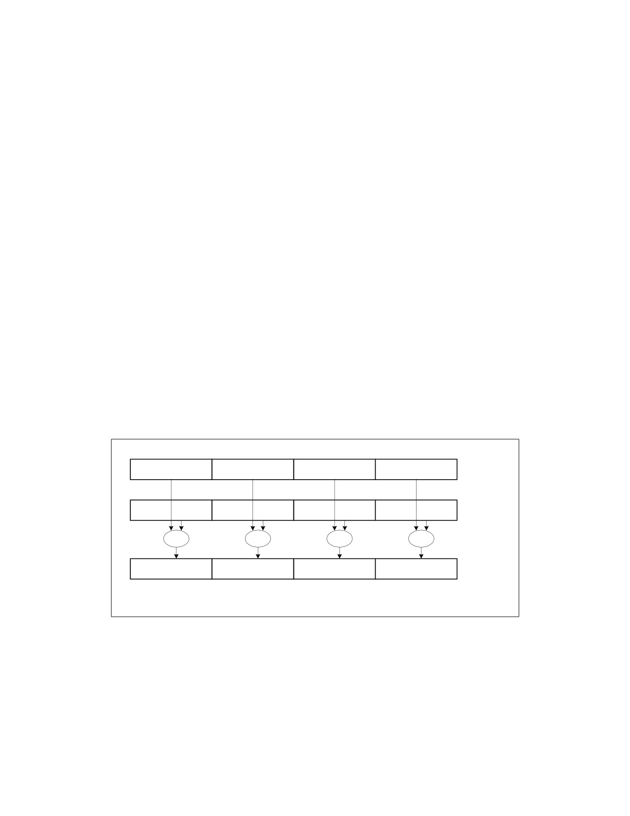
INTEL® 64 AND IA-32 PROCESSOR ARCHITECTURES
After execution, instructions are placed in the re-order buffer. The re-order buffer decouples the execu-
tion stage from the retirement stage. The re-order buffer is partitioned such that each uses half the
entries.
2.7.4
Retirement
The retirement logic tracks when instructions from the two logical processors are ready to be retired. It
retires the instruction in program order for each logical processor by alternating between the two logical
processors. If one logical processor is not ready to retire any instructions, then all retirement bandwidth
is dedicated to the other logical processor.
Once stores have retired, the processor needs to write the store data into the level-one data cache.
Selection logic alternates between the two logical processors to commit store data to the cache.
2.8
SIMD TECHNOLOGY
SIMD computations (see Figure 2-10) were introduced to the architecture with MMX technology. MMX
technology allows SIMD computations to be performed on packed byte, word, and doubleword integers.
The integers are contained in a set of eight 64-bit registers called MMX registers (see Figure 2-11).
The Pentium III processor extended the SIMD computation model with the introduction of the Streaming
SIMD Extensions (SSE). SSE allows SIMD computations to be performed on operands that contain four
packed single-precision floating-point data elements. The operands can be in memory or in a set of eight
128-bit XMM registers (see Figure 2-11). SSE also extended SIMD computational capability by adding
additional 64-bit MMX instructions.
Figure 2-10 shows a typical SIMD computation. Two sets of four packed data elements (X1, X2, X3, and
X4, and Y1, Y2, Y3, and Y4) are operated on in parallel, with the same operation being performed on each
corresponding pair of data elements (X1 and Y1, X2 and Y2, X3 and Y3, and X4 and Y4). The results of
the four parallel computations are sorted as a set of four packed data elements.
X4
X3
X2
X1
Y4
Y3
Y2
Y1
OP
OP
OP
OP
X4 op Y4
X3 op Y3
X2 op Y2
X1 op Y1
OM15148
Figure 2-10. Typical SIMD Operations
The Pentium 4 processor further extended the SIMD computation model with the introduction of
Streaming SIMD Extensions 2 (SSE2), Streaming SIMD Extensions 3 (SSE3), and Intel Xeon processor
5100 series introduced Supplemental Streaming SIMD Extensions 3 (SSSE3).
SSE2 works with operands in either memory or in the XMM registers. The technology extends SIMD
computations to process packed double-precision floating-point data elements and 128-bit packed inte-
Ref#: 248966-048
2-36

INTEL® 64 AND IA-32 PROCESSOR ARCHITECTURES
gers. There are 144 instructions in SSE2 that operate on two packed double-precision floating-point data
elements or on 16 packed byte, 8 packed word, 4 doubleword, and 2 quadword integers.
SSE3 enhances x87, SSE and SSE2 by providing 13 instructions that can accelerate application perfor-
mance in specific areas. These include video processing, complex arithmetics, and thread synchroniza-
tion. SSE3 complements SSE and SSE2 with instructions that process SIMD data asymmetrically,
facilitate horizontal computation, and help avoid loading cache line splits. See Figure 2-11.
SSSE3 provides additional enhancement for SIMD computation with 32 instructions on digital video and
signal processing.
SSE4.1, SSE4.2 and AESNI are additional SIMD extensions that provide acceleration for applications in
media processing, text/lexical processing, and block encryption/decryption.
The SIMD extensions operates the same way in Intel 64 architecture as in IA-32 architecture, with the
following enhancements:
•
128-bit SIMD instructions referencing XMM register can access 16 XMM registers in 64-bit mode.
• Instructions that reference 32-bit general purpose registers can access 16 general purpose registers
in 64-bit mode.
64-bit MMX Registers
128-bit XMM Registers
MM7
XMM7
MM6
XMM6
MM5
XMM5
MM4
XMM4
MM3
XMM3
MM2
XMM2
MM1
XMM1
MM0
XMM0
OM15149
Figure 2-11. SIMD Instruction Register Usage
SIMD improves the performance of 3D graphics, speech recognition, image processing, scientific applica-
tions and applications that have the following characteristics:
• Inherently parallel.
• Recurring memory access patterns.
• Localized recurring operations performed on the data.
• Data-independent control flow.
2.9
SUMMARY OF SIMD TECHNOLOGIES AND APPLICATION LEVEL
EXTENSIONS
SIMD floating-point instructions fully support the IEEE Standard 754 for Binary Floating-Point Arithmetic.
They are accessible from all IA-32 execution modes: protected mode, real address mode, and Virtual
8086 mode.
Ref#: 248966-048
2-37
INTEL® 64 AND IA-32 PROCESSOR ARCHITECTURES
SSE, SSE2, and MMX technologies are architectural extensions. Existing software will continue to run
correctly, without modification on Intel microprocessors that incorporate these technologies. Existing
software will also run correctly in the presence of applications that incorporate SIMD technologies.
SSE and SSE2 instructions also introduced cacheability and memory ordering instructions that can
improve cache usage and application performance.
For more on SSE, SSE2, SSE3 and MMX technologies, see the following chapters in the Intel® 64 and
IA-32 Architectures Software Developer’s Manual, Volume 1
• Chapter 9, “Programming with Intel® MMX™ Technology.”
• Chapter 10, “Programming with Intel® Streaming SIMD Extensions (Intel® SSE).”
• Chapter 11, “Programming with Intel® Streaming SIMD Extensions 2 (Intel® SSE2).”
• Chapter 12, “Programming with Intel® SSE3, SSSE3, Intel® SSE4, and Intel® AES-NI.”
• Chapter 14, “Programming with Intel® AVX, FMA, and Intel® AVX2.”
• Chapter 15, “Programming with Intel® AVX-512.”
• Chapter 16, “Programming with Intel® Transactional Synchronization Extensions.”
2.9.1
MMX™ Technology
MMX Technology introduced:
•
64-bit MMX registers.
• Support for SIMD operations on packed byte, word, and doubleword integers.
Recommendation: Integer SIMD code written using MMX instructions should consider more efficient
implementations using SSE/Intel AVX instructions.
2.9.2
Streaming SIMD Extensions
Streaming SIMD extensions introduced:
•
128-bit XMM registers.
•
128-bit data type with four packed single-precision floating-point operands.
• Data prefetch instructions.
• Non-temporal store instructions and other cacheability and memory ordering instructions.
• Extra 64-bit SIMD integer support.
SSE instructions are useful for 3D geometry, 3D rendering, speech recognition, and video encoding and
decoding.
2.9.3
Streaming SIMD Extensions 2
Streaming SIMD extensions 2 add the following:
•
128-bit data type with two packed double-precision floating-point operands.
•
128-bit data types for SIMD integer operation on 16-byte, 8-word, 4-doubleword, or 2-quadword
integers.
• Support for SIMD arithmetic on 64-bit integer operands.
• Instructions for converting between new and existing data types.
• Extended support for data shuffling.
• Extended support for cacheability and memory ordering operations.
SSE2 instructions are useful for 3D graphics, video decoding/encoding, and encryption.
Ref#: 248966-048
2-38
INTEL® 64 AND IA-32 PROCESSOR ARCHITECTURES
2.9.4
Streaming SIMD Extensions 3
Streaming SIMD extensions 3 add the following:
• SIMD floating-point instructions for asymmetric and horizontal computation.
• A special-purpose 128-bit load instruction to avoid cache line splits.
• An x87 FPU instruction to convert to integer independent of the floating-point control word (FCW).
• Instructions to support thread synchronization.
SSE3 instructions are useful for scientific, video and multi-threaded applications.
2.9.5
Supplemental Streaming SIMD Extensions 3
The Supplemental Streaming SIMD Extensions 3 introduces 32 new instructions to accelerate eight
types of computations on packed integers. These include:
•
12 instructions that perform horizontal addition or subtraction operations.
•
6 instructions that evaluate the absolute values.
•
2 instructions that perform multiply and add operations and speed up the evaluation of dot products.
•
2 instructions that accelerate packed-integer multiply operations and produce integer values with
scaling.
•
2 instructions that perform a byte-wise, in-place shuffle according to the second shuffle control
operand.
•
6 instructions that negate packed integers in the destination operand if the signs of the corre-
sponding element in the source operand is less than zero.
•
2 instructions that align data from the composite of two operands.
2.9.6
SSE4.1
SSE4.1 introduces 47 new instructions to accelerate video, imaging and 3D applications. SSE4.1 also
improves compiler vectorization and significantly increase support for packed dword computation. These
include:
• Two instructions perform packed dword multiplies.
• Two instructions perform floating-point dot products with input/output selects.
• One instruction provides a streaming hint for WC loads.
• Six instructions simplify packed blending.
• Eight instructions expand support for packed integer MIN/MAX.
• Four instructions support floating-point round with selectable rounding mode and precision exception
override.
• Seven instructions improve data insertion and extractions from XMM registers
• Twelve instructions improve packed integer format conversions (sign and zero extensions).
• One instruction improves SAD (sum absolute difference) generation for small block sizes.
• One instruction aids horizontal searching operations of word integers.
• One instruction improves masked comparisons.
• One instruction adds qword packed equality comparisons.
• One instruction adds dword packing with unsigned saturation.
2.9.7
SSE4.2
SSE4.2 introduces 7 new instructions. These include:
Ref#: 248966-048
2-39
INTEL® 64 AND IA-32 PROCESSOR ARCHITECTURES
• A 128-bit SIMD integer instruction for comparing 64-bit integer data elements.
• Four string/text processing instructions providing a rich set of primitives, these primitives can
accelerate:
— Basic and advanced string library functions from strlen, strcmp, to strcspn.
— Delimiter processing, token extraction for lexing of text streams.
— Parser, schema validation including XML processing.
• A general-purpose instruction for accelerating cyclic redundancy checksum signature calculations.
• A general-purpose instruction for calculating bit count population of integer numbers.
2.9.8
AESNI and PCLMULQDQ
AESNI introduces seven new instructions, six of them are primitives for accelerating algorithms based on
AES encryption/decryption standard, referred to as AESNI.
The PCLMULQDQ instruction accelerates general-purpose block encryption, which can perform carry-less
multiplication for two binary numbers up to 64-bit wide.
Typically, algorithm based on AES standard involve transformation of block data over multiple iterations
via several primitives. The AES teration.
AES encryption involves processing 128-bit input data (plain text) through a finite number of iterative
operation, referred to as “AES round”, into a 128-bit encrypted block (ciphertext). Decryption follows the
reverse direction of iterative operation using the “equivalent inverse cipher” instead of the “inverse
cipher”.
The cryptographic processing at each round involves two input data, one is the “state”, the other is the
“round key”. Each round uses a different “round key”. The round keys are derived from the cipher key
using a “key schedule” algorithm. The “key schedule” algorithm is independent of the data processing of
encryption/decryption, and can be carried out independently from the encryption/decryption phase.
The AES extensions provide two primitives to accelerate AES rounds on encryption, two primitives for
AES rounds on decryption using the equivalent inverse cipher, and two instructions to support the AES
key expansion procedure.
2.9.9
Intel® Advanced Vector Extensions (Intel® AVX)
Intel® Advanced Vector Extensions (Intel® AVX) offers comprehensive architectural enhancements over
previous generations of Streaming SIMD Extensions. Intel AVX introduces the following architectural
enhancements:
• Support for 256-bit wide vectors and SIMD register set.
•
256-bit floating-point instruction set enhancement with up to 2X performance gain relative to 128-bit
Streaming SIMD extensions.
• Instruction syntax support for generalized three-operand syntax to improve instruction programming
flexibility and efficient encoding of new instruction extensions.
• Enhancement of legacy 128-bit SIMD instruction extensions to support three-operand syntax and to
simplify compiler vectorization of high-level language expressions.
• Support flexible deployment of 256-bit AVX code, 128-bit AVX code, legacy 128-bit code and scalar
code.
Intel AVX instruction set and 256-bit register state management detail are described in Intel® 64 and
IA-32 Architectures Software Developer’s Manual, Volumes 2A, 2B, 2C, & 2D. Optimization techniques
for Intel AVX are discussed in Chapter 15, “Optimizations for Intel® AVX, Intel® AVX2, and Intel® FMA.”
Ref#: 248966-048
2-40
INTEL® 64 AND IA-32 PROCESSOR ARCHITECTURES
2.9.10 Half-Precision Floating-Point Conversion (F16C)
VCVTPH2PS and VCVTPS2PH are two instructions supporting half-precision floating-point data type
conversion to and from single-precision floating-point data types. These two instruction extends on the
same programming model as Intel AVX.
2.9.11 RDRAND
The RDRAND instruction retrieves a random number supplied by a cryptographically secure, determin-
istic random bit generator (DBRG). The DBRG is designed to meet NIST SP 800-90A standard.
2.9.12 Fused-Multiply-ADD (FMA) Extensions
FMA extensions enhances Intel AVX with high-throughput, arithmetic capabilities covering fused
multiply-add, fused multiply-subtract, fused multiply add/subtract interleave, signed-reversed multiply
on fused multiply-add and multiply-subtract operations. FMA extensions provide 36 256-bit
floating-point instructions to perform computation on 256-bit vectors and additional 128-bit and scalar
FMA instructions.
2.9.13 Intel® Advanced Vector Extensions 2 (Intel® AVX2)
Intel® AVX2 extends Intel AVX by promoting most of the 128-bit SIMD integer instructions with 256-bit
numeric processing capabilities. Intel AVX2 instructions follow the same programming model as AVX
instructions.
In addition, Intel AVX2 provide enhanced functionalities for broadcast/permute operations on data
elements, vector shift instructions with variable-shift count per data element, and instructions to fetch
non-contiguous data elements from memory.
2.9.14 General-Purpose Bit-Processing Instructions
The fourth generation Intel Core processor family introduces a collection of bit processing instructions
that operate on the general purpose registers. The majority of these instructions uses the VEX-prefix
encoding scheme to provide non-destructive source operand syntax.
There instructions are enumerated by three separate feature flags reported by CPUID. For details, see
Section 5.1 of Intel® 64 and IA-32 Architectures Software Developer’s Manual, Volume 1 and chapters
3, 4 and 5 of the Intel® 64 and IA-32 Architectures Software Developer’s Manual, Volumes 2A, 2B, 2C,
& 2D.
2.9.15 Intel® Transactional Synchronization Extensions (Intel® TSX)
The fourth generation Intel Core processor family introduces Intel® Transactional Synchronization Exten-
sions (Intel® TSX), which aim to improve the performance of lock-protected critical sections of multi-
threaded applications while maintaining the lock-based programming model.
For backg11round and details, see Chapter 16 of Intel® 64 and IA-32 Architectures Software Developer’s
Manual, Volume 1.
Software tuning recommendations for using Intel TSX on lock-protected critical sections of multithreaded
applications are described in Chapter 16, “Intel® TSX Recommendations.”
Ref#: 248966-048
2-41
INTEL® 64 AND IA-32 PROCESSOR ARCHITECTURES
2.9.16 RDSEED
The RDSEED instruction retrieves a random number supplied by a cryptographically secure, enhanced
deterministic random bit generator Enhanced NRBG). The NRBG is designed to meet the NIST SP
800-90B and NIST SP 800-90C standards.
2.9.17 ADCX and ADOX Instructions
The ADCX and ADOX instructions, in conjunction with MULX instruction, enable software to speed up
calculations that require large integer numerics.
Ref#: 248966-048
2-42
2. Updates to Chapter 3
Change bars and violet text show changes to Chapter 3 of the Intel® 64 and IA-32 Architectures Optimization
Reference Manual: Intel® 64 and IA-32 Processor Architectures.
------------------------------------------------------------------------------------------
Changes to this chapter:
• Corrected branding and style across chapter.
• Section 3.4
— Removed section referring to the updates in Intel® Core Duo.
• Section 3.5
— Updated Figure 3-1 to match style of those in Chapter 2
• Section 3.6:
— 3.6.1: added- Bank conflicts may occur with the introduction due to the third load port in the Golden Cove
microarchitecture. In this microarchitecture, conflicts happen between three loads with the same bits 2-5
of their linear address even if they access the same set of the cache. Up to two loads can access the same
cache bank without a conflict; however, a third load accessing the same bank must be delayed. The bank
conflicts do not apply to 512-bit wide loads because their bandwidth is limited to two per cycle.
Recommendation: In the Golden Cove microarchitecture, bank conflicts often happen when multiple
loads access the same memory location. Whenever possible, avoid reading the same memory location
within a tight loop or using multiple load operations. Commonly used memory locations are better kept in
the registers to prevent potential bank conflict penalty.
• Section 3.11:
— Added Section: 3.11.5: False Sharing.
Intel® 64 and IA-32 Architectures Optimization Reference Manual
13

GENERAL OPTIMIZATION GUIDELINES
CHAPTER 3
GENERAL OPTIMIZATION GUIDELINES
This chapter discusses general optimization techniques that can improve the performance of applications
running on Intel® processors. These techniques take advantage of microarchitectural features described
in Chapter 2, “Intel® 64 and IA-32 Processor Architectures.” Optimization guidelines focusing on Intel
multi-core processors, Hyper-Threading Technology, and 64-bit mode applications are discussed in
Chapter 11, “Multicore and Intel® Hyper-Threading Technology (Intel® HT),” and Chapter 13, “64-bit
Mode Coding Guidelines.”
Practices that optimize performance focus on three areas:
• Tools and techniques for code generation.
• Analysis of the performance characteristics of the workload and its interaction with microarchitectural
sub-systems.
• Tuning code to the target microarchitecture (or families of microarchitecture) to improve perfor-
mance.
Some hints on using tools are summarized first to simplify the first two tasks. The rest of the chapter will
focus on recommendations for code generation or code tuning to the target microarchitectures.
This chapter explains optimization techniques for the Intel® C++ Compiler, the Intel® Fortran Compiler,
and other compilers.
3.1
PERFORMANCE TOOLS
Intel offers several tools to help optimize application performance, including compilers, performance
analysis, and multithreading tools.
3.1.1
Intel® C++ and Fortran Compilers
Intel compilers support multiple operating systems (Windows*, Linux*, Mac OS*, and embedded). The
Intel compilers optimize performance and give application developers access to advanced features,
including:
• Flexibility to target 32-bit or 64-bit Intel processors for optimization.
• Compatibility with many integrated development environments or third-party compilers.
• Automatic optimization features to take advantage of the target processor’s architecture.
• Automatic compiler optimization reduces the need to write different code for different processors.
• Common compiler features that are supported across Windows, Linux, and Mac OS include:
— General optimization settings.
— Cache-management features.
— Interprocedural optimization (IPO) methods.
— Profile-guided optimization (PGO) methods.
— Multithreading support.
— Floating-point arithmetic precision and consistency support.
— Compiler optimization and vectorization reports.
Ref#: 248966-048
3-1
GENERAL OPTIMIZATION GUIDELINES
3.1.2
General Compiler Recommendations
Generally speaking, a compiler tuned for a target microarchitecture can be expected to match or outper-
form hand-coding. However, if performance problems are noted with the compiled code, some compilers
(like Intel C++ and Fortran compilers) allow the coder to insert intrinsics or inline assembly to exert
control over generated code. If inline assembly is used, the user must verify that the code generated is
high quality and yields good performance.
Default compiler switches are targeted for common cases. An optimization may be made to the compiler
default if it benefits most programs. If the root cause of a performance problem is a poor choice on the
part of the compiler, using different switches or compiling the targeted module with a different compiler
may be the solution. See the “Quick Reference Guide to Optimization with Intel® C++ and Fortran
Compilers” for additional suggestions on compiler Optimization Options, including processor-specific
ones.
3.1.3
VTune™ Performance Analyzer
VTune uses performance monitoring hardware to collect statistics and coding information about your
application and its interaction with the microarchitecture. This allows software engineers to measure
performance characteristics of the workload for a given microarchitecture. VTune supports all current
and past Intel processor families.
The VTune Performance Analyzer provides two kinds of feedback:
• Indication of a performance improvement gained by using a specific coding recommendation or
microarchitectural feature.
• Information on whether a change in the program has improved or degraded performance with
respect to a particular metric.
The VTune Performance Analyzer also provides measures for a number of workload characteristics,
including:
• Retirement throughput of instruction execution as an indication of the degree of extractable
instruction-level parallelism in the workload.
• Data traffic locality as an indication of the stress point of the cache and memory hierarchy.
• Data traffic parallelism as an indication of the degree of effectiveness of amortization of data access
latency.
NOTE
Improving performance in one part of the machine does not necessarily bring significant
gains to overall performance. It is possible to degrade overall performance by improving
performance for some particular metric.
Where appropriate, coding recommendations in this chapter include descriptions of the VTune Perfor-
mance Analyzer events that provide measurable data on the performance gain achieved by following the
recommendations. For more on using the VTune analyzer, refer to the application’s online help.
3.2
PROCESSOR PERSPECTIVES
Many coding recommendations work well across current microarchitectures. However, there are situa-
tions where a recommendation may benefit one microarchitecture more than another.
3.2.1
CPUID Dispatch Strategy and Compatible Code Strategy
When optimum performance on all processor generations is desired, applications can take advantage of
the CPUID instruction to identify the processor generation and integrate processor-specific instructions
Ref#: 248966-048
3-2
GENERAL OPTIMIZATION GUIDELINES
into the source code. The Intel C++ Compiler supports the integration of different versions of the code
for different target processors. The selection of which code to execute at runtime is made based on the
CPU identifiers. Binary code targeted for different processor generations can be generated under the
control of the programmer or by the compiler. Refer to the “Intel® C++ Compiler Classic Developer
Guide and Reference” cpu_dispatch and cpu_specific sections for more information on CPU dispatching
(a.k.a function multi-versioning).
For applications that target multiple generations of microarchitectures, and where minimum binary code
size and single code path is important, a compatible code strategy is the best. Optimizing applications
using techniques developed for the Intel Core microarchitecture combined with Nehalem microarchitec-
ture are likely to improve code efficiency and scalability when running on processors based on current
and future generations of Intel 64 and IA-32 processors.
3.2.2
Transparent Cache-Parameter Strategy
If the CPUID instruction supports function leaf 4, also known as deterministic cache parameter leaf, the
leaf reports cache parameters for each level of the cache hierarchy in a deterministic and
forward-compatible manner across Intel 64 and IA-32 processor families.
For coding techniques that rely on specific parameters of a cache level, using the deterministic cache
parameter allows software to implement techniques in a way that is forward-compatible with future
generations of Intel 64 and IA-32 processors, and cross-compatible with processors equipped with
different cache sizes.
3.2.3
Threading Strategy and Hardware Multithreading Support
Intel 64 and IA-32 processor families offer hardware multithreading support in two forms: multi-core
technology and HT Technology.
To fully harness the performance potential of hardware multithreading in current and future generations
of Intel 64 and IA-32 processors, software must embrace a threaded approach in application design. At
the same time, to address the widest range of installed machines, multithreaded software should be able
to run without failure on a single processor without hardware multithreading support and should achieve
performance on a single logical processor that is comparable to an unthreaded implementation (if such
comparison can be made). This generally requires architecting a multithreaded application to minimize
the overhead of thread synchronization. Additional guidelines on multithreading are discussed in Chapter
11, “Multicore and Intel® Hyper-Threading Technology (Intel® HT).”
3.3
CODING RULES, SUGGESTIONS, AND TUNING HINTS
This section includes rules, suggestions, and hints. They are targeted for engineers who are:
• Modifying source code to enhance performance (user/source rules).
• Writing assemblers or compilers (assembly/compiler rules).
• Doing detailed performance tuning (tuning suggestions).
Coding recommendations are ranked in importance using two measures:
• Local impact (high, medium, or low) refers to a recommendation’s affect on the performance of a
given instance of code.
• Generality (high, medium, or low) measures how often such instances occur across all application
domains. Generality may also be thought of as “frequency.”
These recommendations are approximate. They can vary depending on coding style, application domain,
and other factors.
The purpose of the high, medium, and low (H, M, and L) priorities is to suggest the relative level of
performance gain one can expect if a recommendation is implemented.
Ref#: 248966-048
3-3

GENERAL OPTIMIZATION GUIDELINES
Because it is not possible to predict the frequency of a particular code instance in applications, priority
hints cannot be directly correlated to application-level performance gain. In cases in which applica-
tion-level performance gain has been observed, we have provided a quantitative characterization of the
gain (for information only). In cases in which the impact has been deemed inapplicable, no priority is
assigned.
3.4
OPTIMIZING THE FRONT END
Optimizing the front end covers two aspects:
• Maintaining steady supply of micro-ops to the execution engine — Mispredicted branches can disrupt
streams of micro-ops, or cause the execution engine to waste execution resources on executing
streams of micro-ops in the non-architected code path. Much of the tuning in this respect focuses on
working with the Branch Prediction Unit. Common techniques are covered in Section 3.4.1
• Supplying streams of micro-ops to utilize the execution bandwidth and retirement bandwidth as
much as possible. In Sandy Bridge microarchitecture, this aspect focuses on keeping the hot code
running from Decoded ICache. Techniques to maximize decode throughput for Intel microarchi-
tecture are covered in Section 3.4.2
3.4.1
Branch Prediction Optimization
Branch optimizations have a significant impact on performance. By understanding the flow of branches
and improving their predictability, you can increase the speed of code significantly.
Optimizations that help branch prediction are:
• It is critical to keep code and data on separate pages. See Section 3.6 for more information.
• Eliminate branches whenever possible.
• Arrange code to be consistent with the static branch prediction algorithm.
• Use the PAUSE instruction in spin-wait loops.
• Inline functions and pair up calls and returns.
• Unroll as necessary so that repeatedly-executed loops have sixteen or fewer iterations (unless this
causes an excessive code size increase).
• Avoid putting multiple conditional branches in the same 8-byte aligned code block (i.e, have their last
bytes' addresses within the same 8-byte aligned code) if the lower 6 bits of their target IPs are the
same. This restriction has been removed in Ice Lake Client and later microarchitectures.
3.4.1.1
Eliminating Branches
Eliminating branches improves performance because:
• It reduces the possibility of mispredictions.
• It reduces the number of required branch target buffer (BTB) entries. Conditional branches that are
never taken do not consume BTB resources.
There are four principal ways of eliminating branches:
• Arrange code to make basic blocks contiguous.
• Unroll loops, as discussed in Section 3.4.1.6
• Use the CMOV instruction.
• Use the SETCC instruction.
Ref#: 248966-048
3-4