Loongson 7A1000 Bridge User Manual. Loongson Technology Corporation Limited Version 2.00 - page 2
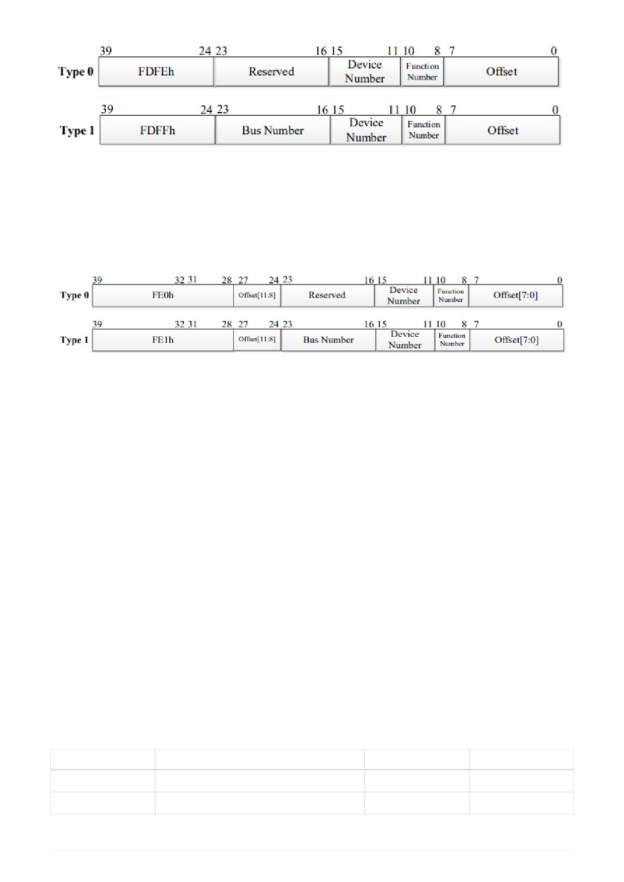
Figure 5. Standard access address of the PCI configuration
When using the HT’s reserved address space (0xFE_0000_0000 - 0xFE_1FFF_FFFF) to access bridge slices,
the maximum configuration space size per device is 4K bytes. The address [39:28] determines the
configuration header type (0xFE0 is Type0, 0xFE1 is Type1); [23:16] indicates the Bus Number; [15:11]
indicates the Device Number; [10:8] indicates the Function Number; [27:24] and [7:0] are combined to
represent the offset. The following diagram illustrates the meaning of the address segment for the CPU to
access the PCI configuration space using the HT reserved address space.
Figure 6. reserved access address of the PCI configuration
In general, it is recommended to use the HT standard configuration access space (0xFD_FE00_0000-
0xFD_FFFF_FFFF) for PCI configuration header access.
3.4. Example of Bridge Device Address Space Allocation
Access to the bridge chip devices is mainly done through the PCI MEM space. The software can assign any
access address for each device on the bridge chip within this address segment. The internal PCI devices of
the bridge chip include: GPU/DC, GMEM, PCIE, USB, SATA, GMAC, HDA/AC97, LPC, SPI, all of which can be
seen through lspci. The access addresses of these devices (except LPC) can be dynamically assigned by
software. One way of allocation is as follows: by scanning the PCI bus and reading the configuration space
of each device (PCI mode orientation) to get the size of MEM space and I/O space used by each device, the
system software allocates the appropriate size of MEM space from the address 0x40000,0000-0x7fff,fff,
and from 0x1800, 0000-0x19ff,ffff. The system software allocates the appropriate size of I/O space (PCIE
devices) from 0x40000,0000-0x7fff,ffff.
In addition to these PCI type devices, the bridge also contains some devices that are accessed using fixed
addresses, such as: interrupt controllers, HPET controllers, confbus In addition to these PCI-type devices,
the bridge also contains devices that are accessed using fixed addresses, such as: interrupt controllers,
HPET controllers, confbus configuration registers, MISC low-speed device blocks, and LPCs.
The following two tables give an example of an address allocation for a bridge chip fixed address device
and a PCI device, along with their address space size and supported access types. For the access types, B
indicates byte access (1byte), H indicates half-word access (2byte), W indicates word access (4byte), D
indicates double-word access (8byte), Q indicates 4-word access (16byte), and C indicates cacheline
access.
Table 6. Bridge piece fixed address device address space
Module
Address space
Address space size
Access type
BHW
INT
0x1000,0000-0x1000,0fff
4K
BW
HPET
0x1000,1000-0x1000,1fff
4K
26
Module
Address space
Address space size
Access type
CONF REG
0x1001,0000-0x1001,ffff
64K
BHW
BW
MISC
0x1008,0000-0x100f,ffff
512K
W
LPC REG
0x1000,2000-0x1000,2fff
4K
LPC MEM
0x1200,0000-0x13ff,ffff
32M
BHWDQC
B
LPC I/O
0x1800,0000-0x1800,ffff
64K
B
LPC TPM
0x1801,0000-0x1801,ffff
64K
Table 7. Bridge chip PCI device address space allocation example
Module
Address space
Address space size
Access type
GPU
0x5ff4,0000-0x5ff7,ffff
256K
W
W
DC
0x5ff8,0000-0x5ff8,ffff
64K
BHWDQC
Graphic Memory
0x4000,0000-0x4fff,ffff
256M
PCIE I/O
0x1802,0000-0x19ff,ffff
32M
BHW
BHW
PCIE MEM
0x6000,0000-0x7fff,ffff
512M
BHWDQC
SPI MEM
0x5e00,0000-0x5eff,ffff
16M
USB0-EHCI
0x5fd0,0000-0x5fd0,7fff
32K
W
W
USB0-OHCI
0x5fd0,8000-0x5fd0,ffff
32K
W
USB1-EHCI
0x5fd1,0000-0x5fd1,7fff
32K
USB1-OHCI
0x5fd1,8000-0x5fd1,ffff
32K
W
W
SATA0
0x5fe0,0000-0x5fe0,1fff
8K
W
SATA1
0x5fe0,2000-0x5fe0,3fff
8K
SATA2
0x5fe0,4000-0x5fe0,5fff
8K
W
W
GMAC0
0x5fe1,0000-0x5fe1,7fff
32K
W
GMAC1
0x5fe1,8000-0x5fe1,ffff
32K
HDA
0x5fe2,0000-0x5fe2,ffff
64K
BHW
W
AC97
0x5fe3,0000-0x5fe3,ffff
64K
B
SPI REG
0x5ff1,1000-0x5ff1,1fff
4K
The size of the address space of the above devices is fixed, except for PCIE MEM and Graphic Memory,
which can be changed by software.
The BIOS needs to modify the MASK value of the BAR register 2/3 of the GPU configuration header by
accessing the bridge configuration register GMEM_BAR_MASK to configure the size of Graphic Memory.
Graphic Memory size, and then the software will get the graphic memory size through PCI The software
then scans through the PCI to obtain the size of the graphics memory.
In the case of using a PCIE external discrete graphics card, the discrete graphics memory space that
comes with the discrete graphics card is located in the PCIE MEM address space and is managed as a
PCIE device.
27
Chapter 4. Bridge Configuration Register
The bridge chip sets up registers to configure certain features of the bridge chip that are not specific to a
particular interface (PCIE, USB, etc.). These registers are arranged uniformly in the bridge’s configuration
register space
(not the PCI configuration access space). The address space size of the bridge
configuration registers is 64KB, and the starting address (internal space of the bridge) is configured by the
BIOS.
The bridge chip configuration registers contain the following.
1.
Bridge chip general configuration (0x0 - 0x47f).
2. PLL configuration (0x480 - 0x4cf).
3.
PCIE controller and PHY configuration (0x580 - 0x617).
4.
SATA controller and PHY configuration (0x740 - 0x76f).
5.
Memory capacity configuration registers (0x3838 - 0x383f).
6. Bridge ID (0x3ff8 - 0x3fff).
Table 8. Bridge configuration register list
Address
Name
Read/Write
Description
Offset
0x0418
HT_ROUTE
R/W
HT Routing Configuration
R/W
0x0420
FUNC_CONFIG0
General Configuration Register 0
R/W
0x0430
FUNC_CONFIG1
General Configuration Register 1
R/W
0x0440
PAD_CONFIG
PAD Multiplexing Configuration
R/W
0x0480
PLL_0
PLL0 Configuration
0x0490
PLL_1
R/W
PLL1 Configuration
0x04a0
PLL_2
R/W
PLL2 Configuration
R/W
0x04b0
PLL_PIX_0
PLL_PIX0 Configuration
R/W
0x04c0
PLL_PIX_1
PLL_PIX1 Configuration
R/W
Device Frequency Division Configuration
0x04d0
FREQSCALE
R/W
0x0580
PCIE_F0_REG
PCIE_F0 Configuration Register
R/W
0x0590
PCIE_F0_PHY
PCIE_F0 PHY Configuration Access
Register
R/W
0x05a0
PCIE_F1_REG
PCIE_F1 Configuration Register
0x05b0
PCIE_F1_PHY
R/W
PCIE_F1 PHY Configuration Access
Register
R/W
0x0bc0
PCIE_H_REG
PCIE_H Configuration Register
R/W
0x05d0
PCIE_H_PHY_LO
PCIE_H PHY Lo Configuration Access
Register
R/W
0x05d8
PCIE_H_PHY_HI
PCIE_H PHY Hi Configuration Access
Register
0x05e0
PCIE_G0_REG
R/W
PCIE_G0 Configuration Register
28
Address
Name
Read/Write
Description
Offset
R/W
0x05f0
PCIE_G0_PHY_LO
PCIE_G0 PHY Lo Configuration Access
Register
R/W
0x05f8
PCIE_G0_PHY_HI
PCIE_G0 PHY Hi Configuration Access
Register
0x0600
PCIE_G1_REG
R/W
PCIE_G1 Configuration Register
R/W
0x0610
PCIE_G1_PHY_LO
PCIE_G1 PHY Lo Configuration Access
Register
R/W
0x0618
PCIE_G1_PHY_HI
PCIE_G1 PHY Hi Configuration Access
Register
0x0740
SATA0_REG
R/W
Configuration of SATA0
0x0748
SATA0_PHY
R/W
PHY configuration access register for SATA0
R/W
0x0750
SATA1_REG
SATA1 configuration
R/W
0x0758
SATA1_PHY
PHY configuration access register for SATA1
R/W
0x0760
SATA2_REG
SATA2 configuration
R/W
0x0768
SATA2_PHY
SATA2 PHY Configuration Access Register
0x3838
GMEM_BAR_MASK
R/W
Memory Capacity Configuration Register
0x3ff8
CHIP_ID
RO
Chip Version Number
4.1. HT clock enable and DMA routing configuration
Offset Address: 0418-041Bh
Attribute: R/W
Default value: 3h
Size: 32 bits
Table 9. Table ht clock enable
Bit Field
Name
Read/Write
Description
R/W
Reserved
31:2
Reserved
R/W
1
ht_hi_clken
HT Controller 1 Clock Enable
0: Turn off the clock
1: Turn on the clock
0
ht_lo_clken
R/W
HT Controller 0 Clock Enable
0: Turn off the clock
1: Turn on the clock
29
Offset Address: 041C-041Fh
Attribute: R/W
Default value: 000a_a800h
Size: 32 bits
This register is used to configure the routing information for the device’s DMA accesses (i.e., the
destination processor for the DMA access and the HT controller through which it passes). Since the HT bus
only supports 40-bit addresses and the processor space (and the DMA access space) supports 64-bit
addresses, the addresses need to be transformed before and after passing through the HT bus in order to
preserve the address routing information. This feature requires two supports:
1. the bridge chip stores the node number information in a certain number of bits of the HT bus address;
2. on the processor side, the node information is remapped to the processor’s node bit field using the
address translation function of the HT receive window.
The LS7A1000 implements the DMA access node number translation function, which allows the node
number in the 64-bit address space issued by the device to be automatically mapped to the HT address
space by configuring this register.
Table 10. DMA routing configuration
Bit Field
Name
Read/Write
Description
R/W
31:16
dma_dest_ht
DMA access destination node routing
configuration. There are 16 nodes, each bit
corresponds to a node number. bit31-16
correspond to DMA accesses to nodes 15-0
respectively.
1: Routed to HT controller 1
0: Routed to HT controller 0
30
Bit Field
Name
Read/Write
Description
15:13
dma_node_id_offset_ma
R/W
Address Offset of the mapped DMA access
node number in the HT address space
pped
(relative to bit32).
0: Position of the node number in the HT
address space from bit32
1: Position of the node number in the HT
address space from bit33
…
7: The location of the node number in the HT
address space starts at bit39
This register determines the maximum
address range for DMA accesses to a single
node. For example, when this register is
configured to 0 and bit`[3:0]` is not 0, the
maximum address space for DMA accesses
within a single node is 2^32=4GB.
R/W
12:8
dma_node_id_offset
The address offset (relative to bit36) where
the node number is located in the DMA
access.
R/W
Reserved
7:4
Reserved
R/W
3:0
dma_node_id_mask
Node number mask for DMA accesses. This
register determines the number of nodes
that can be accessed by device DMA access.
0 : 1 node
1 : 2 nodes
3 : 4 nodes
7 : 8 nodes
15 : 16 nodes
4.2. General Configuration Register 0
Offset Address: 0420-0423h
Attribute: R/W
Default value: CCCC_3CE0h
Size: 32 bits
This register contains configuration information related to PCIE, graphics processing unit (GPU, display
31
controller, graphics memory).
Table 11. Table General Configuration Register 0 1
Bit Field
Name
Read/Write
Description
R/W
31
pcie_g1_p1_clken
Enables the port1 clock for pcie_g1
0: Turn off the clock
1: Turn on the clock
30
pcie_g1_p0_clken
R/W
Enables the port0 clock for pcie_g1
0: Turn off the clock
1: Turn on the clock
R/W
29
pcie_g1_enable
Enable pcie_g1 controller
0: Access is disabled
1: Access is allowed
R/W
28
pcie_g1_soft_reset
Software reset of pcie_g1
0:Remove reset
1: Hold reset
27
pcie_g0_p1_clken
R/W
Enables the port1 clock for pcie_g0
0: Turn off the clock
1: Turn on the clock
R/W
26
pcie_g0_p0_clken
Enables the port0 clock for pcie_g0
0: Turn off the clock
1: Turn on the clock
25
pcie_g0_enable
R/W
Enable pcie_g0 controller
0: Access is disabled
1: Access is allowed
R/W
24
pcie_g0_soft_reset
Software reset of pcie_g0
0:Remove reset
1: Hold reset
32
Bit Field
Name
Read/Write
Description
23
pcie_h_p1_clken
R/W
Enables the port1 clock for pcie_h
0: Turn off the clock
1: Turn on the clock
R/W
22
pcie_h_p0_clken
Enables the port0 clock for pcie_h
0: Turn off the clock
1: Turn on the clock
21
pcie_h_enable
R/W
Enable pcie_h controller
0: Access is disabled
1: Access is allowed
R/W
20
pcie_h_soft_reset
Software reset of pcie_h
0:Remove reset
1: Hold reset
R/W
19
pcie_f1_p1_clken
Enables the port1 clock for pcie_f1
0: Turn off the clock
1: Turn on the clock
18
pcie_f1_p0_clken
R/W
Enables the port0 clock for pcie_f1
0: Turn off the clock
1: Turn on the clock
R/W
17
pcie_f1_enable
Enable pcie_f1 controller
0: Access is disabled
1: Access is allowed
16
pcie_f1_soft_reset
R/W
Software reset of pcie_f1
0:Remove reset
1: Hold reset
R/W
Reserved
15:14
Reserved
R/W
13
pcie_f0_p3_clken
Enables the port3 clock for pcie_f0
0: Turn off the clock
1: Turn on the clock
33
Bit Field
Name
Read/Write
Description
12
pcie_f0_p2_clken
R/W
Enables the port2 clock for pcie_f0
0: Turn off the clock
1: Turn on the clock
R/W
11
pcie_f0_p1_clken
Enables the port1 clock for pcie_f0
0: Turn off the clock
1: Turn on the clock
10
pcie_f0_p0_clken
R/W
Enables the port0 clock for pcie_f0
0: Turn off the clock
1: Turn on the clock
R/W
9
pcie_f0_enable
Enable pcie_f0 controller
0: Access is disabled
1: Access is allowed
R/W
8
pcie_f0_soft_reset
Software reset of pcie_f0
0:Remove reset
1: Hold reset
7
dc_clken
R/W
Enables clocking of dc
0: Turn off the clock
1: Turn on the clock
R/W
Enable the clock of the gpu
6
gpu_clken
0: Turn off the clock
1: Turn on the clock
5
gmem_clken
R/W
Enables the clock for gmem
0: Turn off the clock
1: Turn on the clock
R/W
Reserved
4:3
Reserved
34
Bit Field
Name
Read/Write
Description
2
pcie_clksel
R/W
Clock selection for pcie.
0: Selects the PAD input clock
1: Select the internal reference clock
If fix_pcie_clksel is 1, then the signal is
constant to 1.
1
Reserved
R/W
Reserved
R/W
Read/Writeing PCIE, graphics devices using
0
default_route_cfg0
fixed addresses. 0: Configuring device
addresses using the PCI configuration
header
1: Use fixed address to access the device
If fix_default_route is 1, then the signal is
constant to 1.
Offset Address: 0424-0427h
Attribute: R/W, RO
Default value: 0000_0000h
Size: 32 bits
Table 12. DMA routing configuration
Bit Field
Name
Read/Write
Description
31:25
Reserved
R/W
Reserved
R/W
24
disable_gmem_confspac
Disable access to the GMEM configuration
e
space
0: Access allowed
1: Access is prohibited
R/W
Reserved
23:20
Reserved
19
pcie_g1_p1_clk_ok
RO
pcie_g1 port 1 clock ready
0: No clock
1: clock normal
RO
pcie_g1 port 0 clock ready
18
pcie_g1_p0_clk_ok
0: No clock
1: clock normal
35
Bit Field
Name
Read/Write
Description
17
pcie_g0_p1_clk_ok
RO
pcie_g0 port 1 clock ready
0: No clock
1: clock normal
RO
16
pcie_g0_p0_clk_ok
pcie_g0 port 0 clock ready
0: No clock
1: clock normal
15
pcie_h_p1_clk_ok
RO
pcie_h port 1 clock ready
0: No clock
1: clock normal
RO
14
pcie_h_p0_clk_ok
pcie_h port 0 clock ready
0: No clock
1: clock normal
RO
13
pcie_f1_p1_clk_ok
pcie_f1 port 1 clock ready
0: No clock
1: clock normal
12
pcie_f1_p0_clk_ok
RO
pcie_f1 port 0 clock ready
0: No clock
1: clock normal
RO
11
pcie_f0_p0_clk_ok
pcie_f0 port 3 clock ready
0: No clock
1: clock normal
10
pcie_f0_p0_clk_ok
RO
pcie_f0 port 2 clock ready
0: No clock
1: clock normal
RO
9
pcie_f0_p0_clk_ok
pcie_f0 port 1 clock ready
0: No clock
1: clock normal
36
Bit Field
Name
Read/Write
Description
8
pcie_f0_p0_clk_ok
RO
pcie_f0 port 0 clock ready
0: No clock
1: clock normal
R/W
5
pcie_g1_uca_en
pcie_g1 uncache access acceleration
enable
0: Turn off access acceleration
1: Turn on access acceleration
4
pcie_g0_uca_en
R/W
pcie_g0 uncache access acceleration
enable
0: Turn off access acceleration
1: Turn on access acceleration
3
pcie_h_uca_en
R/W
pcie_h uncache access acceleration
enable
0: Turn off access acceleration
1: Turn on access acceleration
R/W
2
pcie_f1_uca_en
pcie_f1 uncache access acceleration
enable
0: Turn off access acceleration
1: Turn on access acceleration
1
pcie_f0_uca_en
R/W
pcie_f0 uncache access acceleration
enable
0: Turn off access acceleration
1: Turn on access acceleration
0
graphic_uca_en
R/W
GPU/DC uncache access acceleration can
be
0: Turn off access acceleration
1: Turn on access acceleration
4.3. General Configuration Register 1
Offset Address: 0430-0433h
Attribute: R/W
Default value: 00F9_BBF2h
37
Size: 32 bits
This register contains configuration information related to USB, SATA, GMAC, HDA/AC97, LPC, and SPI.
Table 13. Table general configuration register 0 2
Bit Field
Name
Read/Write
Description
R/W
31
lpc_uca_en
LPC uncache acceleration enable
0: turn off access acceleration
1: Turn on access acceleration
R/W
30
spi_uca_en
SPI uncache acceleration enable
0: Turn off access acceleration
`1: Access acceleration on
R/W
29
conf_uca_en
Configuration register uncache acceleration
enable
0: Turn off access acceleration
1: turn on access acceleration
28
misc_uca_en
R/W
Low-speed misc device uncache
acceleration enable
0: turn off access acceleration
1: turn on access acceleration
27
aud_uca_en
R/W
HDA/AC97 uncache acceleration enable
0: Turn off access acceleration
1: Turn on access acceleration
R/W
26
gmac_uca_en
gmac uncache acceleration enable
0: Turn off access acceleration
1: Turn on access acceleration
25
sata_uca_en
R/W
sata uncache acceleration enable
0: turn off access acceleration
1: Turn on access acceleration
R/W
24
usb_uca_en
usb uncache acceleration enable
0: turn off access acceleration
1: Turn on access acceleration
R/W
Reserved
23:16
Reserved
38
Bit Field
Name
Read/Write
Description
15
usb1_clken
R/W
usb1 clock enable
0: No clock
1: clock normal
R/W
14
usb1_en
usb_1 access enable
0: Access disabled
1: Access allowed
13
usb1_phy_soft_reset
R/W
usb1 PHY software reset
0:Remove reset
1: Hold reset
R/W
12
usb1_cntl_soft_reset
usb1 controller software reset
0:Remove reset
1: Hold reset
R/W
11
usb0_clken
usb0 clock enable
0: No clock
1: clock normal
10
usb0_en
R/W
usb0 access enable
0: Access disabled
1:Access allowed
R/W
9
usb0_phy_soft_reset
usb0 PHY software reset
0:Remove reset
1: Hold reset
8
usb0_cntl_soft_reset
R/W
usb0 controller software reset
0:Remove reset
1: Hold reset
R/W
7
gmac1_clken
gmac1 clock enable
0: No clock
1: clock normal
39
Bit Field
Name
Read/Write
Description
6
gmac1_sdb_flowctrl
R/W
gmac1 flow control enable
0: Flow control off
1: Flow control on
R/W
5
gmac0_clken
gmac0 clock enable
0: No clock
1: clock normal
4
gmac0_sdb_flowctrl
R/W
gmac0 flow control enable
0: Flow control off
1: Flow control on
R/W
3:2
usb_ref_clk_sel
USB PHY Reference Clock Selection
00b: Use external 12MHz crystal
10b: Use internal reference clock
R/W
1
usb_ehci_dma64_en
Enables usb EHCI 64-bit DMA address mode
0: Use 32-bit DMA address mode
1: Use 64-bit DMA address mode
0
default_route_cfg1
R/W
Use fixed addresses to access devices such
as USB, SATA, GMAC, etc.
0: Use the PCI configuration header to
configure the device address
1: Use fixed address to access the device
If fix_default_route is 1, then the signal is
constant to 1.
Note: In order to support the USB sleep-wake function, the USB reference clock must use a 12MHz external
crystal.
Offset Address: 0430-0437h
Attribute: R/W
Default value: 1209_9900h
Size: 32 bits
Table 14. Table general configuration register 0 3
40
Bit Field
Name
Read/Write
Description
28
hda_dma_64
R/W
Enables HDA64 bit DMA address mode
0: Use 32-bit DMA address mode
1: Use 64-bit DMA address mode
R/W
RTC crystal oscillator restart
27
rtc_restart
R/W
RTC Crystal Oscillator Driver Configuration
26:24
rtc_ds
19
sata2_clk_en
R/W
SATA2 clock enable
0: No clock
1: Normal clock
R/W
18
sata2_en
SATA2 access enable
0: Access disabled
1: Access allowed
16
sata2_cntl_soft_reset
R/W
SATA2 controller software reset
0: Remove reset
1: Hold reset
R/W
15
sata1_clken
SATA1 clock enable
0: No clock
1: Clock normal
R/W
14
sata1_en
SATA1 access enable
0: Access disabled
1: Access allowed
12
sata1_cntl_soft_reset
R/W
SATA1 controller software reset
0: Remove reset
`1: Hold reset
11
sata0_clken
R/W
SATA0 clock enable
0: No clock
1: Clock normal
41
Bit Field
Name
Read/Write
Description
10
sata0_en
R/W
SATA0 Access Enable
0: Access disabled
1: Access allowed
R/W
8
sata0_cntl_soft_reset
SATA0 Controller software reset
0: Remove reset
1: Hold Reset
7:1 Reserved R/W Reserved
0
lpc_en
R/W
LPC controller enable
0: Access is disabled
1: Access allowed
4.4. Pin Multiplexing Configuration Register
Offset Address: 0440-0443h
Attribute: R/W
Default value: FFFF_FFFFh
Size: 32 bits
This register contains configuration information related to pin multiplexing.
Table 15. Pin multiplexing configuration register
Bit Field
Name
Read/Write
Description
R/W
31
uart3_enable
UART operating mode selection for pin
UART_RI/DCD (when selected as UART
mode)
0: use or not is determined by bit28
1: Operates in two-wire UART3 mode
30
uart2_enable
R/W
UART operating mode selection for pin
UART_DTR/DSR (when selected as UART
mode)
0: use or not is determined by bit28
1: Operates in two-wire UART2 mode
42
Bit Field
Name
Read/Write
Description
29
uart1_enable
R/W
UART operating mode selection for pin
UART_RTS/CTS (when selected as UART
mode)
0: use or not is determined by bit28
1: Operates in two-wire UART1 mode
28
uart0_full_func
R/W
UART operating mode selection for pin
UART_TXD/RXD (when UART mode is
selected)
0: Operates in two-wire UART0 mode
1: Working in full-function UART0 mode
When bit[31:29] is not equal to 0, regardless
of the value of this bit, UART_TXD/RXD
operates in two-wire UART mode regardless
of the value of the bit.
R/W
Operating mode selection for pin
27
clkoutflex_sel
CLKOUTFLEX
0: working in GPIO mode
1: Operates in CLKOUTFLEX mode
R/W
Operating mode selection for pin
26
clkout25m_sel
CLKOUT25M
0: working in GPIO mode
1: Operating in CLKOUT25M mode
R/W
Operating mode selection for LPC pins
25
lpc_sel
(LPC_AD0-3/LPC_SERIRQ/LPC_FRAMEn)
0: working in GPIO mode
1: Working in LPC mode
24
uart_dtr_dsr_sel_i2 c
R/W
Operating mode selection for pin
UART_DTR/DSR (determined together with
bit20)
[bit24, bit20].
00b: working in GPIO mode
x1b: working in UART mode (decided by
bit[31:28] whether to work in full function
mode)
10b: working in I2C mode
43
Bit Field
Name
Read/Write
Description
23
uart_ri_dcd_sel_i2c
R/W
Operating mode selection for pin
UART_RI/DCD (determined together with
bit19)
[bit23, bit19].
00b: working in GPIO mode
x1b: working in UART mode (decided by
bit[31:28] whether to work in full function
mode)
10b: working in I2C mode
R/W
Operating mode selection for pin
22
uart_txd_rxd_sel_u
UART_TXD/RXD
art
0: working in GPIO mode
1: working in UART mode (the bit[31:28]
determines whether to work in full function
mode)
R/W
Operating mode selection for pin
21
uart_rts_cts_sel_ua
UART_RTS/CTS
rt
0: working in GPIO mode
1: working in UART mode (determined by
bit[31:28] whether to work in full function
mode)
20
uart_dtr_dsr_sel_u
R/W
Operating mode selection for pin
UART_DTR/DSR (determined together with
art
bit24)
[bit24, bit20].
00b: working in GPIO mode
x1b: working in UART mode (decided by
bit[31:28] whether to work in full function
mode)
10b: working in I2C mode
44
Bit Field
Name
Read/Write
Description
19
uart_ri_dcd_sel_uar t
R/W
Operating mode selection for pin
UART_RI/DCD (determined together with
bit23)
[bit23, bit19].
00b: working in GPIO mode
x1b: working in UART mode (decided by
bit[31:28] whether to work in full function
mode)
10b: working in I2C mode
R/W
18
usb_oc2_sel
Operating mode selection for pin USB_OC2
0: working in GPIO mode
1: Working in USB_OC mode
17
usb_oc1_sel
R/W
Operating mode selection for pin USB_OC1
0: working in GPIO mode
1: Working in USB_OC mode
R/W
Operating mode selection for pin USB_OC0
16
usb_oc0_sel
0: working in GPIO mode
1: working in USB_OC mode
15
sata2_ledn_sel
R/W
Operating mode selection for pin
SATA2_LEDn
0: working in GPIO mode
1: Operates in SATA mode
14
sata1_ledn_sel
R/W
Operating mode selection for pin
SATA1_LEDn
0: working in GPIO mode
1: Operates in SATA mode
R/W
Operating mode selection for pin
13
sata0_ledn_sel
SATA0_LEDn
0: working in GPIO mode
1: Operates in SATA mode
45
Bit Field
Name
Read/Write
Description
12:11
hda_ac97_sel
R/W
Operating mode selection for HDA pins. For
the pins
HDA_BITCLK/HDA_SYNC/HDA_RESETn/HD
A_SDO/HDA_SDI0, the operating mode is
determined by bit`[12:11]:
`00b: GPIO
mode
10b: AC97 mode
x1b: HDA mode
For pins HDA_SDI1/HDA_SDI2, the
operating mode is determined by bit[11]: 0:
GPIO mode
1: HDA mode
10
spi_sel
R/W
Operating mode selection for pin
SPI_SCK/SDI/SDO
0: Operates in GPIO mode
1: Operates in SPI mode
R/W
Operating mode selection for pin
9:8
spi_csn_23_sel_spi
SPI_CSn2/3 00b: operates in GPIOmode
x1b: working in SPI mode
10b: Operating in I2C mode
R/W
Operating mode selection for pin
7:6
spi_csn_01_sel_spi
SPI_CSn0/1 00b: Operates in GPIO mode
x1b: working in SPI mode
10b: Operating in I2C mode
5
i2c1_sel
R/W
Operating mode selection for pin
I2C1_SCL/SDA
0: working in GPIO mode
1: Working in I2C mode
R/W
Operating mode selection for pin
4
i2c0_sel
I2C0_SCL/SDA
0: working in GPIO mode
1: Working in I2C mode
46
Bit Field
Name
Read/Write
Description
3
pwm3_sel
R/W
Operating mode selection for pin PWM3
0: Operates in GPIO mode
1: Operates in PWM mode
R/W
2
pwm2_sel
Operating mode selection for pin PWM2
0: Operates in GPIO mode
1: Operates in PWM mode
1
pwm1_sel
R/W
Operating Mode Selection for Pin PWM1
0: Operates in GPIO mode
1: Operates in PWM mode
R/W
0
pwm0_sel
Operating mode selection for pin PWM0
0: Operates in GPIO mode
1: Operates in PWM mode
The multiplexing relationship between the VSB_GATEn pin and GPIO01 is configured by the internal register
(PMCON_RESUME) of the power management module, see 12.3 Register Description.
See the chip pin multiplexing table in Appendix 1 for a cross-reference to the chip pin multiplexing table.
4.5. PLL0 Configuration Register
Please refer to Section 2.5 PLL Configuration Method for the specific usage of PLL. This register is used to
set PLL0, where output clock 1 is used to generate the 125MHz clock required by the GMAC, and output
clock 0
is used to generate the controller clock for USB/SATA.
Offset Address: 0480-0483h
Attribute: R/W
Default value: 0000_0000h
Size: 32 bits
This register contains configuration information related to pin multiplexing.
Table 16. PLL0 configuration register 1
Bit Field
Name
Read/Write
Description
31:30
Reserved
R/W
Reserved
R/W
29:21
pll_loopc
PLL Multiplier
20:14
pll_div_out2
R/W
PLL output clock 2 divisions
47
Bit Field
Name
Read/Write
Description
13:7
pll_div_out1
R/W
PLL output clock 1 division
6:0
pll_div_out0
R/W
PLL output clock 0 divisions
Offset Address: 0484-0487h
Attribute: R/W
Default value: 0000_0000h
Size: 32 bits
Table 17. PLL0 configuration register 2
Bit Field
Name
Read/Write
Description
R/W
Reserved
31:14
Reserved
13
pll_pd
R/W
PLL powerdown
R/W
PLL internal bypass
12
pll_bypass
R/W
11
set_pll_param
Set PLL configuration parameters
R/W
10
sel_pll_out2
Select PLL output clock 2
R/W
9
sel_pll_out1
Select PLL output clock 1
R/W
8
sel_pll_out0
Select PLL Output Clock 0
7
pll_locked
RO
PLL Lock
6:0
pll_div_ref
R/W
PLL Input Frequency Division Number
4.6. PLL1 Configuration Register
Please refer to Section 2.5 PLL Configuration Method for the specific usage of PLL.
This register is used to set PLL1, where output clock 2 is used to generate the GPU clock, output clock 1 is
used to generate the GMEM clock, and output clock 0 is used to generate the DC clock.
Offset Address: 0490-0493h
Attribute: R/W
Default value: 0000_0000h
Size: 32 bits
Table 18. PLL1 configuration register 1
Bit Field
Name
Read/Write
Description
31:30
Reserved
R/W
Reserved
R/W
29:21
pll_loopc
PLL Multiplier
20:14
pll_div_out2
R/W
PLL output clock 2 divisions
48
Bit Field
Name
Read/Write
Description
13:7
pll_div_out1
R/W
PLL output clock 1 division
6:0
pll_div_out0
R/W
PLL output clock 0 divisions
Offset Address: 0494-0497h
Attribute: R/W
Default value: 0000_0000h
Size: 32 bits
Table 19. PLL1 configuration register 2
Bit Field
Name
Read/Write
Description
R/W
Reserved
31:14
Reserved
13
pll_pd
R/W
PLL powerdown
12
pll_bypass
R/W
PLL internal bypass
R/W
11
set_pll_param
Set PLL configuration parameters
R/W
10
sel_pll_out2
Select PLL output clock 2
R/W
9
sel_pll_out1
Select PLL output clock 1
R/W
8
sel_pll_out0
Select PLL Output Clock 0
7
pll_locked
RO
PLL Lock
6:0
pll_div_ref
R/W
PLL Input Frequency Division Number
4.7. PLL2 Configuration Register
Please refer to Section 2.5 PLL Configuration Method for the specific usage of PLL. This register is used to
set PLL2, where output clock 2 is used to generate the CLKOUTFLEX clock, output clock 1 is used to
generate the internal bus clock, and output clock 0 is used to generate the 24MHz bitclk clock required by
the HDA.
Output Clock 1 is used to generate the internal bus clock, and Output Clock 0 is used to generate the
24MHz bitclk clock required by the HDA.
Address Offset: 04A0-04A3h
Attribute: R/W
Default value: 0000_0000h
Size: 32 bits
Table 20. Pll2 configuration register 1
Bit Field
Name
Read/Write
Description
31:30
Reserved
R/W
Reserved
R/W
PLL Multiplier
29:21
pll_loopc
49
Bit Field
Name
Read/Write
Description
20:14
pll_div_out2
R/W
PLL output clock 2 divisions
13:7
pll_div_out1
R/W
PLL output clock 1 division
R/W
6:0
pll_div_out0
PLL output clock 0 divisions
Address Offset: 04A4-04A7h
Attribute: R/W
Default value: 0000_0000h
Size: 32 bits
Table 21. Pll2 configuration register 2
Bit Field
Name
Read/Write
Description
R/W
Reserved
31:14
Reserved
13
pll_pd
R/W
PLL powerdown
R/W
PLL internal bypass
12
pll_bypass
R/W
Set PLL configuration parameters
11
set_pll_param
10
sel_pll_out2
R/W
Select PLL output clock 2
R/W
9
sel_pll_out1
Select PLL output clock 1
R/W
8
sel_pll_out0
Select PLL Output Clock 0
RO
PLL Lock
7
pll_locked
R/W
PLL Input Frequency Division Number
6:0
pll_div_ref
4.8. PLL_PIX_0 Configuration Register
Refer to Section 2.5 PLL Configuration Methods for the specific usage of the PLL.
This register is used to set PLL_PIX_0, where output clock 0 is used to generate the PIX0 clock.
Address Offset: 04B0-04B3h
Attribute: R/W
Default value: 0000_0000h
Size: 32 bits
Table 22. Pll pix 0 configuration register 1
Bit Field
Name
Read/Write
Description
R/W
Reserved
31:30
Reserved
R/W
PLL Multiplier
29:21
pll_loopc
20:7
Reserved
R/W
Reserved
50
Bit Field
Name
Read/Write
Description
6:0
pll_div_out0
R/W
PLL Output Clock 0 Divider
Address Offset: 04B4-04B7h
Attribute: R/W
Default value: 0000_0000h
Size: 32 bits
Table 23. Pll pix 0 configuration register 2
Bit Field
Name
Read/Write
Description
31:14
Reserved
R/W
Reserved
R/W
PLL powerdown
13
pll_pd
R/W
PLL internal bypass
12
pll_bypass
11
set_pll_param
R/W
Set PLL configuration parameters
R/W
Reserved
10:9
Reserved
R/W
8
sel_pll_out0
Select PLL output clock 0
RO
PLL Lock
7
pll_locked
R/W
Number of PLL input divisions
6:0
pll_div_ref
4.9. PLL_PIX_1 Configuration Register
Refer to Section 2.5 PLL Configuration Methods for the specific usage of the PLL. This register is used to
set PLL_PIX_1, where output clock 0 is used to generate the PIX1 clock.
Address Offset: 04C0-04C3h
Attribute: R/W
Default value: 0000_0000h
Size: 32 bits
Table 24. PLL_PIX_1 Configuration Register 1
Bit Field
Name
Read/Write
Description
R/W
Reserved
31:30
Reserved
R/W
PLL Multiplier
29:21
pll_loopc
20:7
Reserved
R/W
Reserved
6:0
pll_div_out0
R/W
PLL Output Clock 0 Divider
Address Offset: 04C4-04C7h
Attribute: R/W
51
Default value: 0000_0000h
Size: 32 bits
Table 25. PLL_PIX_1 Configuration Register 2
Bit Field
Name
Read/Write
Description
R/W
Reserved
31:14
Reserved
R/W
PLL powerdown
13
pll_pd
12
pll_bypass
R/W
PLL internal bypass
R/W
Set PLL configuration parameters
11
set_pll_param
R/W
Reserved
10:9
Reserved
8
sel_pll_out0
R/W
Select PLL output clock 0
7
pll_locked
RO
PLL lockout
6:0
pll_div_ref
R/W
Number of PLL input divisions
4.10. PCIE_F0 PHY Configuration Register
This set of registers contains the control signals for PCIE_F0 PHY.
Address Offset: 0588-058Bh
Attribute: R/W,RO
Default value: 0006_0000h
Size: 32 bits
Table 26. Pcie f0 phy configuration register
Bit Field
Name
Read/Write
Description
R/W
Enable software to configure the operating
27
cfg_x4_mode_en
mode of PCIE_F0 0: the operating mode is
determined by the hardware pin 1: The
operating mode is determined by the
software configuration (bit26)
R/W
Software configuration of PCIE_F0 operating
26
cfg_x4_mode
modes
0: working in x1 mode
1: working in x4 mode
24
phy_powerdown
R/W
Set PHY into low-power mode
4.11. PCIE_F0 PHY Access Configuration Register
This group of registers is used to control the configuration access operation that generates the PCIE_F0
PHY internal control register. This register controls the 4 data links of PCIE_F0.
52
Address Offset: 0590-0593h
Attribute: R/W
Default value: 0000_0000h
Size: 32 bits
Table 27. PCIE_F0 PHY Access Configuration Register 1
Bit Field
Name
Read/Write
Description
31:16
phy_cfg_data
R/W
PHY configuration reads and writes data.In
the write operation, the data is written to this
register before the write operation is
executed; in the read operation, the read
data returned from PHY is stored to this
register.
R/W
PHY configures the address.
15:0
phy_cfg_addr
Address Offset: 0594-0597h
Attribute: R/W,
Default value: 0000_0000h
Size: 32 bits
Table 28. PCIE_F0 PHY Access Configuration Register 2
Bit Field
Name
Read/Write
Description
31:7
Reserved
R/W
Reserved
R/W
PHY Configuration Reset, High Active
6
phy_cfg_reset
RO
PHY Configuration Status Machine Status
5:3
phy_cfg_state
Indication
2
phy_cfg_done
R/W
PHY One access completion indicates the
completion of reading and writing to PHY.
Write completion indicates that the write
data has been written to the PHY internal
register, and read completion indicates that
the read data has been returned to the to the
phy_cfg_data register
R/W
0 - Read and write to this set of registers will
1
phy_cfg_disable
trigger PHY configuration access operation
1 - Read or write to this set of registers does
not trigger PHY configuration access
operation, only a simple register read or
write
0
phy_cfg_R/W
R/W
Start a read operation or a write operation.
0: Read operation
1: Write operation
53
4.12. PCIE_F1 PHY Configuration Register
This set of registers contains the control signals for PCIE_F1 PHY.
Address Offset: 05A8-05ABh
Attribute: R/W,RO
Default value: 0006_0000h
Size: 32 bits
Table 29. PCIE_F1 PHY Configuration Register 1
Bit Field
Name
Read/Write
Description
R/W
Enable software to configure the operating
27
cfg_x4_mode_en
mode of PCIE_F1
0: the operating mode is determined by the
hardware pin
1: The operating mode is determined by the
software configuration (bit26)
R/W
Software configuration of PCIE_F1 operating
26
cfg_x4_mode
modes
0: working in x1 mode
1: working in x4 mode
24
phy_powerdown
R/W
Set PHY into low-power mode
4.13. PCIE_F1 PHY Access Configuration Register
This group of registers is used to control the configuration access operation that generates the PCIE_F1
PHY internal control register. This register controls the 4 data links of PCIE_F1.
Address Offset: 05B0-05B3h
Attribute: R/W
Default value: 0000_0000h
Size: 32 bits
Table 30. pcie f1 phy access configuration register 1
Bit Field
Name
Read/Write
Description
31:16
phy_cfg_data
R/W
PHY configuration reads and writes data. In
the write operation, the data is written to this
register first, and then the write operation is
performed. In the read operation, the read
data returned from PHY is stored into this
register.
54
Bit Field
Name
Read/Write
Description
15:0
phy_cfg_addr
R/W
PHY configuration address
Address Offset: 05B4-05B7h
Attribute: R/W
Default value: 0000_0000h
Size: 32 bits
Table 31. pcie f1 phy access configuration register 2
Bit Field
Name
Read/Write
Description
R/W
Reserved
31:7
Reserved
R/W
6
phy_cfg_reset
PHY Configuration Reset, High Active
RO
5:3
phy_cfg_state
PHY Configuration Status Machine Status
Indication
R/W
2
phy_cfg_done
The completion of one access to PHY
indicates the completion of reading and
writing to PHY. Write completion indicates
that the written data has been written to the
PHY internal register, and read completion
indicates that the read data has been
returned to the phy_cfg_data register
R/W
1
phy_cfg_disable
0 - Read or write to this group of registers
will trigger the PHY configuration access
operation
1 - Read or write to this set of registers does
not trigger PHY configuration access
operation, only a simple register read or
write
R/W
Start a read operation or a write operation.
0
phy_cfg_R/W
0: Read operation
1: Write operation
4.14. PCIE_H PHY Configuration Register
This group of registers contains the control signals for PCIE_H PHY.
Address Offset: 05C8-05CBh
Attribute: R/W,RO
Default value: 0006_0000h
Size: 32 bits
55
Table 32. Pcie h phy configuration register
Bit Field
Name
Read/Write
Description
27
cfg_x4_mode_en
R/W
Enable software to configure the operating
mode of PCIE_H
0: the operating mode is determined by the
hardware pins
1: The operating mode is determined by the
software configuration (bit26)
R/W
26
cfg_x4_mode
Software configuration of PCIE_H operating
modes
0: working in x8 mode
1: working in x4 mode
R/W
25
phy_powerdown_hi
Set the high four bits of PHY to enter the low-
power mode
R/W
24
phy_powerdown_lo
Set PHY low four bits to enter low-power
mode
4.15. PCIE_H PHY LO Access Configuration Register
This group of registers is used to control the configuration access operation that generates the PCIE_H
PHY LO internal control register. This register controls the the lower 4 data links (lane0-3) of PCIE_H.
Address Offset: 05D0-05D3h
Attribute: R/W
Default value: 0000_0000h
Size: 32 bits
Table 33. Pcie h phy lo access configuration register 1
Bit Field
Name
Read/Write
Description
31:16
phy_cfg_data
R/W
PHY configuration reads and writes data. In
the write operation, the data is written to this
register first, and then the write operation is
performed. In the read operation, the read
data returned from PHY is stored into this
register.
R/W
PHY Configuration Address
15:0
phy_cfg_addr
Address Offset: 05D4-05D7h
Attribute: R/W,
Default value: 0000_0000h
Size: 32 bits
56