Loongson 7A1000 Bridge User Manual. Loongson Technology Corporation Limited Version 2.00 - page 1
Loongson 7A1000 Bridge User Manual
Loongson Technology Corporation Limited
Version 2.00
Table of Contents
List of Figures
1
List of Tables
2
About this manual
10
Copyright Statement
10
Disclaimer
10
Loongson Technology Corporation Limited
10
Reading Guide
10
Translator’s Note
10
License
10
Contributors
10
1. Introduction
12
1.1. Introduction to this Manual
12
1.1.1. Contents of the Chapters
12
1.1.2. Conventions of this Manual
13
1.2. Overview of the Bridge
13
1.3. Main Functions of the Bridge
14
1.4. Structure of the Bridge
15
2. Bridge and System Clock
17
2.1. Bridge Clock
17
2.2. Clock-related Configuration Pins
18
2.3. Description of Clock Function
18
2.4. Description of PLL Function
19
2.5. Configuration Method of PLL
20
3. Address Space
22
3.1. Overview of Loongson 3 and Loongson 7A Address Space
22
3.2. PCI Devices and Functions
24
3.3. Access Address of the PCI Configuration
25
3.4. Example of Bridge Device Address Space Allocation
26
4. Bridge Configuration Register
28
4.1. HT clock enable and DMA routing configuration
29
4.2. General Configuration Register 0
31
4.3. General Configuration Register 1
37
4.4. Pin Multiplexing Configuration Register
42
47
4.5. PLL0 Configuration Register
48
4.6. PLL1 Configuration Register
49
4.7. PLL2 Configuration Register
. . . . . . . . . . . . . . . . . . . . . . . . . . . . . . . . . . . . . . . . . . . . . . . . . . . . . . 50
4.8. PLL_PIX_0 Configuration Register
. . . . . . . . . . . . . . . . . . . . . . . . . . . . . . . . . . . . . . . . . . . . . . . . . . . . . . 51
4.9. PLL_PIX_1 Configuration Register
. . . . . . . . . . . . . . . . . . . . . . . . . . . . . . . . . . . . . . . . . . . . . . . . . . 52
4.10. PCIE_F0 PHY Configuration Register
. . . . . . . . . . . . . . . . . . . . . . . . . . . . . . . . . . . . . . . . . . . 52
4.11. PCIE_F0 PHY Access Configuration Register
. . . . . . . . . . . . . . . . . . . . . . . . . . . . . . . . . . . . . . . . . . . . . . . . . . 54
4.12. PCIE_F1 PHY Configuration Register
. . . . . . . . . . . . . . . . . . . . . . . . . . . . . . . . . . . . . . . . . . . 54
4.13. PCIE_F1 PHY Access Configuration Register
55
4.14. PCIE_H PHY Configuration Register
. . . . . . . . . . . . . . . . . . . . . . . . . . . . . . . . . . . . . . . . . 56
4.15. PCIE_H PHY LO Access Configuration Register
. . . . . . . . . . . . . . . . . . . . . . . . . . . . . . . . . . . . . . . . . 57
4.16. PCIE_H PHY HI Access Configuration Register
4.17. PCIE_G0 PHY Configuration Register
58
. . . . . . . . . . . . . . . . . . . . . . . . . . . . . . . . . . . . . . . . 59
4.18. PCIE_G0 PHY LO Access Configuration Register
. . . . . . . . . . . . . . . . . . . . . . . . . . . . . . . . . . . . . . . . 60
4.19. PCIE_G0 PHY HI Access Configuration Register
. . . . . . . . . . . . . . . . . . . . . . . . . . . . . . . . . . . . . . . . . . . . . . . . . . 61
4.20. PCIE_G1 PHY Configuration Register
. . . . . . . . . . . . . . . . . . . . . . . . . . . . . . . . . . . . . . . . 62
4.21. PCIE_G1 PHY LO Access Configuration Register
. . . . . . . . . . . . . . . . . . . . . . . . . . . . . . . . . . . . . . . . 63
4.22. PCIE_G1 PHY HI Access Configuration Register
64
4.23. SATA0 PHY Configuration Register
. . . . . . . . . . . . . . . . . . . . . . . . . . . . . . . . . . . . . . . . . . . . . . 65
4.24. SATA0 PHY Access Configuration Register
66
4.25. SATA1 PHY Configuration Register
. . . . . . . . . . . . . . . . . . . . . . . . . . . . . . . . . . . . . . . . . . . . . . 67
4.26. SATA1 PHY Access Configuration Register
68
4.27. SATA2 PHY Configuration Register
. . . . . . . . . . . . . . . . . . . . . . . . . . . . . . . . . . . . . . . . . . . . . . 69
4.28. SATA2 PHY Access Configuration Register
4.29. Memory Capacity Configuration Register
70
4.30. Bridge Identity register
71
5. Interrupt Controller
72
5.1. Interrupt Source Assignment
73
5.2. Description of Interrupt-related Registers
74
5.3. Device Interrupt Types
94
5.4. Interrupt Distribution Modes
94
5.5. Detailed Description of Interrupt Handling Process
95
6. HPET Controller
97
6.1. Access Address
97
6.2. Description of Registers
97
7. HT Controller
103
7.1. HT User Guide
103
7.1.1. HT Working Mode
103
7.1.2. HT Address Space
103
7.2. HT Configuration Register
104
8. MISC Low-speed Devices
115
8.1. MISC Low-speed Devices Configuration Register
115
8.2. Internal Device Address Routing
115
9. UART Controller
116
9.1. Access Address
116
9.2. Description of Registers
116
10. I2C Controller
123
10.1. Access Address and Pin Multiplexing
123
10.2. Description of I2C Controller Register
123
11. PWM Controller
127
11.1. Access Address and Pin Multiplexing
127
11.2. Description of Registers
127
11.3. Description of Functions
129
11.3.1. Pulse Width Modulation Function
129
11.3.2. Pulse Measurement Function
129
11.3.3. Anti Dead Zones Function
130
12. Power Management Module (ACPI Support)
131
12.1. Access Address
131
12.2. Power Level
131
12.3. Description of Registers
131
13. RTC
142
13.1. Access Address
142
13.2. Description of Registers
142
. . . . . . . . . . . . . . . . . . . . . . . . . . . . . . . . . . . . . . . . . . . . . . . . . . . . . . . . . . . . . . . 143
13.2.1. SYS_TOYWRITE0
. . . . . . . . . . . . . . . . . . . . . . . . . . . . . . . . . . . . . . . . . . . . . . . . . . . . . . . . . . . . . . . 143
13.2.2. SYS_TOYWRITE1
. . . . . . . . . . . . . . . . . . . . . . . . . . . . . . . . . . . . . . . . . . . . . . . . . . . . . . . . . . . . . . . . 143
13.2.3. SYS_TOYREAD0
. . . . . . . . . . . . . . . . . . . . . . . . . . . . . . . . . . . . . . . . . . . . . . . . . . . . . . . . . . . . . . . . 144
13.2.4. SYS_TOYREAD1
. . . . . . . . . . . . . . . . . . . . . . . . . . . . . . . . . . . . . . . . . . . . . . . . . . . . . . . . . . . . . . . 144
13.2.5. SYS_TOYMATCH0
. . . . . . . . . . . . . . . . . . . . . . . . . . . . . . . . . . . . . . . . . . . . . . . . . . . . . . . . . . . . . . . 145
13.2.6. SYS_TOYMATCH1
. . . . . . . . . . . . . . . . . . . . . . . . . . . . . . . . . . . . . . . . . . . . . . . . . . . . . . . . . . . . . . . 145
13.2.7. SYS_TOYMATCH2
. . . . . . . . . . . . . . . . . . . . . . . . . . . . . . . . . . . . . . . . . . . . . . . . . . . . . . . . . . . . . . . . . 145
13.2.8. SYS_RTCCTRL
. . . . . . . . . . . . . . . . . . . . . . . . . . . . . . . . . . . . . . . . . . . . . . . . . . . . . . . . . . . . . . . . 147
13.2.9. SYS_RTCWRITE
. . . . . . . . . . . . . . . . . . . . . . . . . . . . . . . . . . . . . . . . . . . . . . . . . . . . . . . . . . . . . . . . 147
13.2.10. SYS_RTCREAD
. . . . . . . . . . . . . . . . . . . . . . . . . . . . . . . . . . . . . . . . . . . . . . . . . . . . . . . . . . . . . . 147
13.2.11. SYS_RTCMATCH0
. . . . . . . . . . . . . . . . . . . . . . . . . . . . . . . . . . . . . . . . . . . . . . . . . . . . . . . . . . . . . . 147
13.2.12. SYS_RTCMATCH1
. . . . . . . . . . . . . . . . . . . . . . . . . . . . . . . . . . . . . . . . . . . . . . . . . . . . . . . . . . . . . . 148
13.2.13. SYS_RTCMATCH2
14. GPIO
149
14.1. Access Address
149
14.2. Description of Registers
150
. . . . . . . . . . . . . . . . . . . . . . . . . . . . . . . . . . . . . . . . . . . . . . . . . . . . . . . . . 153
15. GMAC Controller (D3:F0, D3:F1)
. . . . . . . . . . . . . . . . . . . . . . . . . . . . . . . . . . . . . . . . . . 153
15.1. GMAC Configuration Register (D3:F0, D3:F1)
. . . . . . . . . . . . . . . . . . . . . . . . . . . . . . . . . . . . . . . . . . . . . . . . . . . . . . 155
16. USB Controller (D4:F0/1, D5:F0/1)
16.1. EHCI Controller
155
155
16.1.1. EHCI Configuration Register (D4:F1, D5:F1)
16.2. OHCI Controller
157
. . . . . . . . . . . . . . . . . . . . . . . . . . . . . . . . . . . . . . . 157
16.2.1. OHCI Configuration Register (D4:F0, D5:F0)
. . . . . . . . . . . . . . . . . . . . . . . . . . . . . . . . . . . . . . . . . . . . . . . . . . . . . . . . . . . . . 160
17. Graphics Processor (D6:F0)
160
17.1. GPU Configuration Register (D6:F0)
17.2. DDR3 Memory Interface
163
. . . . . . . . . . . . . . . . . . . . . . . . . . . . . . . . . . . . . . . . . . . . . . . . . . . . . . . . . . . . . . . 164
18. Display Controller (D6:F1)
. . . . . . . . . . . . . . . . . . . . . . . . . . . . . . . . . . . . . . . . . . . . . . . . . . . . 164
18.1. DC Configuration Register (D6:F1)
18.2. DC Control Register
166
18.2.1. Display Detection Register
166
. . . . . . . . . . . . . . . . . . . . . . . . . . . . . . . . . . . . . . . . . . . . . . . . . . . . . . . . . . . . . . . . . 168
19. HDA Controller (D7:F0)
168
19.1. HDA Configuration Register (D7:F0)
19.2. Description of HDA Control Register
170
171
20. AC97 Controller (D7:F1)
171
20.1. AC97 Configuration Register (D7:F1)
20.2. AC97 Controller Register
173
20.3. DMA Controller
178
20.3.1. Description of DMA Controller Structure
178
20.3.2. DMA Descriptor
178
183
21. SATA Controller (D8:F0/1/2)
21.1. SATA Configuration Register (D8:F0/1/2)
183
21.2. Description of SATA Control Register
185
22. PCIE Controller (D9:F0, D10:F0, D11:F0, D12:F0, D13:F0, D14:F0, D15:F0, D16:F0, D17:F0,
D18:F0, D19:F0, D20:F0)
187
22.1. PCI Configuration Register
188
22.2. Address Space Division
190
22.3. Special Notes
191
. . . . . . . . . . . . . . . . . . . . . . . . . . . . . . . . . . . . . . . . . . . . . . . . . . . . . . . . . . . . . . . . . 192
23. SPI Controller (D22:F0)
. . . . . . . . . . . . . . . . . . . . . . . . . . . . . . . . . . . . . . . . . . . . . . . . . . 192
23.1. SPI Configuration Register (D22:F0)
23.2. SPI Control Register
194
23.3. SPI Software Programming Guide
198
200
24. LPC Controller (D23:F0)
200
24.1. LPC Configuration Register (D23:F0)
24.2. LPC Access Address
202
24.3. LPC Interrupt
202
24.4. LPC Control Register
203
Appendix A: Table of Pin Multiplexing
206
Appendix B: Notes on the Use of the Software
208
List of Figures
• Structure of the Bridge
• Structure of bridge clock
• Structure of PLL
• Example of address space division for Loongson 3 processor + Loongson 7A bridge
• Standard access address of the PCI configuration
• reserved access address of the PCI configuration
• Schematic of the interrupt system of 3A + 7A
• Anti dead zones function
1
List of Tables
•
Bridge clock
•
Birge clock output
•
Bridge chip clock-related configuration pins and descriptions
•
PLL-related configuration signal description table
•
Configuration header access correspondence for each device
•
Bridge piece fixed address device address space
•
Bridge chip PCI device address space allocation example
•
Bridge configuration register list
•
Table ht clock enable
•
DMA routing configuration
•
Table General Configuration Register 0 1
•
DMA routing configuration
•
Table general configuration register 0 2
•
Table general configuration register 0 3
•
Pin multiplexing configuration register
•
PLL0 configuration register 1
•
PLL0 configuration register 2
•
PLL1 configuration register 1
•
PLL1 configuration register 2
•
Pll2 configuration register 1
•
Pll2 configuration register 2
•
Pll pix 0 configuration register 1
•
Pll pix 0 configuration register 2
•
PLL_PIX_1 Configuration Register 1
•
PLL_PIX_1 Configuration Register 2
•
Pcie f0 phy configuration register
•
PCIE_F0 PHY Access Configuration Register 1
•
PCIE_F0 PHY Access Configuration Register 2
•
PCIE_F1 PHY Configuration Register 1
•
pcie f1 phy access configuration register 1
•
pcie f1 phy access configuration register 2
•
Pcie h phy configuration register
•
Pcie h phy lo access configuration register 1
•
Pcie h phy lo access configuration register 2
•
Pcie h phy hi access configuration register 1
•
Pcie h phy hi access configuration register 2
•
Pcie g0 phy configuration register
•
Pcie g0 phy lo access configuration register 1
•
Pcie g0 phy lo access configuration register 2
2
•
Pcie g0 phy hi access configuration register 1
•
Pcie g0 phy hi access configuration register 2
•
PCIE_G1 PHY configuration register
•
PCIE_G1 PHY LO access configuration register 1
•
PCIE_G1 PHY LO access configuration register 2
•
PCIE_G1 PHY HI access configuration register 1
•
PCIE_G1 PHY HI access configuration register 2
•
SATA0 PHY Configuration Register 1
•
SATA0 PHY Configuration Register 2
•
SATA0 PHY Access Configuration Register 1
•
SATA0 PHY Access Configuration Register 2
•
SATA1 PHY Configuration Register 1
•
SATA1 PHY Configuration Register 2
•
SATA1 PHY Access Configuration Register 1
•
SATA1 PHY Access Configuration Register 2
•
SATA2 PHY Configuration Register 1
•
SATA2 PHY Configuration Register 2
•
SATA2 PHY Access Configuration Register 1
•
SATA2 PHY Access Configuration Register 2
•
Memory capacity configuration register 1
•
Memory capacity configuration register 2
•
Bridge Identity register 3
•
Bridge Identity register 4
•
Bridge chip interrupt controller interrupt source assignment
•
Interrupt control and status registers
•
Interrupt register address distribution
•
Interrupt controller identification register 1
•
Interrupt controller identification register 2
•
Interrupt mask register 1
•
Interrupt mask register 2
•
HT interrupt message packet enable register 1
•
HT interrupt message packet enable register 2
•
Interrupt trigger control register 1
•
Interrupt trigger control register 2
•
Interrupt clear register 1
•
Interrupt clear register 2
•
INT_AUTO_CTRL0 register 1
•
INT_AUTO_CTRL0 register 2
•
INT_AUTO_CTRL1 register 1
•
INT_AUTO_CTRL1 register 2
•
Interrupt routing configuration register 1
3
•
Interrupt routing configuration register 2
•
Interrupt routing configuration register 3
•
Interrupt routing configuration register 4
•
Interrupt routing configuration register 5
•
Interrupt routing configuration register 6
•
Interrupt routing configuration register 7
•
Interrupt routing configuration register 8
•
Interrupt routing configuration register 9
•
Interrupt routing configuration register 10
•
Interrupt routing configuration register 11
•
Interrupt routing configuration register 12
•
Interrupt routing configuration register 13
•
Interrupt routing configuration register 14
•
Interrupt routing configuration register 15
•
Interrupt routing configuration register 16
•
HT message packet interrupt vector configuration register 1
•
HT message packet interrupt vector configuration register 2
•
HT message packet interrupt vector configuration register 3
•
HT message packet interrupt vector configuration register 4
•
HT message packet interrupt vector configuration register 5
•
HT message packet interrupt vector configuration register 6
•
HT message packet interrupt vector configuration register 7
•
HT message packet interrupt vector configuration register 8
•
HT message packet interrupt vector configuration register 9
•
HT message packet interrupt vector configuration register 10
•
HT message packet interrupt vector configuration register 11
•
HT message packet interrupt vector configuration register 12
•
HT message packet interrupt vector configuration register 13
•
HT message packet interrupt vector configuration register 14
•
HT message packet interrupt vector configuration register 15
•
HT message packet interrupt vector configuration register 16
•
HT message packet interrupt vector configuration register 17
•
HT message packet interrupt vector configuration register 18
•
Interrupts routed to INTn1 are in the service status segister 1
•
Interrupts routed to INTn1 are in the service status segister 2
•
Interrupt request register 1
•
Interrupt request register 2
•
Interrupt in service status register 1
•
Interrupt in service status register 2
•
Interrupt level trigger polarity register 1
•
Interrupt level trigger polarity register 2
4
•
Access address
•
HPET register list
•
General capabilities and id register
•
General configuaration register
•
General interrupt status register
•
Main counter value register
•
Timer 0 configuration and capabilities registe
•
Timer 0 comparator value register
•
HT configuration register
•
BCTRL-HT bridge control register
•
DIDCMD-device ID command register
•
LKSC0-Link status control register 0
•
LKWDSC0-Link data width status and control register
•
LKFREQCFG0-Link frequency configuration register 1
•
LKFREQCFG0-Link frequency configuration register 2
•
RXWIN-receive address window
•
RXWIN0-Receive window register 0
•
RXWIN1-Receive window register 1
•
RXWIN2-Receive window register 2
•
RXWIN3-Receive window register 3
•
RXWIN4-Receive window register 4
•
TXPOSTWIN - quick send window
•
TXPOSTWIN0-Quick send window register 0
•
TXPOSTWIN1-Quick send window register 1
•
RXP2PWIN-P2P receive window
•
RXP2PWIN0-P2P receive window 0
•
RXP2PWIN1-P2P receive window 1
•
Htpllctrl-ht pll control register
•
MISC Low-speed device address routing and access types
•
MISC Low-speed device address routing
•
UART function reuse
•
Module physical address composition
•
UART function reuse
•
Interrupt enable register (IER)
•
Interrupt identification register (IIR)
•
Interrupt control menu
•
FIFO control register (FCR)
•
Line control register (LCR)
•
MODEM control register (MCR)
•
Line status register (LSR)
•
MODEM status register (MSR)
5
•
Frequency divider latch 1
•
Frequency divider latch 2
•
The physical address composition of the I2C module internal registers
•
Frequency division latch low-order byte register
•
Frequency division latch high-order byte register
•
Control register
•
Transport data register
•
Receive data register
•
Command control register
•
State register
•
The physical address composition of the PWM controller internal registers
•
List of PWM registers
•
The physical address composition of the ACPI controller internal registers
•
Description of ACPI status
•
SOC general PM configuration register
•
RESUME general PM configuration register
•
RTC general PM configuration register
•
Power Management 1 Status Register
•
Power management 1 enable register
•
Power management 1 control register
•
Power management 1 timer
•
General purpose event0 status register
•
General purpose event0 enable register
•
Reset control register
•
Watch dog set register
•
Watch dog timer register
•
General RTC register 1
•
General RTC register 2
•
The physical address composition of the RTC module internal registers
•
List of RTC registers
•
SYS_TOYWRITE0
•
SYS_TOYWRITE1
•
SYS_TOYREAD0
•
SYS_TOYREAD1
•
SYS_TOYMATCH0
•
SYS_TOYMATCH1
•
SYS_TOYMATCH2
•
SYS_RTCCTRL
•
SYS_RTCWRITE
6
•
SYS_RTCREAD
•
SYS_RTCMATCH0
•
SYS_RTCMATCH1
•
SYS_RTCMATCH2
•
GPIO control register
•
The physical address composition of the GPIO module internal registers
•
Address of GPIO bit control configuration register
•
Address of GPIO byte control configuration register
•
GPIO direction control
•
GPIO direction control
•
GPIO output
•
GPIO output
•
GPIO input
•
GPIO input
•
GPIO interrupt enable
•
GPIO interrupt enable
•
GMAC controller configuration registers
•
PCI command register
•
Control base address register
•
Control base address register
•
USB-EHCI controller configuration registers
•
PCI command register
•
Control base address register
•
Control base address register
•
USB-OHCI controller configuration registers
•
PCI command register
•
Control base address register
•
Control base address register
•
GPU controller configuration registers
•
PCI command register
•
Control base address register
•
Control base address register
•
Video memory base address register
•
Video memory base address register
•
Reserved window base address register
•
Reserved window base address register
•
DC controller configuration registers
•
PCI command register
•
Control base address register
•
Control base address register
7
•
Correspondence between the I2C pins of the DVO and the control registers
•
DVO’s I2C pin control register address
•
HDA controller configuration registers
•
PCI command register
•
Control base address register
•
Control base address register
•
AC97 controller configuration registers
•
PCI command register
•
Control base address register
•
Control base address register
•
List of AC97 control registers
•
CSR register
•
OCC register
•
ICC register
•
Description of the sound channel format
•
Codec register access command
•
Interrupt Status Register/Interrupt Mask Register
•
Interrupt status/clear register
•
OC interrupt clear register
•
IC interrupt clear register
•
CODEC WRITE interrupt clear register
•
CODEC READ interrupt clear register
•
DMA command register
•
DMA_ORDER_ADDR_LOW
•
DMA_SADDR
•
DMA_DADDR
•
DMA_LENGTH
•
DMA_STEP_LENGTH
•
DMA_STEP_TIMES
•
DMA_CMD
•
DMA write state
•
DMA read state
•
DMA_ORDER_ADDR_HIGH
•
DMA_SADDR_HIGH
•
SATA controller configuration registers
•
PCI command register
•
Control base address register
•
Control base address register
8
•
List of SATA control registers
•
Configuration methods and control ports supported by PCIE_F0
•
Configuration methods and control ports supported by PCIE_F1
•
PCIE controller configuration registers
•
Device identity register
•
Table of DID of PCIE port
•
SPI controller configuration registers
•
PCI command register
•
Control base address register
•
Control base address register
•
MEM space base address register
•
MEM space base address register
•
List of SPI control registers
•
Control register
•
Status register
•
Data register
•
External register
•
SPI Frequency Division Factor
•
Parameter control register
•
Chip select control register
•
Timing control register
•
LPC controller configuration registers
•
PCI command register
•
Fixed control register
•
Fixed MEM register
•
Fixed I/O register
•
Control register 0
•
Control register 1
•
LPC interrupt status register
•
LPC interrupt clear register
•
LPC SIRQ interrupt polarity register
•
Table of chip pin function multiplexing
9
About this manual
Copyright Statement
The copyright of this document belongs to Loongson Technology Corporation Limited. Without written
permission, no company or individualmay disclose, reproduce or otherwise distribute any part of this
document to third parties. Otherwise, they will be held legally responsible.
Disclaimer
This document provides only periodic information, and the contents contained may be updated at any time
without notice, depending on the actual situation of the product. Loongson Technology Corporation Limited
is not responsible for any direct or indirect damage aused by the improper use of the document.
Loongson Technology Corporation Limited
Building No.2, Loongson Industrial Park,
Zhongguancun Environmental Protection Park, Haidian District, Beijing
Tel: 010-62546668
Fax: 010-62600826
Reading Guide
This manual describes the overall bridge architecture, clock structure, address space, configuration
registers, and individual functional interfaces, primarily for BIOS and kernel developers.
Translator’s Note
These documents were translated by Yanteng Si and Feiyang Chen.
This is the translation of https://github.com/loongson/LoongArch-Documentation/releases/latest/
download/Loongson-7A1000-usermanual-v2.00-CN.pdf.
Due to the limited knowledge of the translators, there are some inevitable errors and omissions existing in
this document, please feel free to correct.
License
This work is licensed under the Creative Commons Attribution-NonCommercial-NoDerivatives
4.0
International License. To view a copy of this license, visit http://creativecommons.org/licenses/by-nc-nd/
4.0/ or send a letter to Creative Commons, PO Box 1866, Mountain View, CA 94042, USA.
Contributors
Since the release of the project, we have gotten several errata and content changes donated. Here are all
the people who have contributed to LoongArch Documentation as an open source project. Thank you
everyone for helping make this a better book for everyone.
The contributors are listed in alphabetical order.
Chao LI <lichao@loongson.cn>
10
Chenghua Xu <xuchenghua@loongson.cn>
Feiyang Chen <chenfeiyang@loongson.cn>
FreeFlyingSheep <fyang.168.hi@163.com>
Konstantin Romanov <konstantinsromanov@gmail.com>
LI Chao <lichao@loongson.cn>
limeidan <limeidan@loongson.cn>
liuzhensong <liuzhensong@loongson.cn>
mengqinggang <mengqinggang@loongson.cn>
Qi Hu <huqi@loongson.cn>
qmuntal <quimmuntal@gmail.com>
tangxiaolin <tangxiaolin@loongson.cn>
WANG Xuerui <git@xen0n.name>
wangguofeng <wangguofeng@loongson.cn>
Wu Xiaotian <wuxiaotian@loongson.cn>
Wu Xiaotian <yetist@gmail.com>
Xi Ruoyao <xry111@mengyan1223.wang>
Yang Yujie <yangyujie@alumni.sjtu.edu.cn>
Yang Yujie <yangyujie@loongson.cn>
Yanteng Si <siyanteng@loongson.cn>
11
Chapter 1. Introduction
1.1. Introduction to this Manual
1.1.1. Contents of the Chapters
Section 1 is an introduction that provides an overview of the features and functions of this bridge chip.
Section 2 introduces the bridge chip clock structure, describes the clock of the bridge chip, and details the
clock-related hardware configuration and software usage.
Section 3 introduces the address space of the bridge chip, describing the entire address space of the
processor (Loongson 3 processor) + bridge chip and the address space distribution inside the bridge chip.
Section 4 introduces the bridge chip configuration registers.
Section 5 introduces interrupts.
Section 6 describes the HPET controller.
Section 7 introduces the HT controller.
Sections 8-14 describe the low-speed interface and other internal functions of the bridge chip. These
include: address space description, UART serial controller, I2C controller, PWM controller, and other internal
functions. I2C controller, PWM controller, ACPI power management module, real-time clock RTC, and GPIO
interface.
Section 15 describes the GMAC controller.
Section 16 describes the USB controller, including the EHCI controller and the OHCI controller.
Section 17 describes the Graphics Processing Unit GPU.
Section 18 describes the display controller DC.
Section 19 describes the HDA controller.
Section 20 describes the AC97 controller.
Section 21 describes the SATA controller.
Section 22 describes the PCIE controller.
Section 23 introduces the SPI controller.
Section 24 introduces the LPC controller.
Appendix 1 explains the chip pin multiplexing relationship.
Appendix 2 gives the software usage notes.
12
1.1.2. Conventions of this Manual
Note: The bit field of Reserved in the register description in the text is either a read-only attribute or a read-
write attribute. Regardless of the attribute of the bit field, the software must ensure that the value of the bit
field is not changed, that is, if the software needs to modify a register containing a Reserved bit field, it
must ensure that the value written to the Reserved bit field is the same as the value read from the bit field.
For ease of presentation, the following abbreviations are used to denote the register attributes.
RO Read-only
WO Write-only
R/W Read-Write
R/WC read-write, write clear
1.2. Overview of the Bridge
The Loongson 7A1000 bridge chip (hereafter referred to as the bridge chip) is Loongson’s first dedicated
chipset product, providing north-south bridge functionality for Loongson processors. The bridge chip is
connected to the Loongson Series 3 processor via the HT high-speed bus interface and has an integrated
GPU, DisplayController, DDR3 SDRAM memory controller, and PCIE, SATA, USB, GMAC, I2C, UART, GPIO,
and other interfaces.
Main Characteristics of the Bridge Piece
•
16-bit HT 3.0 interface
•
Support dual-way bridge chip mode
• 2D/3D GPU
•
Display controller, supports dual DVO display
•
16-bit DDR3 graphics memory controller
•
3 x8 PCIE 2.0 interfaces, each x8 interface can be split into 2 independent x4 interfaces
•
2 x4 PCIE 2.0 interfaces that can be split into 6 independent x1 interfaces
•
3 SATA 2.0 ports
•
6 USB 2.0 ports
•
2 RGMII Gigabit LAN interfaces
•
HDA/AC97 configurable interface
• RTC support
• HPET support
•
UART interface
• I2C interface
• LPC interface
• SPI interface
•
GPIO interface
•
Support ACPI specification
•
Support JTAG bound scan
13
1.3. Main Functions of the Bridge
HT Interface
The bridge is connected to the processor via the HT interface, which is compatible with HT3.0 protocol and
supports 200/400/800/1600Mhz interface frequency and 8/16-bit interface width. In addition to being
used as a single bridge chip, it can also be configured as a dual bridge chip mode to support direct data
transfer with both processors.
Graphics Processing
The GPU supports OpenGL ES 2.0 and OpenGL ES 1.1; OpenVG, Futuremark certified, BitBLT and Stretch
BLT, rectangle fill, hardware line drawing, color font rendering, YUV color space conversion, and high quality
scaling. Space conversion, high quality scaling, etc. The display controller supports dual DVO signal output
and hardware cursor, gamma correction, output dithering, etc. The memory interface uses 16-bit DDR3
SDRAM interface with a maximum data rate of 1333 Mbps.
PCIE Interface
The PCIE 2.0 protocol-compliant interface contains a total of 32 data links supporting up to 5G b/s in each
data direction (10G b/s in both directions) and a total of 12 PCIE controllers. 32 data links can be divided
into 3 x8 interfaces and 2 x4 interfaces; each x8 interface can be configured as 2 x4 interfaces. Each x8
interface can be configured as two x4 interfaces independently; of the two x4 interfaces, one can be
configured as four x1 interfaces independently, and the other as two x1 interfaces independently.
SATA Controllers
Integrated 3 SATA host controllers, each controlling 1 SATA interface, each supporting up to 3 Gb/s data
rate and compatible with SATA 2.6 protocol. SATA controllers are compatible with AHCI 1.1 specification.
USB Controllers
Two USB controllers control six independent USB host interfaces, supporting up to USB 2.0 protocol with
maximum transfer speeds of up to The two USB controllers control six independent USB host interfaces,
supporting up to USB 2.0 protocol and transfer speeds up to 480 Mbps, and are compatible with USB 1.1
full-speed and low-speed transfers.
GMAC Controller
Integrated two 10/100/1000Mbps adaptive Ethernet MAC controllers, compatible with IEEE 802.3, connect
external GMAC PHY chip through RGMII interface, half-duplex/full-duplex adaptive, support Timestamp
function, support network wake-up.
HDA Controller
Supports 16, 18 and 20-bit sampling accuracy, variable rate, sampling rate up to 192KHz, 7.1 channel
surround sound output, and three audio inputs.
SPI Controller
Integrated SPI host controller, supports standard read, sequential address read, fast read, dual I/O and
other read modes.
UART
Integrated
1 full-featured UART controller, full-duplex asynchronous data receive/transmit,
16-bit
programmable clock counter, support receive timeout detection, configurable as 4 two-wire serial ports
(TXD/RXD).
I2C Bus
14
Compatible with I2C standard, operates in master device mode, supports 7-bit addressing and 10-bit
addressing modes.
PWM
Four PWM outputs with internal 32-bit counter, supporting pulse generation and detection.
HPET
Compatible with HPET specification, supports 64-bit counter timestamp function, 32-bit timer, 1 periodic
interrupt and Supports 1 periodic interrupt and 2 non-periodic interrupts.
RTC
Timing accurate to 0.1 second, can generate 3 timing interrupts, supports timed power-on function.
Interrupt Controller
Internal integrated interrupt controller supports up to 64 interrupt sources, dual interrupt outputs, software
set interrupts, configurable trigger mode, and intelligent interrupt distribution.
ACPI Power Management
Supports clock gating, PHY shutdown, USB/GMAC wake-up, and auto-start for incoming calls.
GPIO
1 dedicated GPIO pin, 56 multiplexed GPIO pins, support input interrupt function.
1.4. Structure of the Bridge
15
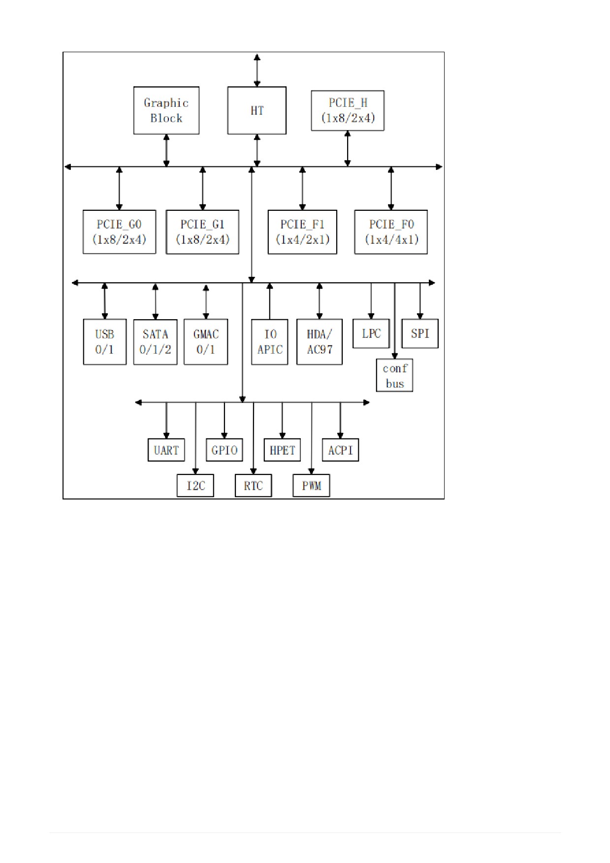
Figure 1. Structure of the Bridge
16
Chapter 2. Bridge and System Clock
2.1. Bridge Clock
The bridge requires a 100Mhz clock and a 32.768 K crystal as reference clock input (and a 33Mhz clock
input if using the LPC bus)
Table 1. Bridge clock
Clock
Frequency
Description
RTC_XO
32.768KHz
32.768KHz Crystal Output
Reserved
TESTCLK
-
LPC_CLKIN
33Mhz
LPC 33Mhz reference clock, unconnected when not
using LPC interface
HTCLKp/n
200Mhz
HT 200Mhz differential reference clock,
unconnected
PCIE_F0_CLKINp/n
100Mhz
PCIE_F0 100Mhz differential reference clock,
unconnected
PCIE_F1_CLKINp/n
100Mhz
PCIE_F1 100Mhz differential reference clock,
unconnected
PCIE_H_CLKINp/n
100Mhz
PCIE_H 100Mhz differential reference clock,
unconnected
PCIE_G0_CLKINp/n
100Mhz
PCIE_G0 100Mhz differential reference clock, can be
left unconnected
PCIE_G1_CLKINp/n
100Mhz
PCIE_G1 100Mhz differential reference clock,
unconnectable
SATA0_CLKINp/n
100Mhz
SATA0 100Mhz differential reference clock, do not
connect
SATA1_CLKINp/n
100Mhz
SATA1 100Mhz differential reference clock, do not
connect
SATA2_CLKINp/n
100Mhz
SATA2 100Mhz differential reference clock, do not
connect
Reserved
USB_XI
12Mhz
12Mhz crystal input
USB_CLKIN
12Mhz
Note: Input clocks not provided need to be grounded through a 10Kohm resistor.
Table 2. Birge clock output
Clock
Frequency
Description
33.3Mhz single-ended clock output. Can be used as
CLKOUT33M
33.3MHz
a memory reference clock for the Loongson 3
processor.
CLKOUT100M
100Mhz
100Mhz single-ended clock output. Can be used as
a reference clock for the HT for the Loongson 3
processor.
17
Clock
Frequency
Description
CLKOUT25M1
25Mhz
25Mhz single-ended clock output. Can be used as a
core reference clock for the Loongson 3 processor.
Variable frequency single-ended clock output.
CLKOUTFLEX1
Variable
Default is 100Mhz.
Note: 1. The CLKO`UT25M and CLKOUTFLEX pins can be multiplexed as GPIO functions.
2.2. Clock-related Configuration Pins
The bridge chip sets a number of pins to set the bridge clock generation method, these configuration pins
are mainly used as a backup design, the normal motherboard design does not need to change the value of
these configuration pins except for CLKSEL[7:6] (dangling or kept as default values). Bridge clock-related
configuration pins are shown in the following table:
Table 3. Bridge chip clock-related configuration pins and descriptions
Pin
Direction
Default
Description
Value
Reserved
SYS_CLKSEL[1:0]
|:
00b
Reserved
SYS_CLKSEL[3:2]
|:
00b
SYS_CLKSEL[5:4]
|:
01b
Reserved
SYS_CLKSEL[6]
|:
0
HT PHY reference clock selection.
0: Use 200MHz differential input clock.
1: Use the 100MHz system input clock.
SYS_CLKSEL[6]
|:
1
HT frequency configuration mode (recommended
setting is 0).
0: The HT clock is configured in software mode. If
the PLL frequency of the HT is not modified using
software, the HT bus frequency remains fixed
(HT1.0 mode: 200MHz; HT3.0 mode: 400MHz).
1: The HT clock can only be used in hardware
configuration mode. In this case, software
modification of the HT PLL frequency is not valid,
and only a few frequencies can be selected via
registers. For HT1.0 mode, 2: 400MHz; 5/9:
800MHz; others: 200MHz;. For HT3.0 mode, 2:
800MHz; 5/9: 1600MHz; others: 400MHz.
Reserved
SYS_CLKSEL[6]
|:
0
2.3. Description of Clock Function
The bridge contains multiple PLLs and clock divider modules to generate the individual clocks needed for
the bridge.
The bridge contains 5 PLLs, each of which can provide up to 3 clock outputs. The five PLLs are used for the
following purposes
18
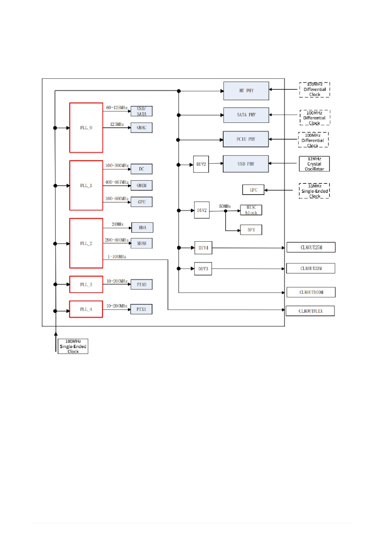
• A device PLL to generate the clocks for USB/SATA, GMAC.
• A graphics PLL to generate clocks for GPU, DC, and graphics memory.
• One system PLL to generate clocks for the internal bus, HDA bitclk, flex clkout.
• Two PIX PLLs for generating two independent pixel clocks to support dual independent displays.
Figure 2. Structure of bridge clock
2.4. Description of PLL Function
The output clock frequency is calculated as follows.
19
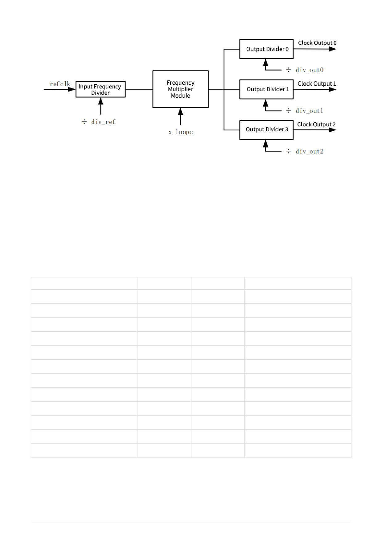
Figure 3. Structure of PLL
clock_out = refclk / div_ref * loopc / divoutN
The refclk of 7A is fixed at 100MHz, and the output of the input divider (refclk
/ div_ref) needs to be
guaranteed to be in the range of 20 In addition, it is necessary to ensure that the output of the input divider
(refclk / div_ref) is in the range of 20 - 40MHz, and the frequency after frequency doubling module
(refclk / div_ref * loopc) is in the range of 1.2GHz - 3.2GHz.
The PLL-related configuration signals and their descriptions are shown in the follow table. The locations of
these configuration signals are shown in Section 4 Bridge Configuration Registers.
Table 4. PLL-related configuration signal description table
Signal
Digit
Direction
Description
pll_div_out0
7
R/W
PLL output clock 0 divisions
pll_div_out1
7
R/W
PLL output clock 1 divisions
R/W
pll_div_out2
7
PLL Output Clock 2 Divisions
R/W
pll_loopc
9
PLL Multiplier
R/W
pll_div_ref
7
PLL Input Divider
RO
pll_locked
1
PLL Lock
sel_pll_out0
1
R/W
Select PLL Output Clock 0
sel_pll_out1
1
R/W
Select PLL Output Clock 1
R/W
sel_pll_out2
1
Select PLL Output Clock 2
R/W
set_pll_param
1
Set PLL configuration parameters
R/W
pll_bypass
1
PLL internal bypass
R/W
pll_pd
1
PLL powerdown
2.5. Configuration Method of PLL
When SYS_CLKSEL[1:0] is 00b, it means the output frequency of PLL can be changed by software. In
this configuration, the default clock frequency at bridge startup is the external reference clock frequency,
20
and software configuration of the bridge clock is required during processor startup. The process of
modifying the clock configuration through software is as follows:
1.
set sel_pll_out* to 0.
2.
set the pll_pd signal to 1.
3.
set set_pll_param to 0.
4.
set the value of pll_div_ref/pll_loopc/pll_div_out*.
5.
set set_pll_param to 1.
6.
set the pll_pd signal to 0.
7.
wait for the PLL lock signal pll_locked to change to 1.
8.
set sel_pll_out* to 1.
21
Chapter 3. Address Space
3.1. Overview of Loongson 3 and Loongson 7A Address
Space
As a bridge for the HT interface, the bridge supports a 40-bit address space internally. Without the
SWIOTLB, the Loongson3 processor + bridge supports a maximum of 1TB of memory address space. To
support multi-processor systems, we use a few bits (up to 4 bits) of the bridge chip’s internal address as
the destination node number for the bridge chip’s internal device DMA access. This means that the bridge
chip can support a processor system with up to 16 nodes. Considering that in practice Loongson uses
systems with up to 4 nodes Therefore, this section describes the maximum number of nodes supported.
For a 4-node system, the address space size for a single processor node is 256GB.
From the CPU’s perspective - that is, the device address space accessible to the CPU - the address space of
a bridge chip consists of three parts: configuration space, PCI I/O space, and PCI MEM space. The address
space of a bridge chip has the same form as the address space defined by PCI.
1. Configuration space: this address space is used to access the configuration headers of the devices
inside the bridge chip (including devices extended through the PCIE bus), and its address composition
conforms to the address organization form of PCI configuration access.
2. I/O space: This address space is used to access the I/O address space defined by the PCI protocol.
Only PCIE has this address space in the bridge chip for accessing downstream devices of the PCIE
controller through I/O type requests.
3. MEM space: All address spaces other than the above two address spaces are MEM spaces.
The bridge chip’s configuration space corresponds to the HT bus configuration space of the HT bus, with a
size of 32MB. the bridge chip’s PCI I/O space corresponds to the HT bus I/O space, with a size of 32MB.
the bridge chip’s PCI MEM space corresponds to the HT bus MEM space, with a size of 1012GB. the PCI
MEM space is used to The PCI MEM space is used to access the MEM space of the bridge’s internal PCIE
devices, the MEM and IO space of devices other than PCIE devices, and the bridge’s configuration register
space.
The latter two address spaces (PCI I/O space and PCI MEM space) are part of the overall processor
address space. and the system software can assign them to any location from 0 - 1TB*. When the software
accesses them, it needs to map them into HT1’s address space segment via the processor’s level 1 XBAR
or directly add HT1’s address space offset to that access address.
Note*: Except for the address segment 0x0f000000-0x0fffffff. This address segment cannot be used
as a bridge device address space.
From the perspective of DMA accesses - that is, accesses to the address space initiated by the bridge
chip’s internal devices - the address space available includes the processor’s memory space and the bridge
chip’s memory space. The size of the processor’s memory space varies depending on the number of nodes
in the system, and the total DMA address space is 1 TB. For a 4-node system, the DMA address space must
be located within the lower 256 GB of the node address space so that the bridge can directly access the
memory of up to 4 nodes. Devices within the bridge chip that can initiate DMA operations include: GPU, DC,
PCIE, USB, SATA, GMAC, HDA, and AC97.
Both types of addresses (the bridge’s address space and the processor’s address space) are addressed in
a uniform manner, i.e., the processor’s memory space, the processor’s configuration space, the bridge’s
configuration access space, the I/O space, and the MEM space, are all located in the same address space
and do not overlap with each other. For a single node system, this address space has a maximum size of
1TB.
The access addresses of the devices inside the bridge chip (PCI I/O space and PCI MEM space) are
designed to be software configurable to support device discovery and management for the PCI
architecture. Each device (device block) inside the bridge contains a PCI configuration header. The
22
software accesses the configuration header to obtain information about the type of the device, the size of
the address space supported, etc., and sets the address space of the device by configuring the device’s
BAR register. This approach is consistent with the 780E.
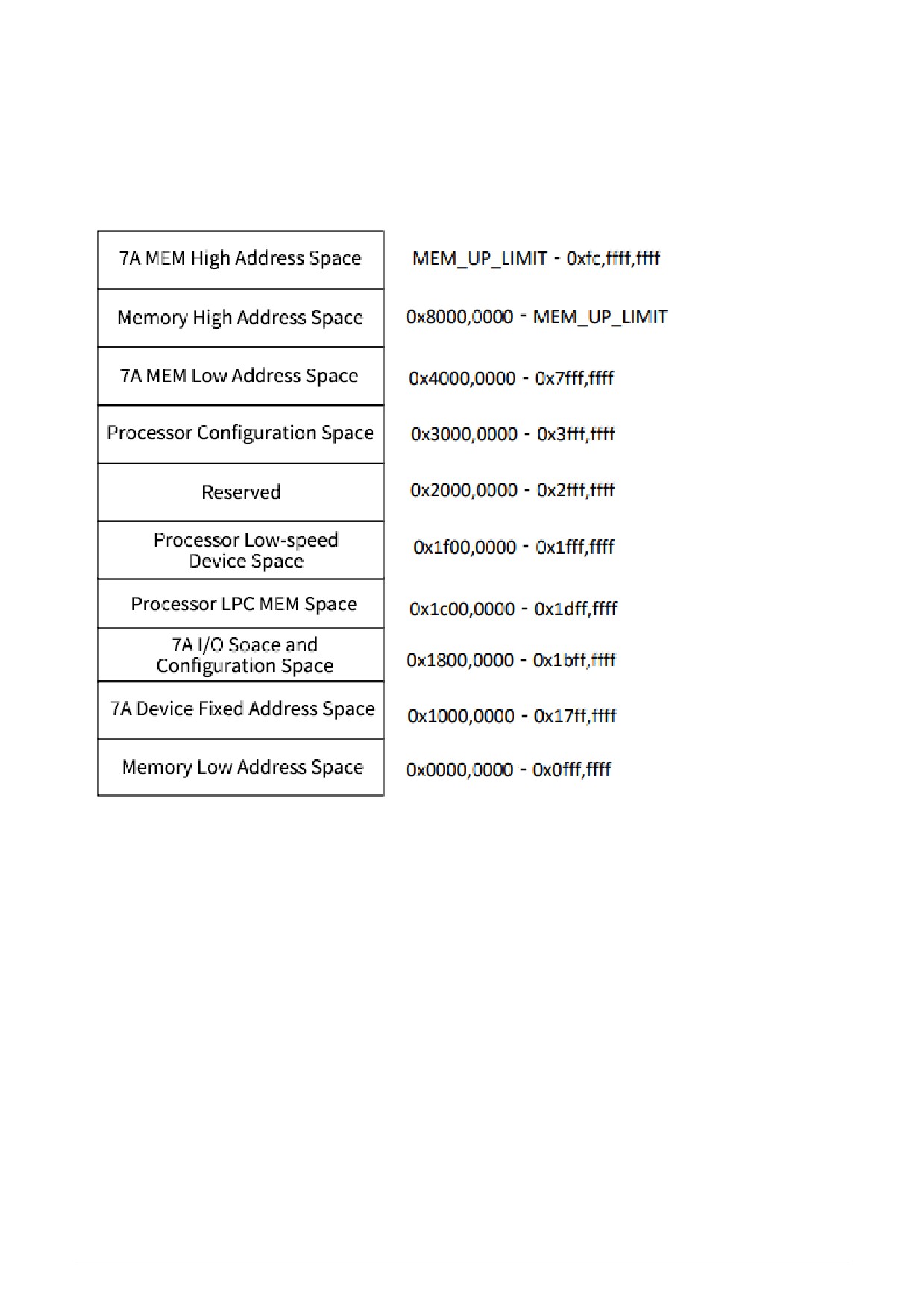
The following is an example of a Loongson 3A+ bridge chip system to illustrate the address space
allocation for the entire computer system. one way of dividing the address space for the 3A+ bridge chip is
shown in the following figure.
Figure 4. Example of address space division for Loongson 3 processor + Loongson 7A bridge
Note: The address in the figure is the low address, not including the node number and high address.
In the address space allocation method in the figure above, the
0x0000,0000 - 0x0fff,ffff is the low 256MB memory space of the system.
0x1000,0000 - 0x17ff,fff is the fixed device address space of the bridge, which includes interrupt
controller, HPET, confbus, MISC low-speed devices, and LPC. ,ffff (HT1’s MEM space)
0x1800,0000 - 0x19ff,ffff is the PCI I/O space of the bridge chip, the software can allocate the I/O
space of the PCIE devices in the bridge chip to this address space, which is mapped to 0xefd,fc00,0000 -
0xefd,fdff through the configuration window of the first-level XBAR, ffff (I/O space of HT1).
0x1a00,0000 - 0x1bff,ffff is the configuration space of the bridge chip, which is used to access the
configuration header of the internal device of the bridge chip, and the access method is compatible with the
PCI protocol, the bit[23:8] of the address bit corresponds to the bus number, device number and func
number in order, and this address is mapped to 0xefd, fe00,0000 - 0xefd,fff,fff (HT1’s bus configuration
space).
23
0x1c00,0000 - 0x1dff,ffff is the LPC MEM address space of 3A.
0x1f00,0000 - 0x1fff,ffff is the 3A’s LPC device space.
0x2000,0000 - 0x2fff,ffff is the reserved space for the processor.
0x3000,0000 - 0x3fff,ffff is the configuration space for 3A.
0x4000,0000 - 0x7fff,ffff is the PCI MEM space of the bridge chip. This address is mapped to
0xe00,4000,0000 - 0xe00,7fff,fff (the MEM space of HT1) through the configuration window of
level 1 XBAR.
0x8000,0000 - MEM_UP_LIMIT is the high memory address space of 3A.
MEM_UP_LIMIT - 0xfc,ffff,ffff is the PCI MEM space of the bridge. This address is mapped to
0xe00,0000,0000+MEM_UP_LIMIT -
0xefc,ffff,ffff (the MEM space of HT1) through the
configuration window of Level 1 XBAR.
3.2. PCI Devices and Functions
Devices with DMA capability inside the bridge and some other devices contain a standard PCI configuration
header. The devices that contain PCI configuration headers include: GPU, DC, PCIE, USB, SATA, GMAC,
HDA/AC97, LPC, and SPI. the bus number, device number, and function number of each device are listed in
the following table
Table 5. Configuration header access correspondence for each device
Bus: Device: Function
Function Description
Bus 0:Device 0:Function 0
HT lo
Bus 0:Device 1:Function 0
HT hi
Bus 0:Device 3:Function 0
GMAC0
Bus 0:Device 3:Function 1
GMAC1
Bus 0:Device 4:Function 0
USB0 OHCI
Bus 0:Device 4:Function 1
USB0 EHCI
Bus 0:Device 5:Function 0
USB1 OHCI
Bus 0:Device 5:Function 1
USB1 EHCI
Bus 0:Device 6:Function 0
GPU
Bus 0:Device 6:Function 1
DC
Bus 0:Device 7:Function 0
HDA1
Bus 0:Device 7:Function 1
AC971
Bus 0:Device 8:Function 0
SATA0
Bus 0:Device 8:Function 1
SATA1
Bus 0:Device 8:Function 2
SATA2
Bus 0:Device 9:Function 0
PCIE_F0 Port02
Bus 0:Device 10:Function 0
PCIE_F0 Port12
Bus 0:Device 11:Function 0
PCIE_F0 Port22
Bus 0:Device 12:Function 0
PCIE_F0 Port32
24
Bus: Device: Function
Function Description
Bus 0:Device 13:Function 0
PCIE_F1 Port03
Bus 0:Device 14:Function 0
PCIE_F1 Port13
Bus 0:Device 15:Function 0
PCIE_G0 port04
Bus 0:Device 16:Function 0
PCIE_G0 port14
Bus 0:Device 17:Function 0
PCIE_G1 port05
Bus 0:Device 18:Function 0
PCIE_G1 port15
Bus 0:Device 19:Function 0
PCIE_H port06
Bus 0:Device 20:Function 0
PCIE_H port16
Bus 0:Device 22:Function 0
SPI
Bus 0:Device 23:Function 0
LPC7
Notes.
1. when hda_sel is 1, HDA controller can be discovered; when hda_sel is 0, AC97 controller can be
discovered.
2. When PCIE_F0 works in x4 mode, only Port 0 is visible, Port 1-3 is not visible; when PCIE_F0 works in
non-x4 mode, Port 0-3 is visible. When PCIE_F0 works in non-x4 mode, Port 0-3 is visible. 3.
3. When PCIE_F1 is operating in x4 mode, only Port 0 is visible and Port 1 is not visible; when PCIE_F1 is
operating in non-x4 mode, Port 0-1 is visible. When PCIE_F1 is operating in non-x4 mode, Port 0-1 is
visible. 4.
4. When PCIE_G0 is operating in x8 mode, only Port 0 is visible and Port 1 is not visible; when PCIE_G0 is
operating in x4 mode, Port 0-1 is visible. mode, Port 0-1 is visible. 5.
5. When PCIE_G1 is operating in x8 mode, only Port 0 is visible and Port 1 is not visible; when PCIE_G1 is
operating in x4 mode, Port 0-1 is visible. When PCIE_G1 is operating in x4 mode, Port 0-1 is visible. 6.
6. When PCIE_H is operating in x8 mode, only Port 0 is visible and Port 1 is not visible; when PCIE_H is
operating in x4 mode, Port 0-1 is visible.
7. LPC(D23:F0) is only visible when LPC module is enabled.
When the bus number, device number, function number and address offset accessed by the configuration
header are invalid, the write operation is invalid; the data obtained by the read operation is 0xFFFFFFFF.
3.3. Access Address of the PCI Configuration
The processor can access the configuration space of the bridge chip through two address spaces. One is
the standard configuration access space defined by HT (0xFD_FE00_0000 - 0xFD_FFFF_FFFF) and the
other is the reserved address space of HT (0xFE_0000_0000 - 0xFE_1FFF_FFFF). The configuration space
size for each bridge device accessed through the HT standard configuration access space is 256 bytes; the
configuration space size for each bridge device accessed through the reserved address space is 4K bytes.
The maximum configuration space size per device is 256 bytes when using the HT-defined standard
configuration access space (0xFD_FE00_0000-0xFD_FFFF_FFFF) to access the bridge slice. The address
[39:24] determines the configuration header type (0xFDFE is Type0, 0xFDFF is Type1); [23:16] indicates the
Bus Number; [15:11] indicates the Device Number; [10:8] indicates the Function Number; [7:0] indicates the
offset. The following diagram shows the meaning of the address segment for the CPU to access the PCI
configuration space using the HT standard configuration access space
25
///////////////////////////////////////