Intel 64 and IA-32 Architectures. Software Developer’s Manual (Collection, 2023) - page 117

VMX INSTRUCTION REFERENCE
31.4
VM INSTRUCTION ERROR NUMBERS
For certain error conditions, the VM-instruction error field is loaded with an error number to indicate the source of
the error. Table 31-1 lists VM-instruction error numbers.
Table 31-1. VM-Instruction Error Numbers
Error
Description
Number
1
VMCALL executed in VMX root operation
2
VMCLEAR with invalid physical address
3
VMCLEAR with VMXON pointer
4
VMLAUNCH with non-clear VMCS
5
VMRESUME with non-launched VMCS
6
VMRESUME after VMXOFF (VMXOFF and VMXON between VMLAUNCH and VMRESUME)a
7
VM entry with invalid control field(s)b,c
8
VM entry with invalid host-state field(s)b
9
VMPTRLD with invalid physical address
10
VMPTRLD with VMXON pointer
11
VMPTRLD with incorrect VMCS revision identifier
12
VMREAD/VMWRITE from/to unsupported VMCS component
13
VMWRITE to read-only VMCS component
15
VMXON executed in VMX root operation
16
VM entry with invalid executive-VMCS pointerb
17
VM entry with non-launched executive VMCSb
18
VM entry with executive-VMCS pointer not VMXON pointer (when attempting to deactivate the dual-monitor treatment of
SMIs and SMM)b
19
VMCALL with non-clear VMCS (when attempting to activate the dual-monitor treatment of SMIs and SMM)
20
VMCALL with invalid VM-exit control fields
22
VMCALL with incorrect MSEG revision identifier (when attempting to activate the dual-monitor treatment of SMIs and SMM)
23
VMXOFF under dual-monitor treatment of SMIs and SMM
24
VMCALL with invalid SMM-monitor features (when attempting to activate the dual-monitor treatment of SMIs and SMM)
25
VM entry with invalid VM-execution control fields in executive VMCS (when attempting to return from SMM)b,c
26
VM entry with events blocked by MOV SS.
28
Invalid operand to INVEPT/INVVPID.
NOTES:
a. Earlier versions of this manual described this error as “VMRESUME with a corrupted VMCS”.
b. VM-entry checks on control fields and host-state fields may be performed in any order. Thus, an indication by error number of one
cause does not imply that there are not also other errors. Different processors may give different error numbers for the same VMCS.
c. Error number 7 is not used for VM entries that return from SMM that fail due to invalid VM-execution control fields in the executive
VMCS. Error number 25 is used for these cases.
Vol. 3C
31-31
VMX INSTRUCTION REFERENCE
31-32
Vol. 3C

CHAPTER 32
SYSTEM MANAGEMENT MODE
This chapter describes aspects of IA-64 and IA-32 architecture used in system management mode (SMM).
SMM provides an alternate operating environment that can be used to monitor and manage various system
resources for more efficient energy usage, to control system hardware, and/or to run proprietary code. It was
introduced into the IA-32 architecture in the Intel386 SL processor (a mobile specialized version of the Intel386
processor). It is also available in the Pentium M, Pentium 4, Intel Xeon, P6 family, and Pentium and Intel486
processors (beginning with the enhanced versions of the Intel486 SL and Intel486 processors).
32.1
SYSTEM MANAGEMENT MODE OVERVIEW
SMM is a special-purpose operating mode provided for handling system-wide functions like power management,
system hardware control, or proprietary OEM-designed code. It is intended for use only by system firmware, not by
applications software or general-purpose systems software. The main benefit of SMM is that it offers a distinct and
easily isolated processor environment that operates transparently to the operating system or executive and soft-
ware applications.
When SMM is invoked through a system management interrupt (SMI), the processor saves the current state of the
processor (the processor’s context), then switches to a separate operating environment defined by a new address
space. The system management software executive (SMI handler) starts execution in that environment, and the
critical code and data of the SMI handler reside in a physical memory region (SMRAM) within that address space.
While in SMM, the processor executes SMI handler code to perform operations such as powering down unused disk
drives or monitors, executing proprietary code, or placing the whole system in a suspended state. When the SMI
handler has completed its operations, it executes a resume (RSM) instruction. This instruction causes the processor
to reload the saved context of the processor, switch back to protected or real mode, and resume executing the
interrupted application or operating-system program or task.
The following SMM mechanisms make it transparent to applications programs and operating systems:
• The only way to enter SMM is by means of an SMI.
• The processor executes SMM code in a separate address space that can be made inaccessible from the other
operating modes.
• Upon entering SMM, the processor saves the context of the interrupted program or task.
• All interrupts normally handled by the operating system are disabled upon entry into SMM.
• The RSM instruction can be executed only in SMM.
Section 32.3 describes transitions into and out of SMM. The execution environment after entering SMM is in real-
address mode with paging disabled (CR0.PE = CR0.PG = 0). In this initial execution environment, the SMI handler
can address up to 4 GBytes of memory and can execute all I/O and system instructions. Section 32.5 describes in
detail the initial SMM execution environment for an SMI handler and operation within that environment. The SMI
handler may subsequently switch to other operating modes while remaining in SMM.
NOTES
Software developers should be aware that, even if a logical processor was using the physical-
address extension (PAE) mechanism (introduced in the P6 family processors) or was in IA-32e
mode before an SMI, this will not be the case after the SMI is delivered. This is because delivery of
an SMI disables paging (see Table 32-4). (This does not apply if the dual-monitor treatment of SMIs
and SMM is active; see Section 32.15.)
Vol. 3C
32-1

SYSTEM MANAGEMENT MODE
32.1.1 System Management Mode and VMX Operation
Traditionally, SMM services system management interrupts and then resumes program execution (back to the soft-
ware stack consisting of executive and application software; see Section 32.2 through Section 32.13).
A virtual machine monitor (VMM) using VMX can act as a host to multiple virtual machines and each virtual machine
can support its own software stack of executive and application software. On processors that support VMX, virtual-
machine extensions may use system-management interrupts (SMIs) and system-management mode (SMM) in one
of two ways:
• Default treatment. System firmware handles SMIs. The processor saves architectural states and critical
states relevant to VMX operation upon entering SMM. When the firmware completes servicing SMIs, it uses
RSM to resume VMX operation.
• Dual-monitor treatment. Two VM monitors collaborate to control the servicing of SMIs: one VMM operates
outside of SMM to provide basic virtualization in support for guests; the other VMM operates inside SMM (while
in VMX operation) to support system-management functions. The former is referred to as executive monitor,
the latter SMM-transfer monitor (STM).1
The default treatment is described in Section 32.14, “Default Treatment of SMIs and SMM with VMX Operation and
SMX Operation.” Dual-monitor treatment of SMM is described in Section 32.15, “Dual-Monitor Treatment of SMIs
and SMM.”
32.2
SYSTEM MANAGEMENT INTERRUPT (SMI)
The only way to enter SMM is by signaling an SMI through the SMI# pin on the processor or through an SMI
message received through the APIC bus. The SMI is a nonmaskable external interrupt that operates independently
from the processor’s interrupt- and exception-handling mechanism and the local APIC. The SMI takes precedence
over an NMI and a maskable interrupt. SMM is non-reentrant; that is, the SMI is disabled while the processor is in
SMM.
NOTES
In the Pentium 4, Intel Xeon, and P6 family processors, when a processor that is designated as an
application processor during an MP initialization sequence is waiting for a startup IPI (SIPI), it is in
a mode where SMIs are masked. However if a SMI is received while an application processor is in
the wait for SIPI mode, the SMI will be pended. The processor then responds on receipt of a SIPI by
immediately servicing the pended SMI and going into SMM before handling the SIPI.
An SMI may be blocked for one instruction following execution of STI, MOV to SS, or POP into SS.
32.3
SWITCHING BETWEEN SMM AND THE OTHER PROCESSOR OPERATING
MODES
Figure 2-3 shows how the processor moves between SMM and the other processor operating modes (protected,
real-address, and virtual-8086). Signaling an SMI while the processor is in real-address, protected, or virtual-8086
modes always causes the processor to switch to SMM. Upon execution of the RSM instruction, the processor always
returns to the mode it was in when the SMI occurred.
32.3.1 Entering SMM
The processor always handles an SMI on an architecturally defined “interruptible” point in program execution
(which is commonly at an IA-32 architecture instruction boundary). When the processor receives an SMI, it waits
for all instructions to retire and for all stores to complete. The processor then saves its current context in SMRAM
(see Section 32.4), enters SMM, and begins to execute the SMI handler.
1. The dual-monitor treatment may not be supported by all processors. Software should consult the VMX capability MSR IA32_VMX-
_BASIC (see Appendix A.1) to determine whether it is supported.
32-2
Vol. 3C
SYSTEM MANAGEMENT MODE
Upon entering SMM, the processor signals external hardware that SMI handling has begun. The signaling mecha-
nism used is implementation dependent. For the P6 family processors, an SMI acknowledge transaction is gener-
ated on the system bus and the multiplexed status signal EXF4 is asserted each time a bus transaction is generated
while the processor is in SMM. For the Pentium and Intel486 processors, the SMIACT# pin is asserted.
An SMI has a greater priority than debug exceptions and external interrupts. Thus, if an NMI, maskable hardware
interrupt, or a debug exception occurs at an instruction boundary along with an SMI, only the SMI is handled.
Subsequent SMI requests are not acknowledged while the processor is in SMM. The first SMI interrupt request that
occurs while the processor is in SMM (that is, after SMM has been acknowledged to external hardware) is latched
and serviced when the processor exits SMM with the RSM instruction. The processor will latch only one SMI while
in SMM.
See Section 32.5 for a detailed description of the execution environment when in SMM.
32.3.2 Exiting From SMM
The only way to exit SMM is to execute the RSM instruction. The RSM instruction is only available to the SMI
handler; if the processor is not in SMM, attempts to execute the RSM instruction result in an invalid-opcode excep-
tion (#UD) being generated.
The RSM instruction restores the processor’s context by loading the state save image from SMRAM back into the
processor’s registers. The processor then returns an SMIACK transaction on the system bus and returns program
control back to the interrupted program.
NOTE
On processors that support the shadow-stack feature, RSM loads the SSP register from the state
save image in SMRAM (see Table 32-3). The value is made canonical by sign-extension before
loading it into SSP.
Upon successful completion of the RSM instruction, the processor signals external hardware that SMM has been
exited. For the P6 family processors, an SMI acknowledge transaction is generated on the system bus and the
multiplexed status signal EXF4 is no longer generated on bus cycles. For the Pentium and Intel486 processors, the
SMIACT# pin is deserted.
If the processor detects invalid state information saved in the SMRAM, it enters the shutdown state and generates
a special bus cycle to indicate it has entered shutdown state. Shutdown happens only in the following situations:
• A reserved bit in control register CR4 is set to 1 on a write to CR4. This error should not happen unless SMI
handler code modifies reserved areas of the SMRAM saved state map (see Section 32.4.1). CR4 is saved in the
state map in a reserved location and cannot be read or modified in its saved state.
• An illegal combination of bits is written to control register CR0, in particular PG set to 1 and PE set to 0, or NW
set to 1 and CD set to 0.
• CR4.PCIDE would be set to 1 and IA32_EFER.LMA to 0.
•
(For the Pentium and Intel486 processors only.) If the address stored in the SMBASE register when an RSM
instruction is executed is not aligned on a 32-KByte boundary. This restriction does not apply to the P6 family
processors.
• CR4.CET would be set to 1 and CR0.WP to 0.
In the shutdown state, Intel processors stop executing instructions until a RESET#, INIT# or NMI# is asserted.
While Pentium family processors recognize the SMI# signal in shutdown state, P6 family and Intel486 processors
do not. Intel does not support using SMI# to recover from shutdown states for any processor family; the response
of processors in this circumstance is not well defined. On Pentium 4 and later processors, shutdown will inhibit INTR
and A20M but will not change any of the other inhibits. On these processors, NMIs will be inhibited if no action is
taken in the SMI handler to uninhibit them (see Section 32.8).
If the processor is in the HALT state when the SMI is received, the processor handles the return from SMM slightly
differently (see Section 32.10). Also, the SMBASE address can be changed on a return from SMM (see Section
32.11).
Vol. 3C
32-3

SYSTEM MANAGEMENT MODE
32.4
SMRAM
Upon entering SMM, the processor switches to a new address space. Because paging is disabled upon entering
SMM, this initial address space maps all memory accesses to the low 4 GBytes of the processor's physical address
space. The SMI handler's critical code and data reside in a memory region referred to as system-management RAM
(SMRAM). The processor uses a pre-defined region within SMRAM to save the processor's pre-SMI context. SMRAM
can also be used to store system management information (such as the system configuration and specific informa-
tion about powered-down devices) and OEM-specific information.
The default SMRAM size is 64 KBytes beginning at a base physical address in physical memory called the SMBASE
(see Figure 32-1). The SMBASE default value following a hardware reset is 30000H. The processor looks for the
first instruction of the SMI handler at the address [SMBASE + 8000H]. It stores the processor’s state in the area
from [SMBASE + FE00H] to [SMBASE + FFFFH]. See Section 32.4.1 for a description of the mapping of the state
save area.
The system logic is minimally required to decode the physical address range for the SMRAM from [SMBASE +
8000H] to [SMBASE + FFFFH]. A larger area can be decoded if needed. The size of this SMRAM can be between 32
KBytes and 4 GBytes.
The location of the SMRAM can be changed by changing the SMBASE value (see Section 32.11). It should be noted
that all processors in a multiple-processor system are initialized with the same SMBASE value (30000H). Initializa-
tion software must sequentially place each processor in SMM and change its SMBASE so that it does not overlap
those of other processors.
The actual physical location of the SMRAM can be in system memory or in a separate RAM memory. The processor
generates an SMI acknowledge transaction (P6 family processors) or asserts the SMIACT# pin (Pentium and
Intel486 processors) when the processor receives an SMI (see Section 32.3.1).
System logic can use the SMI acknowledge transaction or the assertion of the SMIACT# pin to decode accesses to
the SMRAM and redirect them (if desired) to specific SMRAM memory. If a separate RAM memory is used for
SMRAM, system logic should provide a programmable method of mapping the SMRAM into system memory space
when the processor is not in SMM. This mechanism will enable start-up procedures to initialize the SMRAM space
(that is, load the SMI handler) before executing the SMI handler during SMM.
32.4.1 SMRAM State Save Map
When an IA-32 processor that does not support Intel 64 architecture initially enters SMM, it writes its state to the
state save area of the SMRAM. The state save area begins at [SMBASE + 8000H + 7FFFH] and extends down to
[SMBASE + 8000H + 7E00H]. Table 32-1 shows the state save map. The offset in column 1 is relative to the
SMBASE value plus 8000H. Reserved spaces should not be used by software.
Some of the registers in the SMRAM state save area (marked YES in column 3) may be read and changed by the
SMI handler, with the changed values restored to the processor registers by the RSM instruction. Some register
images are read-only, and must not be modified (modifying these registers will result in unpredictable behavior).
An SMI handler should not rely on any values stored in an area that is marked as reserved.
SMRAM
SMBASE + FFFFH
Start of State Save Area
SMI Handler Entry Point
SMBASE + 8000H
SMBASE
Figure 32-1. SMRAM Usage
32-4
Vol. 3C

SYSTEM MANAGEMENT MODE
Table 32-1. SMRAM State Save Map
Offset
Register
Writable?
(Added to SMBASE + 8000H)
7FFCH
CR0
No
7FF8H
CR3
No
7FF4H
EFLAGS
Yes
7FF0H
EIP
Yes
7FECH
EDI
Yes
7FE8H
ESI
Yes
7FE4H
EBP
Yes
7FE0H
ESP
Yes
7FDCH
EBX
Yes
7FD8H
EDX
Yes
7FD4H
ECX
Yes
7FD0H
EAX
Yes
7FCCH
DR6
No
7FC8H
DR7
No
7FC4H
TR1
No
7FC0H
Reserved
No
7FBCH
GS1
No
7FB8H
FS1
No
7FB4H
DS1
No
7FB0H
SS1
No
7FACH
CS1
No
7FA8H
ES1
No
7FA4H
I/O State Field, see Section 32.7
No
7FA0H
I/O Memory Address Field, see Section 32.7
No
7F9FH-7F03H
Reserved
No
7F02H
Auto HALT Restart Field (Word)
Yes
7F00H
I/O Instruction Restart Field (Word)
Yes
7EFCH
SMM Revision Identifier Field (Doubleword)
No
7EF8H
SMBASE Field (Doubleword)
Yes
7EF7H - 7E00H
Reserved
No
NOTE:
1. The two most significant bytes are reserved.
The following registers are saved (but not readable) and restored upon exiting SMM:
• Control register CR4. (This register is cleared to all 0s when entering SMM).
• The hidden segment descriptor information stored in segment registers CS, DS, ES, FS, GS, and SS.
If an SMI request is issued for the purpose of powering down the processor, the values of all reserved locations in
the SMM state save must be saved to nonvolatile memory.
The following state is not automatically saved and restored following an SMI and the RSM instruction, respectively:
Vol. 3C
32-5

SYSTEM MANAGEMENT MODE
• Debug registers DR0 through DR3.
• The x87 FPU registers.
• The MTRRs.
• Control register CR2.
• The model-specific registers (for the P6 family and Pentium processors) or test registers TR3 through TR7 (for
the Pentium and Intel486 processors).
• The state of the trap controller.
• The machine-check architecture registers.
• The APIC internal interrupt state (ISR, IRR, etc.).
• The microcode update state.
If an SMI is used to power down the processor, a power-on reset will be required before returning to SMM, which
will reset much of this state back to its default values. So an SMI handler that is going to trigger power down should
first read these registers listed above directly, and save them (along with the rest of RAM) to nonvolatile storage.
After the power-on reset, the continuation of the SMI handler should restore these values, along with the rest of
the system's state. Anytime the SMI handler changes these registers in the processor, it must also save and restore
them.
NOTES
A small subset of the MSRs (such as, the time-stamp counter and performance-monitoring
counters) are not arbitrarily writable and therefore cannot be saved and restored. SMM-based
power-down and restoration should only be performed with operating systems that do not use or
rely on the values of these registers.
Operating system developers should be aware of this fact and ensure that their operating-system
assisted power-down and restoration software is immune to unexpected changes in these register
values.
32.4.1.1 SMRAM State Save Map and Intel 64 Architecture
When the processor initially enters SMM, it writes its state to the state save area of the SMRAM. The state save area
on an Intel 64 processor at [SMBASE + 8000H + 7FFFH] and extends to [SMBASE + 8000H + 7C00H].
Support for Intel 64 architecture is reported by CPUID.80000001:EDX[29] = 1. The layout of the SMRAM state save
map is shown in Table 32-3.
Additionally, the SMRAM state save map shown in Table 32-3 also applies to processors with the following CPUID
signatures listed in Table 32-2, irrespective of the value in CPUID.80000001:EDX[29].
Table 32-2. Processor Signatures and 64-bit SMRAM State Save Map Format
DisplayFamily_DisplayModel
Processor Families/Processor Number Series
06_17H
Intel Xeon Processor 5200, 5400 series, Intel Core 2 Quad processor Q9xxx, Intel Core 2 Duo
processors E8000, T9000,
06_0FH
Intel Xeon Processor 3000, 3200, 5100, 5300, 7300 series, Intel Core 2 Quad, Intel Core 2 Extreme,
Intel Core 2 Duo processors, Intel Pentium dual-core processors
06_1CH
45 nm Intel Atom® processors
32-6
Vol. 3C

SYSTEM MANAGEMENT MODE
Table 32-3. SMRAM State Save Map for Intel 64 Architecture
Offset
Register
Writable?
(Added to SMBASE + 8000H)
7FF8H
CR0
No
7FF0H
CR3
No
7FE8H
RFLAGS
Yes
7FE0H
IA32_EFER
Yes
7FD8H
RIP
Yes
7FD0H
DR6
No
7FC8H
DR7
No
7FC4H
TR SEL1
No
7FC0H
LDTR SEL1
No
7FBCH
GS SEL1
No
7FB8H
FS SEL1
No
7FB4H
DS SEL1
No
7FB0H
SS SEL1
No
7FACH
CS SEL1
No
7FA8H
ES SEL1
No
7FA4H
IO_MISC
No
7F9CH
IO_MEM_ADDR
No
7F94H
RDI
Yes
7F8CH
RSI
Yes
7F84H
RBP
Yes
7F7CH
RSP
Yes
7F74H
RBX
Yes
7F6CH
RDX
Yes
7F64H
RCX
Yes
7F5CH
RAX
Yes
7F54H
R8
Yes
7F4CH
R9
Yes
7F44H
R10
Yes
7F3CH
R11
Yes
7F34H
R12
Yes
7F2CH
R13
Yes
7F24H
R14
Yes
7F1CH
R15
Yes
7F1BH-7F04H
Reserved
No
7F02H
Auto HALT Restart Field (Word)
Yes
7F00H
I/O Instruction Restart Field (Word)
Yes
7EFCH
SMM Revision Identifier Field (Doubleword)
No
7EF8H
SMBASE Field (Doubleword)
Yes
Vol. 3C
32-7

SYSTEM MANAGEMENT MODE
Table 32-3. SMRAM State Save Map for Intel 64 Architecture (Contd.)
Offset
Register
Writable?
(Added to SMBASE + 8000H)
7EF7H - 7EE4H
Reserved
No
7EE0H
Setting of “enable EPT” VM-execution control
No
7ED8H
Value of EPTP VM-execution control field
No
7ED7H - 7ECC0H
Reserved
No
7EC8H
SSP
Yes
7EC7H - 7EA0H
Reserved
No
7E9CH
LDT Base (lower 32 bits)
No
7E98H
Reserved
No
7E94H
IDT Base (lower 32 bits)
No
7E90H
Reserved
No
7E8CH
GDT Base (lower 32 bits)
No
7E8BH - 7E48H
Reserved
No
7E40H
CR4 (64 bits)
No
7E3FH - 7DF0H
Reserved
No
7DE8H
IO_RIP
Yes
7DE7H - 7DDCH
Reserved
No
7DD8H
IDT Base (Upper 32 bits)
No
7DD4H
LDT Base (Upper 32 bits)
No
7DD0H
GDT Base (Upper 32 bits)
No
7DCFH - 7C00H
Reserved
No
NOTE:
1. The two most significant bytes are reserved.
32.4.2 SMRAM Caching
An IA-32 processor does not automatically write back and invalidate its caches before entering SMM or before
exiting SMM. Because of this behavior, care must be taken in the placement of the SMRAM in system memory and
in the caching of the SMRAM to prevent cache incoherence when switching back and forth between SMM and
protected mode operation. Any of the following three methods of locating the SMRAM in system memory will guar-
antee cache coherency.
• Place the SMRAM in a dedicated section of system memory that the operating system and applications are
prevented from accessing. Here, the SMRAM can be designated as cacheable (WB, WT, or WC) for optimum
processor performance, without risking cache incoherence when entering or exiting SMM.
• Place the SMRAM in a section of memory that overlaps an area used by the operating system (such as the video
memory), but designate the SMRAM as uncacheable (UC). This method prevents cache access when in SMM to
maintain cache coherency, but the use of uncacheable memory reduces the performance of SMM code.
• Place the SMRAM in a section of system memory that overlaps an area used by the operating system and/or
application code, but explicitly flush (write back and invalidate) the caches upon entering and exiting SMM
mode. This method maintains cache coherency, but incurs the overhead of two complete cache flushes.
For Pentium 4, Intel Xeon, and P6 family processors, a combination of the first two methods of locating the SMRAM
is recommended. Here the SMRAM is split between an overlapping and a dedicated region of memory. Upon
entering SMM, the SMRAM space that is accessed overlaps video memory (typically located in low memory). This
SMRAM section is designated as UC memory. The initial SMM code then jumps to a second SMRAM section that is
32-8
Vol. 3C

SYSTEM MANAGEMENT MODE
located in a dedicated region of system memory (typically in high memory). This SMRAM section can be cached for
optimum processor performance.
For systems that explicitly flush the caches upon entering SMM (the third method described above), the cache flush
can be accomplished by asserting the FLUSH# pin at the same time as the request to enter SMM (generally initi-
ated by asserting the SMI# pin). The priorities of the FLUSH# and SMI# pins are such that the FLUSH# is serviced
first. To guarantee this behavior, the processor requires that the following constraints on the interaction of FLUSH#
and SMI# be met. In a system where the FLUSH# and SMI# pins are synchronous and the set up and hold times
are met, then the FLUSH# and SMI# pins may be asserted in the same clock. In asynchronous systems, the
FLUSH# pin must be asserted at least one clock before the SMI# pin to guarantee that the FLUSH# pin is serviced
first.
Upon leaving SMM (for systems that explicitly flush the caches), the WBINVD instruction should be executed prior
to leaving SMM to flush the caches.
NOTES
In systems based on the Pentium processor that use the FLUSH# pin to write back and invalidate
cache contents before entering SMM, the processor will prefetch at least one cache line in between
when the Flush Acknowledge cycle is run and the subsequent recognition of SMI# and the assertion
of SMIACT#.
It is the obligation of the system to ensure that these lines are not cached by returning KEN#
inactive to the Pentium processor.
32.4.2.1 System Management Range Registers (SMRR)
SMI handler code and data stored by SMM code resides in SMRAM. The SMRR interface is an enhancement in Intel
64 architecture to limit cacheable reference of addresses in SMRAM to code running in SMM. The SMRR interface
can be configured only by code running in SMM. Details of SMRR is described in Section 12.11.2.4.
32.5
SMI HANDLER EXECUTION ENVIRONMENT
Section 32.5.1 describes the initial execution environment for an SMI handler. An SMI handler may re-configure its
execution environment to other supported operating modes. Section 32.5.2 discusses modifications an SMI
handler can make to its execution environment. Section 32.5.3 discusses Control-flow Enforcement Technology
(CET) interactions in the environment.
32.5.1 Initial SMM Execution Environment
After saving the current context of the processor, the processor initializes its core registers to the values shown in
Table 32-4. Upon entering SMM, the PE and PG flags in control register CR0 are cleared, which places the processor
in an environment similar to real-address mode. The differences between the SMM execution environment and the
real-address mode execution environment are as follows:
• The addressable address space ranges from 0 to FFFFFFFFH (4 GBytes).
• The normal 64-KByte segment limit for real-address mode is increased to 4 GBytes.
• The default operand and address sizes are set to 16 bits, which restricts the addressable SMRAM address space
to the 1-MByte real-address mode limit for native real-address-mode code. However, operand-size and
address-size override prefixes can be used to access the address space beyond the 1-MByte.
Table 32-4. Processor Register Initialization in SMM
Register
Contents
General-purpose registers
Undefined
EFLAGS
00000002H
EIP
00008000H
CS selector
SMM Base shifted right 4 bits (default 3000H)
Vol. 3C
32-9

SYSTEM MANAGEMENT MODE
Table 32-4. Processor Register Initialization in SMM
CS base
SMM Base (default 30000H)
DS, ES, FS, GS, SS Selectors
0000H
DS, ES, FS, GS, SS Bases
000000000H
DS, ES, FS, GS, SS Limits
0FFFFFFFFH
CR0
PE, EM, TS, and PG flags set to 0; others unmodified
CR4
Cleared to zero
DR6
Undefined
DR7
00000400H
• Near jumps and calls can be made to anywhere in the 4-GByte address space if a 32-bit operand-size override
prefix is used. Due to the real-address-mode style of base-address formation, a far call or jump cannot transfer
control to a segment with a base address of more than 20 bits (1 MByte). However, since the segment limit in
SMM is 4 GBytes, offsets into a segment that go beyond the 1-MByte limit are allowed when using 32-bit
operand-size override prefixes. Any program control transfer that does not have a 32-bit operand-size override
prefix truncates the EIP value to the 16 low-order bits.
• Data and the stack can be located anywhere in the 4-GByte address space, but can be accessed only with a 32-
bit address-size override if they are located above 1 MByte. As with the code segment, the base address for a
data or stack segment cannot be more than 20 bits.
The value in segment register CS is automatically set to the default of 30000H for the SMBASE shifted 4 bits to the
right; that is, 3000H. The EIP register is set to 8000H. When the EIP value is added to shifted CS value (the
SMBASE), the resulting linear address points to the first instruction of the SMI handler.
The other segment registers (DS, SS, ES, FS, and GS) are cleared to 0 and their segment limits are set to 4 GBytes.
In this state, the SMRAM address space may be treated as a single flat 4-GByte linear address space. If a segment
register is loaded with a 16-bit value, that value is then shifted left by 4 bits and loaded into the segment base
(hidden part of the segment register). The limits and attributes are not modified.
Maskable hardware interrupts, exceptions, NMI interrupts, SMI interrupts, A20M interrupts, single-step traps,
breakpoint traps, and INIT operations are inhibited when the processor enters SMM. Maskable hardware interrupts,
exceptions, single-step traps, and breakpoint traps can be enabled in SMM if the SMM execution environment
provides and initializes an interrupt table and the necessary interrupt and exception handlers (see Section 32.6).
32.5.2 SMI Handler Operating Mode Switching
Within SMM, an SMI handler may change the processor's operating mode (e.g., to enable PAE paging, enter 64-bit
mode, etc.) after it has made proper preparation and initialization to do so. For example, if switching to 32-bit
protected mode, the SMI handler should follow the guidelines provided in Chapter 10, “Processor Management and
Initialization.” If the SMI handler does wish to change operating mode, it is responsible for executing the appro-
priate mode-transition code after each SMI.
It is recommended that the SMI handler make use of all means available to protect the integrity of its critical code
and data. In particular, it should use the system-management range register (SMRR) interface if it is available (see
Section 11.11.2.4). The SMRR interface can protect only the first 4 GBytes of the physical address space. The SMI
handler should take that fact into account if it uses operating modes that allow access to physical addresses beyond
that 4-GByte limit (e.g., PAE paging or 64-bit mode).
Execution of the RSM instruction restores the pre-SMI processor state from the SMRAM state-state map (see
Section 32.4.1) into which it was stored when the processor entered SMM. (The SMBASE field in the SMRAM state-
save map does not determine the state following RSM but rather the initial environment following the next entry to
SMM.) Any required change to operating mode is performed by the RSM instruction; there is no need for the SMI
handler to change modes explicitly prior to executing RSM.
32-10
Vol. 3C
SYSTEM MANAGEMENT MODE
32.5.3 Control-flow Enforcement Technology Interactions
On processors that support CET shadow stacks, when the processor enters SMM, the processor saves the SSP
register to the SMRAM state save area (see Table 32-3) and clears CR4.CET to 0. Thus, the initial execution envi-
ronment of the SMI handler has CET disabled and all of the CET state of the interrupted program is still in the
machine. An SMM that uses CET is required to save the interrupted program’s CET state and restore the CET state
prior to exiting SMM.
32.6
EXCEPTIONS AND INTERRUPTS WITHIN SMM
When the processor enters SMM, all hardware interrupts are disabled in the following manner:
• The IF flag in the EFLAGS register is cleared, which inhibits maskable hardware interrupts from being
generated.
• The TF flag in the EFLAGS register is cleared, which disables single-step traps.
• Debug register DR7 is cleared, which disables breakpoint traps. (This action prevents a debugger from acciden-
tally breaking into an SMI handler if a debug breakpoint is set in normal address space that overlays code or
data in SMRAM.)
• NMI, SMI, and A20M interrupts are blocked by internal SMM logic. (See Section 32.8 for more information
about how NMIs are handled in SMM.)
Software-invoked interrupts and exceptions can still occur, and maskable hardware interrupts can be enabled by
setting the IF flag. Intel recommends that SMM code be written in so that it does not invoke software interrupts
(with the INT n, INTO, INT1, INT3, or BOUND instructions) or generate exceptions.
If the SMI handler requires interrupt and exception handling, an SMM interrupt table and the necessary exception
and interrupt handlers must be created and initialized from within SMM. Until the interrupt table is correctly initial-
ized (using the LIDT instruction), exceptions and software interrupts will result in unpredictable processor
behavior.
The following restrictions apply when designing SMM interrupt and exception-handling facilities:
• The interrupt table should be located at linear address 0 and must contain real-address mode style interrupt
vectors (4 bytes containing CS and IP).
• Due to the real-address mode style of base address formation, an interrupt or exception cannot transfer control
to a segment with a base address of more that 20 bits.
• An interrupt or exception cannot transfer control to a segment offset of more than 16 bits (64 KBytes).
• When an exception or interrupt occurs, only the 16 least-significant bits of the return address (EIP) are pushed
onto the stack. If the offset of the interrupted procedure is greater than 64 KBytes, it is not possible for the
interrupt/exception handler to return control to that procedure. (One solution to this problem is for a handler
to adjust the return address on the stack.)
• The SMBASE relocation feature affects the way the processor will return from an interrupt or exception
generated while the SMI handler is executing. For example, if the SMBASE is relocated to above 1 MByte, but
the exception handlers are below 1 MByte, a normal return to the SMI handler is not possible. One solution is
to provide the exception handler with a mechanism for calculating a return address above 1 MByte from the 16-
bit return address on the stack, then use a 32-bit far call to return to the interrupted procedure.
• If an SMI handler needs access to the debug trap facilities, it must ensure that an SMM accessible debug
handler is available and save the current contents of debug registers DR0 through DR3 (for later restoration).
Debug registers DR0 through DR3 and DR7 must then be initialized with the appropriate values.
• If an SMI handler needs access to the single-step mechanism, it must ensure that an SMM accessible single-
step handler is available, and then set the TF flag in the EFLAGS register.
• If the SMI design requires the processor to respond to maskable hardware interrupts or software-generated
interrupts while in SMM, it must ensure that SMM accessible interrupt handlers are available and then set the
IF flag in the EFLAGS register (using the STI instruction). Software interrupts are not blocked upon entry to
SMM, so they do not need to be enabled.
Vol. 3C
32-11

SYSTEM MANAGEMENT MODE
32.7
MANAGING SYNCHRONOUS AND ASYNCHRONOUS SYSTEM MANAGEMENT
INTERRUPTS
When coding for a multiprocessor system or a system with Intel HT Technology, it was not always possible for an
SMI handler to distinguish between a synchronous SMI (triggered during an I/O instruction) and an asynchronous
SMI. To facilitate the discrimination of these two events, incremental state information has been added to the SMM
state save map.
Processors that have an SMM revision ID of 30004H or higher have the incremental state information described
below.
32.7.1 I/O State Implementation
Within the extended SMM state save map, a bit (IO_SMI) is provided that is set only when an SMI is either taken
immediately after a successful I/O instruction or is taken after a successful iteration of a REP I/O instruction (the
successful notion pertains to the processor point of view; not necessarily to the corresponding platform function).
When set, the IO_SMI bit provides a strong indication that the corresponding SMI was synchronous. In this case,
the SMM State Save Map also supplies the port address of the I/O operation. The IO_SMI bit and the I/O Port
Address may be used in conjunction with the information logged by the platform to confirm that the SMI was
indeed synchronous.
The IO_SMI bit by itself is a strong indication, not a guarantee, that the SMI is synchronous. This is because an
asynchronous SMI might coincidentally be taken after an I/O instruction. In such a case, the IO_SMI bit would still
be set in the SMM state save map.
Information characterizing the I/O instruction is saved in two locations in the SMM State Save Map (Table 32-5).
The IO_SMI bit also serves as a valid bit for the rest of the I/O information fields. The contents of these I/O infor-
mation fields are not defined when the IO_SMI bit is not set.
Table 32-5. I/O Instruction Information in the SMM State Save Map
State (SMM Rev. ID: 30004H or higher)
Format
31
16
15
8
7
4
3
1
0
I/0 State Field
SMRAM offset 7FA4
31
0
I/O Memory Address Field
I/O Memory Address
SMRAM offset 7FA0
When IO_SMI is set, the other fields may be interpreted as follows:
• I/O length:
•
001 - Byte
•
010 - Word
•
100 - Dword
• I/O instruction type (Table 32-6)
Table 32-6. I/O Instruction Type Encodings
Instruction
Encoding
IN Immediate
1001
IN DX
0001
OUT Immediate
1000
32-12
Vol. 3C

SYSTEM MANAGEMENT MODE
Table 32-6. I/O Instruction Type Encodings (Contd.)
Instruction
Encoding
OUT DX
0000
INS
0011
OUTS
0010
REP INS
0111
REP OUTS
0110
32.8
NMI HANDLING WHILE IN SMM
NMI interrupts are blocked upon entry to the SMI handler. If an NMI request occurs during the SMI handler, it is
latched and serviced after the processor exits SMM. Only one NMI request will be latched during the SMI handler.
If an NMI request is pending when the processor executes the RSM instruction, the NMI is serviced before the next
instruction of the interrupted code sequence. This assumes that NMIs were not blocked before the SMI occurred. If
NMIs were blocked before the SMI occurred, they are blocked after execution of RSM.
Although NMI requests are blocked when the processor enters SMM, they may be enabled through software by
executing an IRET instruction. If the SMI handler requires the use of NMI interrupts, it should invoke a dummy
interrupt service routine for the purpose of executing an IRET instruction. Once an IRET instruction is executed,
NMI interrupt requests are serviced in the same “real mode” manner in which they are handled outside of SMM.
Also, for the Pentium processor, exceptions that invoke a trap or fault handler will enable NMI interrupts from inside
of SMM. This behavior is implementation specific for the Pentium processor and is not part of the IA-32 architec-
ture.
32.9
SMM REVISION IDENTIFIER
The SMM revision identifier field is used to indicate the version of SMM and the SMM extensions that are supported
by the processor (see Figure 32-2). The SMM revision identifier is written during SMM entry and can be examined
in SMRAM space at offset 7EFCH. The lower word of the SMM revision identifier refers to the version of the base
SMM architecture.
Register Offset
7EFCH
31
18 17 16 15
0
Reserved
SMM Revision Identifier
SMBASE Relocation
I/O Instruction Restart
Figure 32-2. SMM Revision Identifier
The upper word of the SMM revision identifier refers to the extensions available. If the I/O instruction restart flag
(bit 16) is set, the processor supports the I/O instruction restart (see Section 32.12); if the SMBASE relocation flag
(bit 17) is set, SMRAM base address relocation is supported (see Section 32.11).
Vol. 3C
32-13

SYSTEM MANAGEMENT MODE
32.10 AUTO HALT RESTART
If the processor is in a HALT state (due to the prior execution of a HLT instruction) when it receives an SMI, the
processor records the fact in the auto HALT restart flag in the saved processor state (see Figure 32-3). (This flag is
located at offset 7F02H and bit 0 in the state save area of the SMRAM.)
If the processor sets the auto HALT restart flag upon entering SMM (indicating that the SMI occurred when the
processor was in the HALT state), the SMI handler has two options:
• It can leave the auto HALT restart flag set, which instructs the RSM instruction to return program control to the
HLT instruction. This option in effect causes the processor to re-enter the HALT state after handling the SMI.
(This is the default operation.)
• It can clear the auto HALT restart flag, which instructs the RSM instruction to return program control to the
instruction following the HLT instruction.
15
1
0
Register Offset
Reserved
7F02H
Auto HALT Restart
Figure 32-3. Auto HALT Restart Field
These options are summarized in Table 32-7. If the processor was not in a HALT state when the SMI was received
(the auto HALT restart flag is cleared), setting the flag to 1 will cause unpredictable behavior when the RSM instruc-
tion is executed.
Table 32-7. Auto HALT Restart Flag Values
Value of Flag After
Value of Flag When
Action of Processor When Exiting SMM
Entry to SMM
Exiting SMM
0
0
Returns to next instruction in interrupted program or task.
0
1
Unpredictable.
1
0
Returns to next instruction after HLT instruction.
1
1
Returns to HALT state.
If the HLT instruction is restarted, the processor will generate a memory access to fetch the HLT instruction (if it is
not in the internal cache), and execute a HLT bus transaction. This behavior results in multiple HLT bus transactions
for the same HLT instruction.
32.10.1 Executing the HLT Instruction in SMM
The HLT instruction should not be executed during SMM, unless interrupts have been enabled by setting the IF flag
in the EFLAGS register. If the processor is halted in SMM, the only event that can remove the processor from this
state is a maskable hardware interrupt or a hardware reset.
32.11 SMBASE RELOCATION
The default base address for the SMRAM is 30000H. This value is contained in an internal processor register called
the SMBASE register. Software can relocate the SMRAM by setting the SMBASE field in the saved state map (at
offset 7EF8H) to a new value (see Figure 32-4). The RSM instruction reloads the internal SMBASE register with the
value in the SMBASE field each time it exits SMM. All subsequent SMI requests will use the new SMBASE value to
find the starting address for the SMI handler (at SMBASE + 8000H) and the SMRAM state save area (from SMBASE
32-14
Vol. 3C

SYSTEM MANAGEMENT MODE
+ FE00H to SMBASE + FFFFH). (The processor resets the value in its internal SMBASE register to 30000H on a
RESET, but does not change it on an INIT.)
31
0
Register Offset
SMM Base
7EF8H
Figure 32-4. SMBASE Relocation Field
In multiple-processor systems, initialization software must adjust the SMBASE value for each processor so that the
SMRAM state save areas for each processor do not overlap. (For Pentium and Intel486 processors, the SMBASE
values must be aligned on a 32-KByte boundary or the processor will enter shutdown state during the execution of
a RSM instruction.)
If the SMBASE relocation flag in the SMM revision identifier field is set, it indicates the ability to relocate the
SMBASE (see Section 32.9).
32.12 I/O INSTRUCTION RESTART
If the I/O instruction restart flag in the SMM revision identifier field is set (see Section 32.9), the I/O instruction
restart mechanism is present on the processor. This mechanism allows an interrupted I/O instruction to be re-
executed upon returning from SMM mode. For example, if an I/O instruction is used to access a powered-down I/O
device, a chipset supporting this device can intercept the access and respond by asserting SMI#. This action
invokes the SMI handler to power-up the device. Upon returning from the SMI handler, the I/O instruction restart
mechanism can be used to re-execute the I/O instruction that caused the SMI.
The I/O instruction restart field (at offset 7F00H in the SMM state-save area, see Figure 32-5) controls I/O instruc-
tion restart. When an RSM instruction is executed, if this field contains the value FFH, then the EIP register is modi-
fied to point to the I/O instruction that received the SMI request. The processor will then automatically re-execute
the I/O instruction that the SMI trapped. (The processor saves the necessary machine state to ensure that re-
execution of the instruction is handled coherently.)
15
0
Register Offset
I/O Instruction Restart Field
7F00H
Figure 32-5. I/O Instruction Restart Field
If the I/O instruction restart field contains the value 00H when the RSM instruction is executed, then the processor
begins program execution with the instruction following the I/O instruction. (When a repeat prefix is being used,
the next instruction may be the next I/O instruction in the repeat loop.) Not re-executing the interrupted I/O
instruction is the default behavior; the processor automatically initializes the I/O instruction restart field to 00H
upon entering SMM. Table 32-8 summarizes the states of the I/O instruction restart field.
Vol. 3C
32-15

SYSTEM MANAGEMENT MODE
Table 32-8. I/O Instruction Restart Field Values
Value of Flag After
Value of Flag When
Action of Processor When Exiting SMM
Entry to SMM
Exiting SMM
00H
00H
Does not re-execute trapped I/O instruction.
00H
FFH
Re-executes trapped I/O instruction.
The I/O instruction restart mechanism does not indicate the cause of the SMI. It is the responsibility of the SMI
handler to examine the state of the processor to determine the cause of the SMI and to determine if an I/O instruc-
tion was interrupted and should be restarted upon exiting SMM. If an SMI interrupt is signaled on a non-I/O instruc-
tion boundary, setting the I/O instruction restart field to FFH prior to executing the RSM instruction will likely result
in a program error.
32.12.1 Back-to-Back SMI Interrupts When I/O Instruction Restart Is Being Used
If an SMI interrupt is signaled while the processor is servicing an SMI interrupt that occurred on an I/O instruction
boundary, the processor will service the new SMI request before restarting the originally interrupted I/O instruc-
tion. If the I/O instruction restart field is set to FFH prior to returning from the second SMI handler, the EIP will point
to an address different from the originally interrupted I/O instruction, which will likely lead to a program error. To
avoid this situation, the SMI handler must be able to recognize the occurrence of back-to-back SMI interrupts when
I/O instruction restart is being used and ensure that the handler sets the I/O instruction restart field to 00H prior
to returning from the second invocation of the SMI handler.
32.13 SMM MULTIPLE-PROCESSOR CONSIDERATIONS
The following should be noted when designing multiple-processor systems:
• Any processor in a multiprocessor system can respond to an SMI.
• Each processor needs its own SMRAM space. This space can be in system memory or in a separate RAM.
• The SMRAMs for different processors can be overlapped in the same memory space. The only stipulation is that
each processor needs its own state save area and its own dynamic data storage area. (Also, for the Pentium
and Intel486 processors, the SMBASE address must be located on a 32-KByte boundary.) Code and static data
can be shared among processors. Overlapping SMRAM spaces can be done more efficiently with the P6 family
processors because they do not require that the SMBASE address be on a 32-KByte boundary.
• The SMI handler will need to initialize the SMBASE for each processor.
• Processors can respond to local SMIs through their SMI# pins or to SMIs received through the APIC interface.
The APIC interface can distribute SMIs to different processors.
• Two or more processors can be executing in SMM at the same time.
• When operating Pentium processors in dual processing (DP) mode, the SMIACT# pin is driven only by the MRM
processor and should be sampled with ADS#. For additional details, see Chapter 14 of the Pentium Processor
Family User’s Manual, Volume 1.
SMM is not re-entrant, because the SMRAM State Save Map is fixed relative to the SMBASE. If there is a need to
support two or more processors in SMM mode at the same time then each processor should have dedicated SMRAM
spaces. This can be done by using the SMBASE Relocation feature (see Section 32.11).
32.14 DEFAULT TREATMENT OF SMIS AND SMM WITH VMX OPERATION AND
SMX OPERATION
Under the default treatment, the interactions of SMIs and SMM with VMX operation are few. This section details
those interactions. It also explains how this treatment affects SMX operation.
32-16
Vol. 3C

SYSTEM MANAGEMENT MODE
32.14.1 Default Treatment of SMI Delivery
Ordinary SMI delivery saves processor state into SMRAM and then loads state based on architectural definitions.
Under the default treatment, processors that support VMX operation perform SMI delivery as follows:
enter SMM;
save the following internal to the processor:
CR4.VMXE
an indication of whether the logical processor was in VMX operation (root or non-root)
IF the logical processor is in VMX operation
THEN
save current VMCS pointer internal to the processor;
leave VMX operation;
save VMX-critical state defined below;
FI;
IF the logical processor supports SMX operation
THEN
save internal to the logical processor an indication of whether the Intel® TXT private space is locked;
IF the TXT private space is unlocked
THEN lock the TXT private space;
FI;
FI;
CR4.VMXE := 0;
perform ordinary SMI delivery:
save processor state in SMRAM;
set processor state to standard SMM values;1
invalidate linear mappings and combined mappings associated with VPID 0000H (for all PCIDs); combined mappings for VPID 0000H
are invalidated for all EPTRTA values (EPTRTA is the value of bits 51:12 of EPTP; see Section 29.4);
The pseudocode above makes reference to the saving of VMX-critical state. This state consists of the following:
(1) SS.DPL (the current privilege level); (2) RFLAGS.VM2; (3) the state of blocking by STI and by MOV SS (see
Table 25-3 in Section 25.4.2); (4) the state of virtual-NMI blocking (only if the processor is in VMX non-root oper-
ation and the “virtual NMIs” VM-execution control is 1); and (5) an indication of whether an MTF VM exit is pending
(see Section 26.5.2). These data may be saved internal to the processor or in the VMCS region of the current
VMCS. Processors that do not support SMI recognition while there is blocking by STI or by MOV SS need not save
the state of such blocking.
If the logical processor supports the 1-setting of the “enable EPT” VM-execution control and the logical processor
was in VMX non-root operation at the time of an SMI, it saves the value of that control into bit 0 of the 32-bit field
at offset SMBASE + 8000H + 7EE0H (SMBASE + FEE0H; see Table 32-3).3 If the logical processor was not in VMX
non-root operation at the time of the SMI, it saves 0 into that bit. If the logical processor saves 1 into that bit (it
was in VMX non-root operation and the “enable EPT” VM-execution control was 1), it saves the value of the EPT
pointer (EPTP) into the 64-bit field at offset SMBASE + 8000H + 7ED8H (SMBASE + FED8H).
Because SMI delivery causes a logical processor to leave VMX operation, all the controls associated with VMX non-
root operation are disabled in SMM and thus cannot cause VM exits while the logical processor in SMM.
1. This causes the logical processor to block INIT signals, NMIs, and SMIs.
2. Section 32.14 and Section 32.15 use the notation RAX, RIP, RSP, RFLAGS, etc. for processor registers because most processors that
support VMX operation also support Intel 64 architecture. For processors that do not support Intel 64 architecture, this notation
refers to the 32-bit forms of these registers (EAX, EIP, ESP, EFLAGS, etc.). In a few places, notation such as EAX is used to refer spe-
cifically to the lower 32 bits of the register.
3.
“Enable EPT” is a secondary processor-based VM-execution control. If bit 31 of the primary processor-based VM-execution controls
is 0, SMI functions as the “enable EPT” VM-execution control were 0. See Section 25.6.2.
Vol. 3C
32-17

SYSTEM MANAGEMENT MODE
32.14.2 Default Treatment of RSM
Ordinary execution of RSM restores processor state from SMRAM. Under the default treatment, processors that
support VMX operation perform RSM as follows:
IF VMXE = 1 in CR4 image in SMRAM
THEN fail and enter shutdown state;
ELSE
restore state normally from SMRAM;
invalidate linear mappings and combined mappings associated with all VPIDs and all PCIDs; combined mappings are invalidated
for all EPTRTA values (EPTRTA is the value of bits 51:12 of EPTP; see Section 29.4);
IF the logical processor supports SMX operation andthe Intel® TXT private space was unlocked at the time of the last SMI (as
saved)
THEN unlock the TXT private space;
FI;
CR4.VMXE := value stored internally;
IF internal storage indicates that the logical processor
had been in VMX operation (root or non-root)
THEN
enter VMX operation (root or non-root);
restore VMX-critical state as defined in Section 32.14.1;
set to their fixed values any bits in CR0 and CR4 whose values must be fixed in VMX operation (see Section 24.8);1
IF RFLAGS.VM = 0 AND (in VMX root operation OR the “unrestricted guest” VM-execution control is 0)2
THEN
CS.RPL := SS.DPL;
SS.RPL := SS.DPL;
FI;
restore current VMCS pointer;
FI;
leave SMM;
IF logical processor will be in VMX operation or in SMX operation after RSM
THEN block A20M and leave A20M mode;
FI;
FI;
RSM unblocks SMIs. It restores the state of blocking by NMI (see Table 25-3 in Section 25.4.2) as follows:
• If the RSM is not to VMX non-root operation or if the “virtual NMIs” VM-execution control will be 0, the state of
NMI blocking is restored normally.
• If the RSM is to VMX non-root operation and the “virtual NMIs” VM-execution control will be 1, NMIs are not
blocked after RSM. The state of virtual-NMI blocking is restored as part of VMX-critical state.
INIT signals are blocked after RSM if and only if the logical processor will be in VMX root operation.
If RSM returns a logical processor to VMX non-root operation, it re-establishes the controls associated with the
current VMCS. If the “interrupt-window exiting” VM-execution control is 1, a VM exit occurs immediately after RSM
if the enabling conditions apply. The same is true for the “NMI-window exiting” VM-execution control. Such
VM exits occur with their normal priority. See Section 26.2.
If an MTF VM exit was pending at the time of the previous SMI, an MTF VM exit is pending on the instruction
boundary following execution of RSM. The following items detail the treatment of MTF VM exits that may be
pending following RSM:
1. If the RSM is to VMX non-root operation and both the “unrestricted guest” VM-execution control and bit 31 of the primary proces-
sor-based VM-execution controls will be 1, CR0.PE and CR0.PG retain the values that were loaded from SMRAM regardless of what is
reported in the capability MSR IA32_VMX_CR0_FIXED0.
2.
“Unrestricted guest” is a secondary processor-based VM-execution control. If bit 31 of the primary processor-based VM-execution
controls is 0, VM entry functions as if the “unrestricted guest” VM-execution control were 0. See Section 25.6.2.
32-18
Vol. 3C

SYSTEM MANAGEMENT MODE
• System-management interrupts (SMIs), INIT signals, and higher priority events take priority over these MTF
VM exits. These MTF VM exits take priority over debug-trap exceptions and lower priority events.
• These MTF VM exits wake the logical processor if RSM caused the logical processor to enter the HLT state (see
Section 32.10). They do not occur if the logical processor just entered the shutdown state.
32.14.3 Protection of CR4.VMXE in SMM
Under the default treatment, CR4.VMXE is treated as a reserved bit while a logical processor is in SMM. Any
attempt by software running in SMM to set this bit causes a general-protection exception. In addition, software
cannot use VMX instructions or enter VMX operation while in SMM.
32.14.4 VMXOFF and SMI Unblocking
The VMXOFF instruction can be executed only with the default treatment (see Section 32.15.1) and only outside
SMM. If SMIs are blocked when VMXOFF is executed, VMXOFF unblocks them unless
IA32_SMM_MONITOR_CTL[bit 2] is 1 (see Section 32.15.5 for details regarding this MSR).1 Section 32.15.7 iden-
tifies a case in which SMIs may be blocked when VMXOFF is executed.
Not all processors allow this bit to be set to 1. Software should consult the VMX capability MSR IA32_VMX_MISC
(see Appendix A.6) to determine whether this is allowed.
32.15 DUAL-MONITOR TREATMENT OF SMIs AND SMM
Dual-monitor treatment is activated through the cooperation of the executive monitor (the VMM that operates
outside of SMM to provide basic virtualization) and the SMM-transfer monitor (STM; the VMM that operates
inside SMM—while in VMX operation—to support system-management functions). Control is transferred to the STM
through VM exits; VM entries are used to return from SMM.
The dual-monitor treatment may not be supported by all processors. Software should consult the VMX capability
MSR IA32_VMX_BASIC (see Appendix A.1) to determine whether it is supported.
32.15.1 Dual-Monitor Treatment Overview
The dual-monitor treatment uses an executive monitor and an SMM-transfer monitor (STM). Transitions from the
executive monitor or its guests to the STM are called SMM VM exits and are discussed in Section 32.15.2. SMM
VM exits are caused by SMIs as well as executions of VMCALL in VMX root operation. The latter allow the executive
monitor to call the STM for service.
The STM runs in VMX root operation and uses VMX instructions to establish a VMCS and perform VM entries to its
own guests. This is done all inside SMM (see Section 32.15.3). The STM returns from SMM, not by using the RSM
instruction, but by using a VM entry that returns from SMM. Such VM entries are described in Section 32.15.4.
Initially, there is no STM and the default treatment (Section 32.14) is used. The dual-monitor treatment is not used
until it is enabled and activated. The steps to do this are described in Section 32.15.5 and Section 32.15.6.
It is not possible to leave VMX operation under the dual-monitor treatment; VMXOFF will fail if executed. The dual-
monitor treatment must be deactivated first. The STM deactivates dual-monitor treatment using a VM entry that
returns from SMM with the “deactivate dual-monitor treatment” VM-entry control set to 1 (see Section 32.15.7).
The executive monitor configures any VMCS that it uses for VM exits to the executive monitor. SMM VM exits, which
transfer control to the STM, use a different VMCS. Under the dual-monitor treatment, each logical processor uses
a separate VMCS called the SMM-transfer VMCS. When the dual-monitor treatment is active, the logical
processor maintains another VMCS pointer called the SMM-transfer VMCS pointer. The SMM-transfer VMCS
pointer is established when the dual-monitor treatment is activated.
1. Setting IA32_SMM_MONITOR_CTL[bit 2] to 1 prevents VMXOFF from unblocking SMIs regardless of the value of the register’s valid
bit (bit 0).
Vol. 3C
32-19
SYSTEM MANAGEMENT MODE
32.15.2 SMM VM Exits
An SMM VM exit is a VM exit that begins outside SMM and that ends in SMM.
Unlike other VM exits, SMM VM exits can begin in VMX root operation. SMM VM exits result from the arrival of an
SMI outside SMM or from execution of VMCALL in VMX root operation outside SMM. Execution of VMCALL in VMX
root operation causes an SMM VM exit only if the valid bit is set in the IA32_SMM_MONITOR_CTL MSR (see Section
32.15.5).
Execution of VMCALL in VMX root operation causes an SMM VM exit even under the default treatment. This SMM
VM exit activates the dual-monitor treatment (see Section 32.15.6).
Differences between SMM VM exits and other VM exits are detailed in Sections 32.15.2.1 through 32.15.2.5.
Differences between SMM VM exits that activate the dual-monitor treatment and other SMM VM exits are described
in Section 32.15.6.
32.15.2.1 Architectural State Before a VM Exit
System-management interrupts (SMIs) that cause SMM VM exits always do so directly. They do not save state to
SMRAM as they do under the default treatment.
32.15.2.2 Updating the Current-VMCS and Executive-VMCS Pointers
SMM VM exits begin by performing the following steps:
1. The executive-VMCS pointer field in the SMM-transfer VMCS is loaded as follows:
— If the SMM VM exit commenced in VMX non-root operation, it receives the current-VMCS pointer.
— If the SMM VM exit commenced in VMX root operation, it receives the VMXON pointer.
2. The current-VMCS pointer is loaded with the value of the SMM-transfer VMCS pointer.
The last step ensures that the current VMCS is the SMM-transfer VMCS. VM-exit information is recorded in that
VMCS, and VM-entry control fields in that VMCS are updated. State is saved into the guest-state area of that VMCS.
The VM-exit controls and host-state area of that VMCS determine how the VM exit operates.
32.15.2.3 Recording VM-Exit Information
SMM VM exits differ from other VM exit with regard to the way they record VM-exit information. The differences
follow.
• Exit reason.
— Bits 15:0 of this field contain the basic exit reason. The field is loaded with the reason for the SMM VM exit:
I/O SMI (an SMI arrived immediately after retirement of an I/O instruction), other SMI, or VMCALL. See
Appendix C, “VMX Basic Exit Reasons.”
— SMM VM exits are the only VM exits that may occur in VMX root operation. Because the SMM-transfer
monitor may need to know whether it was invoked from VMX root or VMX non-root operation, this
information is stored in bit 29 of the exit-reason field (see Table 25-18 in Section 25.9.1). The bit is set by
SMM VM exits from VMX root operation.
— If the SMM VM exit occurred in VMX non-root operation and an MTF VM exit was pending, bit 28 of the exit-
reason field is set; otherwise, it is cleared.
— Bits 27:16 and bits 31:30 are cleared.
• Exit qualification. For an SMM VM exit due an SMI that arrives immediately after the retirement of an I/O
instruction, the exit qualification contains information about the I/O instruction that retired immediately before
the SMI. It has the format given in Table 32-9.
• Guest linear address. This field is used for VM exits due to SMIs that arrive immediately after the retirement
of an INS or OUTS instruction for which the relevant segment (ES for INS; DS for OUTS unless overridden by
an instruction prefix) is usable. The field receives the value of the linear address generated by ES:(E)DI (for
INS) or segment:(E)SI (for OUTS; the default segment is DS but can be overridden by a segment override
32-20
Vol. 3C

SYSTEM MANAGEMENT MODE
Table 32-9. Exit Qualification for SMIs That Arrive Immediately After the Retirement of an I/O Instruction
Bit Position(s)
Contents
2:0
Size of access:
0 = 1-byte
1 = 2-byte
3 = 4-byte
Other values not used.
3
Direction of the attempted access (0 = OUT, 1 = IN)
4
String instruction (0 = not string; 1 = string)
5
REP prefixed (0 = not REP; 1 = REP)
6
Operand encoding (0 = DX, 1 = immediate)
15:7
Reserved (cleared to 0)
31:16
Port number (as specified in the I/O instruction)
63:32
Reserved (cleared to 0). These bits exist only on processors
that support Intel 64 architecture.
prefix) at the time the instruction started. If the relevant segment is not usable, the value is undefined. On
processors that support Intel 64 architecture, bits 63:32 are clear if the logical processor was not in 64-bit
mode before the VM exit.
• I/O RCX, I/O RSI, I/O RDI, and I/O RIP. For an SMM VM exit due an SMI that arrives immediately after
the retirement of an I/O instruction, these fields receive the values that were in RCX, RSI, RDI, and RIP, respec-
tively, before the I/O instruction executed. Thus, the value saved for I/O RIP addresses the I/O instruction.
32.15.2.4 Saving Guest State
SMM VM exits save the contents of the SMBASE register into the corresponding field in the guest-state area.
The value of the VMX-preemption timer is saved into the corresponding field in the guest-state area if the “save
VMX-preemption timer value” VM-exit control is 1. That field becomes undefined if, in addition, either the SMM
VM exit is from VMX root operation or the SMM VM exit is from VMX non-root operation and the “activate VMX-
preemption timer” VM-execution control is 0.
32.15.2.5 Updating State
If an SMM VM exit is from VMX non-root operation and the “Intel PT uses guest physical addresses” VM-execution
control is 1, the IA32_RTIT_CTL MSR is cleared to 00000000_00000000H.1 This is done even if the “clear IA32_R-
TIT_CTL” VM-exit control is 0.
SMM VM exits affect the non-register state of a logical processor as follows:
• SMM VM exits cause non-maskable interrupts (NMIs) to be blocked; they may be unblocked through execution
of IRET or through a VM entry (depending on the value loaded for the interruptibility state and the setting of
the “virtual NMIs” VM-execution control).
• SMM VM exits cause SMIs to be blocked; they may be unblocked by a VM entry that returns from SMM (see
Section 32.15.4).
1. In this situation, the value of this MSR was saved earlier into the guest-state area. All VM exits save this MSR if the 1-setting of the
“load IA32_RTIT_CTL” VM-entry control is supported (see Section 28.3.1), which must be the case if the “Intel PT uses guest physi-
cal addresses” VM-execution control is 1 (see Section 27.2.1.1).
Vol. 3C
32-21

SYSTEM MANAGEMENT MODE
SMM VM exits invalidate linear mappings and combined mappings associated with VPID 0000H for all PCIDs.
Combined mappings for VPID 0000H are invalidated for all EPTRTA values (EPTRTA is the value of bits 51:12 of
EPTP; see Section 29.4). (Ordinary VM exits are not required to perform such invalidation if the “enable VPID” VM-
execution control is 1; see Section 28.5.5.)
32.15.3 Operation of the SMM-Transfer Monitor
Once invoked, the SMM-transfer monitor (STM) is in VMX root operation and can use VMX instructions to configure
VMCSs and to cause VM entries to virtual machines supported by those structures. As noted in Section 32.15.1, the
VMXOFF instruction cannot be used under the dual-monitor treatment and thus cannot be used by the STM.
The RSM instruction also cannot be used under the dual-monitor treatment. As noted in Section 26.1.3, it causes a
VM exit if executed in SMM in VMX non-root operation. If executed in VMX root operation, it causes an invalid-
opcode exception. The STM uses VM entries to return from SMM (see Section 32.15.4).
32.15.4 VM Entries that Return from SMM
The SMM-transfer monitor (STM) returns from SMM using a VM entry with the “entry to SMM” VM-entry control
clear. VM entries that return from SMM reverse the effects of an SMM VM exit (see Section 32.15.2).
VM entries that return from SMM may differ from other VM entries in that they do not necessarily enter VMX non-
root operation. If the executive-VMCS pointer field in the current VMCS contains the VMXON pointer, the logical
processor remains in VMX root operation after VM entry.
For differences between VM entries that return from SMM and other VM entries see Sections 32.15.4.1 through
32.15.4.10.
32.15.4.1 Checks on the Executive-VMCS Pointer Field
VM entries that return from SMM perform the following checks on the executive-VMCS pointer field in the current
VMCS:
• Bits 11:0 must be 0.
• The pointer must not set any bits beyond the processor’s physical-address width.1,2
• The 32 bits located in memory referenced by the physical address in the pointer must contain the processor’s
VMCS revision identifier (see Section 25.2).
The checks above are performed before the checks described in Section 32.15.4.2 and before any of the following
checks:
• 'If the “deactivate dual-monitor treatment” VM-entry control is 0 and the executive-VMCS pointer field does not
contain the VMXON pointer, the launch state of the executive VMCS (the VMCS referenced by the executive-
VMCS pointer field) must be launched (see Section 25.11.3).
• If the “deactivate dual-monitor treatment” VM-entry control is 1, the executive-VMCS pointer field must
contain the VMXON pointer (see Section 32.15.7).3
32.15.4.2 Checks on VM-Execution Control Fields
VM entries that return from SMM differ from other VM entries with regard to the checks performed on the VM-
execution control fields specified in Section 27.2.1.1. They do not apply the checks to the current VMCS. Instead,
VM-entry behavior depends on whether the executive-VMCS pointer field contains the VMXON pointer:
1. Software can determine a processor’s physical-address width by executing CPUID with 80000008H in EAX. The physical-address
width is returned in bits 7:0 of EAX.
2. If IA32_VMX_BASIC[48] is read as 1, this pointer must not set any bits in the range 63:32; see Appendix A.1.
3. The STM can determine the VMXON pointer by reading the executive-VMCS pointer field in the current VMCS after the SMM VM exit
that activates the dual-monitor treatment.
32-22
Vol. 3C

SYSTEM MANAGEMENT MODE
• If the executive-VMCS pointer field contains the VMXON pointer (the VM entry remains in VMX root operation),
the checks are not performed at all.
• If the executive-VMCS pointer field does not contain the VMXON pointer (the VM entry enters VMX non-root
operation), the checks are performed on the VM-execution control fields in the executive VMCS (the VMCS
referenced by the executive-VMCS pointer field in the current VMCS). These checks are performed after
checking the executive-VMCS pointer field itself (for proper alignment).
Other VM entries ensure that, if “activate VMX-preemption timer” VM-execution control is 0, the “save VMX-
preemption timer value” VM-exit control is also 0. This check is not performed by VM entries that return from SMM.
32.15.4.3 Checks on VM-Entry Control Fields
VM entries that return from SMM differ from other VM entries with regard to the checks performed on the VM-entry
control fields specified in Section 27.2.1.3.
Specifically, if the executive-VMCS pointer field contains the VMXON pointer (the VM entry remains in VMX root
operation), the VM-entry interruption-information field must not indicate injection of a pending MTF VM exit (see
Section 27.6.2). Specifically, the following cannot all be true for that field:
• the valid bit (bit 31) is 1
• the interruption type (bits 10:8) is 7 (other event); and
• the vector (bits 7:0) is 0 (pending MTF VM exit).
32.15.4.4 Checks on the Guest State Area
Section 27.3.1 specifies checks performed on fields in the guest-state area of the VMCS. Some of these checks are
conditioned on the settings of certain VM-execution controls (e.g., “virtual NMIs” or “unrestricted guest”).
VM entries that return from SMM modify these checks based on whether the executive-VMCS pointer field contains
the VMXON pointer:1
• If the executive-VMCS pointer field contains the VMXON pointer (the VM entry remains in VMX root operation),
the checks are performed as all relevant VM-execution controls were 0. (As a result, some checks may not be
performed at all.)
• If the executive-VMCS pointer field does not contain the VMXON pointer (the VM entry enters VMX non-root
operation), this check is performed based on the settings of the VM-execution controls in the executive VMCS
(the VMCS referenced by the executive-VMCS pointer field in the current VMCS).
For VM entries that return from SMM, the activity-state field must not indicate the wait-for-SIPI state if the execu-
tive-VMCS pointer field contains the VMXON pointer (the VM entry is to VMX root operation).
32.15.4.5 Loading Guest State
VM entries that return from SMM load the SMBASE register from the SMBASE field.
VM entries that return from SMM invalidate linear mappings and combined mappings associated with all VPIDs.
Combined mappings are invalidated for all EPTRTA values (EPTRTA is the value of bits 51:12 of EPTP; see Section
29.4). (Ordinary VM entries are required to perform such invalidation only for VPID 0000H and are not required to
do even that if the “enable VPID” VM-execution control is 1; see Section 27.3.2.5.)
32.15.4.6 VMX-Preemption Timer
A VM entry that returns from SMM activates the VMX-preemption timer only if the executive-VMCS pointer field
does not contain the VMXON pointer (the VM entry enters VMX non-root operation) and the “activate VMX-preemp-
tion timer” VM-execution control is 1 in the executive VMCS (the VMCS referenced by the executive-VMCS pointer
field). In this case, VM entry starts the VMX-preemption timer with the value in the VMX-preemption timer-value
field in the current VMCS.
1. The STM can determine the VMXON pointer by reading the executive-VMCS pointer field in the current VMCS after the SMM VM exit
that activates the dual-monitor treatment.
Vol. 3C
32-23

SYSTEM MANAGEMENT MODE
32.15.4.7 Updating the Current-VMCS and SMM-Transfer VMCS Pointers
Successful VM entries (returning from SMM) load the SMM-transfer VMCS pointer with the current-VMCS pointer.
Following this, they load the current-VMCS pointer from a field in the current VMCS:
• If the executive-VMCS pointer field contains the VMXON pointer (the VM entry remains in VMX root operation),
the current-VMCS pointer is loaded from the VMCS-link pointer field.
• If the executive-VMCS pointer field does not contain the VMXON pointer (the VM entry enters VMX non-root
operation), the current-VMCS pointer is loaded with the value of the executive-VMCS pointer field.
If the VM entry successfully enters VMX non-root operation, the VM-execution controls in effect after the VM entry
are those from the new current VMCS. This includes any structures external to the VMCS referenced by VM-execu-
tion control fields.
The updating of these VMCS pointers occurs before event injection. Event injection is determined, however, by the
VM-entry control fields in the VMCS that was current when the VM entry commenced.
32.15.4.8 VM Exits Induced by VM Entry
Section 27.6.1.2 describes how the event-delivery process invoked by event injection may lead to a VM exit.
Section 27.7.3 to Section 27.7.7 describe other situations that may cause a VM exit to occur immediately after a
VM entry.
Whether these VM exits occur is determined by the VM-execution control fields in the current VMCS. For VM entries
that return from SMM, they can occur only if the executive-VMCS pointer field does not contain the VMXON pointer
(the VM entry enters VMX non-root operation).
In this case, determination is based on the VM-execution control fields in the VMCS that is current after the
VM entry. This is the VMCS referenced by the value of the executive-VMCS pointer field at the time of the VM entry
(see Section 32.15.4.7). This VMCS also controls the delivery of such VM exits. Thus, VM exits induced by a
VM entry returning from SMM are to the executive monitor and not to the STM.
32.15.4.9 SMI Blocking
VM entries that return from SMM determine the blocking of system-management interrupts (SMIs) as follows:
• If the “deactivate dual-monitor treatment” VM-entry control is 0, SMIs are blocked after VM entry if and only if
the bit 2 in the interruptibility-state field is 1.
• If the “deactivate dual-monitor treatment” VM-entry control is 1, the blocking of SMIs depends on whether the
logical processor is in SMX operation:1
— If the logical processor is in SMX operation, SMIs are blocked after VM entry.
— If the logical processor is outside SMX operation, SMIs are unblocked after VM entry.
VM entries that return from SMM and that do not deactivate the dual-monitor treatment may leave SMIs blocked.
This feature exists to allow the STM to invoke functionality outside of SMM without unblocking SMIs.
32.15.4.10 Failures of VM Entries That Return from SMM
Section 27.8 describes the treatment of VM entries that fail during or after loading guest state. Such failures record
information in the VM-exit information fields and load processor state as would be done on a VM exit. The VMCS
used is the one that was current before the VM entry commenced. Control is thus transferred to the STM and the
logical processor remains in SMM.
1. A logical processor is in SMX operation if GETSEC[SEXIT] has not been executed since the last execution of GETSEC[SENTER]. A logi-
cal processor is outside SMX operation if GETSEC[SENTER] has not been executed or if GETSEC[SEXIT] was executed after the last
execution of GETSEC[SENTER]. See Chapter 7, “Safer Mode Extensions Reference‚” in the Intel® 64 and IA-32 Architectures Soft-
ware Developer’s Manual, Volume 2D.
32-24
Vol. 3C

SYSTEM MANAGEMENT MODE
32.15.5 Enabling the Dual-Monitor Treatment
Code and data for the SMM-transfer monitor (STM) reside in a region of SMRAM called the monitor segment
(MSEG). Code running in SMM determines the location of MSEG and establishes its content. This code is also
responsible for enabling the dual-monitor treatment.
SMM code enables the dual-monitor treatment and specifies the location of MSEG by writing to the
IA32_SMM_MONITOR_CTL MSR (index 9BH). The MSR has the following format:
• Bit 0 is the register’s valid bit. The STM may be invoked using VMCALL only if this bit is 1. Because VMCALL is
used to activate the dual-monitor treatment (see Section 32.15.6), the dual-monitor treatment cannot be
activated if the bit is 0. This bit is cleared when the logical processor is reset.
• Bit 1 is reserved.
• Bit 2 determines whether executions of VMXOFF unblock SMIs under the default treatment of SMIs and SMM.
Executions of VMXOFF unblock SMIs unless bit 2 is 1 (the value of bit 0 is irrelevant). See Section 32.14.4.
Certain leaf functions of the GETSEC instruction clear this bit (see Chapter 7, “Safer Mode Extensions
Reference,” in the Intel® 64 and IA-32 Architectures Software Developer’s Manual, Volume 2D).
• Bits 11:3 are reserved.
• Bits 31:12 contain a value that, when shifted left 12 bits, is the physical address of MSEG (the MSEG base
address).
• Bits 63:32 are reserved.
The following items detail use of this MSR:
• The IA32_SMM_MONITOR_CTL MSR is supported only on processors that support the dual-monitor treatment.1
On other processors, accesses to the MSR using RDMSR or WRMSR generate a general-protection fault
(#GP(0)).
• A write to the IA32_SMM_MONITOR_CTL MSR using WRMSR generates a general-protection fault (#GP(0)) if
executed outside of SMM or if an attempt is made to set any reserved bit. An attempt to write to the
IA32_SMM_MONITOR_CTL MSR fails if made as part of a VM exit that does not end in SMM or part of a
VM entry that does not begin in SMM.
• Reads from the IA32_SMM_MONITOR_CTL MSR using RDMSR are allowed any time RDMSR is allowed. The
MSR may be read as part of any VM exit.
• The dual-monitor treatment can be activated only if the valid bit in the MSR is set to 1.
The 32 bytes located at the MSEG base address are called the MSEG header. The format of the MSEG header is
given in Table 32-10 (each field is 32 bits).
Table 32-10. Format of MSEG Header
Byte Offset
Field
0
MSEG-header revision identifier
4
SMM-transfer monitor features
8
GDTR limit
12
GDTR base offset
16
CS selector
20
EIP offset
24
ESP offset
28
CR3 offset
1. Software should consult the VMX capability MSR IA32_VMX_BASIC (see Appendix A.1) to determine whether the dual-monitor
treatment is supported.
Vol. 3C
32-25

SYSTEM MANAGEMENT MODE
To ensure proper behavior in VMX operation, software should maintain the MSEG header in writeback cacheable
memory. Future implementations may allow or require a different memory type.1 Software should consult the VMX
capability MSR IA32_VMX_BASIC (see Appendix A.1).
SMM code should enable the dual-monitor treatment (by setting the valid bit in IA32_SMM_MONITOR_CTL MSR)
only after establishing the content of the MSEG header as follows:
• Bytes 3:0 contain the MSEG revision identifier. Different processors may use different MSEG revision identi-
fiers. These identifiers enable software to avoid using an MSEG header formatted for one processor on a
processor that uses a different format. Software can discover the MSEG revision identifier that a processor uses
by reading the VMX capability MSR IA32_VMX_MISC (see Appendix A.6).
• Bytes 7:4 contain the SMM-transfer monitor features field. Bits 31:1 of this field are reserved and must be
zero. Bit 0 of the field is the IA-32e mode SMM feature bit. It indicates whether the logical processor will be
in IA-32e mode after the STM is activated (see Section 32.15.6).
• Bytes 31:8 contain fields that determine how processor state is loaded when the STM is activated (see Section
32.15.6.5). SMM code should establish these fields so that activating of the STM invokes the STM’s initialization
code.
32.15.6 Activating the Dual-Monitor Treatment
The dual-monitor treatment may be enabled by SMM code as described in Section 32.15.5. The dual-monitor treat-
ment is activated only if it is enabled and only by the executive monitor. The executive monitor activates the dual-
monitor treatment by executing VMCALL in VMX root operation.
When VMCALL activates the dual-monitor treatment, it causes an SMM VM exit. Differences between this SMM
VM exit and other SMM VM exits are discussed in Sections 32.15.6.1 through 32.15.6.6. See also “VMCALL—Call to
VM Monitor” in Chapter 31.
32.15.6.1 Initial Checks
An execution of VMCALL attempts to activate the dual-monitor treatment if (1) the processor supports the dual-
monitor treatment;2 (2) the logical processor is in VMX root operation; (3) the logical processor is outside SMM and
the valid bit is set in the IA32_SMM_MONITOR_CTL MSR; (4) the logical processor is not in virtual-8086 mode and
not in compatibility mode; (5) CPL = 0; and (6) the dual-monitor treatment is not active.
Such an execution of VMCALL begins with some initial checks. These checks are performed before updating the
current-VMCS pointer and the executive-VMCS pointer field (see Section 32.15.2.2).
The VMCS that manages SMM VM exit caused by this VMCALL is the current VMCS established by the executive
monitor. The VMCALL performs the following checks on the current VMCS in the order indicated:
1. There must be a current VMCS pointer.
2. The launch state of the current VMCS must be clear.
3. The VM-exit controls in the current VMCS must be set properly:
• Reserved bits in the primary VM-exit controls must be set properly. Software may consult the VMX
capability MSRs to determine the proper setting (see Appendix A.4.1).
• If the “activate secondary controls” primary VM-exit control is 1, reserved bits in the secondary VM-exit
controls must be cleared. Software may consult the VMX capability MSRs to determine which bits are
reserved (see Appendix A.4.2).
1. Alternatively, software may map the MSEG header with the UC memory type; this may be necessary, depending on how memory is
organized. Doing so is strongly discouraged unless necessary as it will cause the performance of transitions using those structures
to suffer significantly. In addition, the processor will continue to use the memory type reported in the VMX capability MSR
IA32_VMX_BASIC with exceptions noted in Appendix A.1.
2. Software should consult the VMX capability MSR IA32_VMX_BASIC (see Appendix A.1) to determine whether the dual-monitor
treatment is supported.
32-26
Vol. 3C
SYSTEM MANAGEMENT MODE
• If the “activate secondary controls” primary VM-exit control is 0 (or if the processor does not support
the 1-setting of that control), no checks are performed on the secondary VM-exit controls. The logical
processor operates as if all the secondary VM-exit controls were 0.
If any of these checks fail, subsequent checks are skipped and VMCALL fails. If all these checks succeed, the logical
processor uses the IA32_SMM_MONITOR_CTL MSR to determine the base address of MSEG. The following checks
are performed in the order indicated:
1. The logical processor reads the 32 bits at the base of MSEG and compares them to the processor’s MSEG
revision identifier.
2. The logical processor reads the SMM-transfer monitor features field:
— Bit 0 of the field is the IA-32e mode SMM feature bit, and it indicates whether the logical processor will be
in IA-32e mode after the SMM-transfer monitor (STM) is activated.
• If the VMCALL is executed on a processor that does not support Intel 64 architecture, the IA-32e mode
SMM feature bit must be 0.
• If the VMCALL is executed in 64-bit mode, the IA-32e mode SMM feature bit must be 1.
— Bits 31:1 of this field are currently reserved and must be zero.
If any of these checks fail, subsequent checks are skipped and the VMCALL fails.
32.15.6.2 Updating the Current-VMCS and Executive-VMCS Pointers
Before performing the steps in Section 32.15.2.2, SMM VM exits that activate the dual-monitor treatment begin by
loading the SMM-transfer VMCS pointer with the value of the current-VMCS pointer.
32.15.6.3 Saving Guest State
As noted in Section 32.15.2.4, SMM VM exits save the contents of the SMBASE register into the corresponding field
in the guest-state area. While this is true also for SMM VM exits that activate the dual-monitor treatment, the
VMCS used for those VM exits exists outside SMRAM.
The SMM-transfer monitor (STM) can also discover the current value of the SMBASE register by using the RDMSR
instruction to read the IA32_SMBASE MSR (MSR address 9EH). The following items detail use of this MSR:
• The MSR is supported only if IA32_VMX_MISC[15] = 1 (see Appendix A.6).
• A write to the IA32_SMBASE MSR using WRMSR generates a general-protection fault (#GP(0)). An attempt to
write to the IA32_SMBASE MSR fails if made as part of a VM exit or part of a VM entry.
• A read from the IA32_SMBASE MSR using RDMSR generates a general-protection fault (#GP(0)) if executed
outside of SMM. An attempt to read from the IA32_SMBASE MSR fails if made as part of a VM exit that does not
end in SMM.
32.15.6.4 Saving MSRs
The VM-exit MSR-store area is not used by SMM VM exits that activate the dual-monitor treatment. No MSRs are
saved into that area.
32.15.6.5 Loading Host State
The VMCS that is current during an SMM VM exit that activates the dual-monitor treatment was established by the
executive monitor. It does not contain the VM-exit controls and host state required to initialize the STM. For this
reason, such SMM VM exits do not load processor state as described in Section 28.5. Instead, state is set to fixed
values or loaded based on the content of the MSEG header (see Table 32-10):
• CR0 is set to as follows:
— PG, NE, ET, MP, and PE are all set to 1.
— CD and NW are left unchanged.
Vol. 3C
32-27
SYSTEM MANAGEMENT MODE
— All other bits are cleared to 0.
•
CR3 is set as follows:
— Bits 63:32 are cleared on processors that support IA-32e mode.
— Bits 31:12 are set to bits 31:12 of the sum of the MSEG base address and the CR3-offset field in the MSEG
header.
— Bits 11:5 and bits 2:0 are cleared (the corresponding bits in the CR3-offset field in the MSEG header are
ignored).
— Bits 4:3 are set to bits 4:3 of the CR3-offset field in the MSEG header.
•
CR4 is set as follows:
— MCE, PGE, CET, PCIDE, and LA57 are cleared.
— PAE is set to the value of the IA-32e mode SMM feature bit.
— If the IA-32e mode SMM feature bit is clear, PSE is set to 1 if supported by the processor; if the bit is set,
PSE is cleared.
— All other bits are unchanged.
•
DR7 is set to 400H.
•
The IA32_DEBUGCTL MSR is cleared to 00000000_00000000H.
•
The registers CS, SS, DS, ES, FS, and GS are loaded as follows:
— All registers are usable.
— CS.selector is loaded from the corresponding field in the MSEG header (the high 16 bits are ignored), with
bits 2:0 cleared to 0. If the result is 0000H, CS.selector is set to 0008H.
— The selectors for SS, DS, ES, FS, and GS are set to CS.selector+0008H. If the result is 0000H (if the CS
selector was FFF8H), these selectors are instead set to 0008H.
— The base addresses of all registers are cleared to zero.
— The segment limits for all registers are set to FFFFFFFFH.
— The AR bytes for the registers are set as follows:
• CS.Type is set to 11 (execute/read, accessed, non-conforming code segment).
• For SS, DS, ES, FS, and GS, the Type is set to 3 (read/write, accessed, expand-up data segment).
• The S bits for all registers are set to 1.
• The DPL for each register is set to 0.
• The P bits for all registers are set to 1.
• On processors that support Intel 64 architecture, CS.L is loaded with the value of the IA-32e mode SMM
feature bit.
• CS.D is loaded with the inverse of the value of the IA-32e mode SMM feature bit.
• For each of SS, DS, ES, FS, and GS, the D/B bit is set to 1.
• The G bits for all registers are set to 1.
•
LDTR is unusable. The LDTR selector is cleared to 0000H, and the register is otherwise undefined (although the
base address is always canonical)
•
GDTR.base is set to the sum of the MSEG base address and the GDTR base-offset field in the MSEG header
(bits 63:32 are always cleared on processors that support IA-32e mode). GDTR.limit is set to the corresponding
field in the MSEG header (the high 16 bits are ignored).
•
IDTR.base is unchanged. IDTR.limit is cleared to 0000H.
•
RIP is set to the sum of the MSEG base address and the value of the RIP-offset field in the MSEG header
(bits 63:32 are always cleared on logical processors that support IA-32e mode).
•
RSP is set to the sum of the MSEG base address and the value of the RSP-offset field in the MSEG header
(bits 63:32 are always cleared on logical processor that supports IA-32e mode).
32-28
Vol. 3C

SYSTEM MANAGEMENT MODE
• RFLAGS is cleared, except bit 1, which is always set.
• The logical processor is left in the active state.
• Event blocking after the SMM VM exit is as follows:
— There is no blocking by STI or by MOV SS.
— There is blocking by non-maskable interrupts (NMIs) and by SMIs.
• There are no pending debug exceptions after the SMM VM exit.
• For processors that support IA-32e mode, the IA32_EFER MSR is modified so that LME and LMA both contain
the value of the IA-32e mode SMM feature bit.
If any of CR3[63:5], CR4.PAE, CR4.PSE, or IA32_EFER.LMA is changing, the TLBs are updated so that, after
VM exit, the logical processor does not use translations that were cached before the transition. This is not neces-
sary for changes that would not affect paging due to the settings of other bits (for example, changes to CR4.PSE if
IA32_EFER.LMA was 1 before and after the transition).
32.15.6.6 Loading MSRs
The VM-exit MSR-load area is not used by SMM VM exits that activate the dual-monitor treatment. No MSRs are
loaded from that area.
32.15.7 Deactivating the Dual-Monitor Treatment
The SMM-transfer monitor may deactivate the dual-monitor treatment and return the processor to default treat-
ment of SMIs and SMM (see Section 32.14). It does this by executing a VM entry with the “deactivate dual-monitor
treatment” VM-entry control set to 1.
As noted in Section 27.2.1.3 and Section 32.15.4.1, an attempt to deactivate the dual-monitor treatment fails in
the following situations: (1) the processor is not in SMM; (2) the “entry to SMM” VM-entry control is 1; or (3) the
executive-VMCS pointer does not contain the VMXON pointer (the VM entry is to VMX non-root operation).
As noted in Section 32.15.4.9, VM entries that deactivate the dual-monitor treatment ignore the SMI bit in the
interruptibility-state field of the guest-state area. Instead, the blocking of SMIs following such a VM entry depends
on whether the logical processor is in SMX operation:1
• If the logical processor is in SMX operation, SMIs are blocked after VM entry. SMIs may later be unblocked by
the VMXOFF instruction (see Section 32.14.4) or by certain leaf functions of the GETSEC instruction (see
Chapter 7, “Safer Mode Extensions Reference,” in the Intel® 64 and IA-32 Architectures Software Developer’s
Manual, Volume 2D).
• If the logical processor is outside SMX operation, SMIs are unblocked after VM entry.
32.16 SMI AND PROCESSOR EXTENDED STATE MANAGEMENT
On processors that support processor extended states using XSAVE/XRSTOR (see Chapter 13, “Managing State
Using the XSAVE Feature Set‚” of the Intel® 64 and IA-32 Architectures Software Developer’s Manual, Volume 1),
the processor does not save any XSAVE/XRSTOR related state on an SMI. It is the responsibility of the SMI handler
code to properly preserve the state information (including CR4.OSXSAVE, XCR0, and possibly processor extended
states using XSAVE/XRSTOR). Therefore, the SMI handler must follow the rules described in Chapter 13,
“Managing State Using the XSAVE Feature Set‚” of the Intel® 64 and IA-32 Architectures Software Developer’s
Manual, Volume 1.
1. A logical processor is in SMX operation if GETSEC[SEXIT] has not been executed since the last execution of GETSEC[SENTER]. A logi-
cal processor is outside SMX operation if GETSEC[SENTER] has not been executed or if GETSEC[SEXIT] was executed after the last
execution of GETSEC[SENTER]. See Chapter 7, “Safer Mode Extensions Reference,” in the Intel® 64 and IA-32 Architectures Soft-
ware Developer’s Manual, Volume 2D.
Vol. 3C
32-29
SYSTEM MANAGEMENT MODE
32.17 MODEL-SPECIFIC SYSTEM MANAGEMENT ENHANCEMENT
This section describes enhancement of system management features that apply only to the 4th generation Intel
Core processors. These features are model-specific. BIOS and SMM handler must use CPUID to enumerate Display-
Family_DisplayModel signature when programming with these interfaces.
32.17.1 SMM Handler Code Access Control
The BIOS may choose to restrict the address ranges of code that SMM handler executes. When SMM handler code
execution check is enabled, an attempt by the SMM handler to execute outside the ranges specified by SMRR (see
Section 32.4.2.1) will cause the assertion of an unrecoverable machine check exception (MCE).
The interface to enable SMM handler code access check resides in a per-package scope model-specific register
MSR_SMM_FEATURE_CONTROL at address 4E0H. An attempt to access MSR_SMM_FEATURE_CONTROL outside of
SMM will cause a #GP. Writes to MSR_SMM_FEATURE_CONTROL is further protected by configuration interface of
MSR_SMM_MCA_CAP at address 17DH.
Details of the interface of MSR_SMM_FEATURE_CONTROL and MSR_SMM_MCA_CAP are described in Table 2-29 in
Chapter 2, “Model-Specific Registers (MSRs),” of the Intel® 64 and IA-32 Architectures Software Developer’s
Manual, Volume 4.
32.17.2 SMI Delivery Delay Reporting
Entry into the system management mode occurs at instruction boundary. In situations where a logical processor is
executing an instruction involving a long flow of internal operations, servicing an SMI by that logical processor will
be delayed. Delayed servicing of SMI of each logical processor due to executing long flows of internal operation in
a physical processor can be queried via a package-scope register MSR_SMM_DELAYED at address 4E2H.
The interface to enable reporting of SMI delivery delay due to long internal flows resides in a per-package scope
model-specific register MSR_SMM_DELAYED. An attempt to access MSR_SMM_DELAYED outside of SMM will cause
a #GP. Availability to MSR_SMM_DELAYED is protected by configuration interface of MSR_SMM_MCA_CAP at
address 17DH.
Details of the interface of MSR_SMM_DELAYED and MSR_SMM_MCA_CAP are described in Table 2-29 in Chapter 2,
“Model-Specific Registers (MSRs),” of the Intel® 64 and IA-32 Architectures Software Developer’s Manual, Volume
4.
32.17.3 Blocked SMI Reporting
A logical processor may have entered into a state and blocked from servicing other interrupts (including SMI).
Logical processors in a physical processor that are blocked in serving SMI can be queried in a package-scope
register MSR_SMM_BLOCKED at address 4E3H. An attempt to access MSR_SMM_BLOCKED outside of SMM will
cause a #GP.
Details of the interface of MSR_SMM_BLOCKED is described in Table 2-29 in Chapter 2, “Model-Specific Registers
(MSRs),” of the Intel® 64 and IA-32 Architectures Software Developer’s Manual, Volume 4.
32-30
Vol. 3C

INTEL® PROCESSOR TRACE
CHAPTER 33
INTEL® PROCESSOR TRACE
33.1
OVERVIEW
Intel® Processor Trace (Intel PT) is an extension of Intel® Architecture that captures information about software
execution using dedicated hardware facilities that cause only minimal performance perturbation to the software
being traced. This information is collected in data packets. The initial implementations of Intel PT offer control
flow tracing, which generates a variety of packets to be processed by a software decoder. The packets include
timing, program flow information (e.g., branch targets, branch taken/not taken indications) and program-induced
mode related information (e.g., Intel TSX state transitions, CR3 changes). These packets may be buffered inter-
nally before being sent to the memory subsystem or other output mechanism available in the platform. Debug soft-
ware can process the trace data and reconstruct the program flow.
Intel Processor Trace was first introduced in Intel® processors based on Broadwell microarchitecture and Intel
Atom® processors based on Goldmont microarchitecture. Later generations include additional trace sources,
including software trace instrumentation using PTWRITE, and Power Event tracing.
33.1.1 Features and Capabilities
Intel PT’s control flow trace generates a variety of packets that, when combined with the binaries of a program by
a post-processing tool, can be used to produce an exact execution trace. The packets record flow information such
as instruction pointers (IP), indirect branch targets, and directions of conditional branches within contiguous code
regions (basic blocks).
Intel PT can also be configured to log software-generated packets using PTWRITE, and packets describing
processor power management events. Further, Precise Event-Based Sampling (PEBS) can be configured to log
PEBS records in the Intel PT trace; see Section 20.5.5.2.
In addition, the packets record other contextual, timing, and bookkeeping information that enables both functional
and performance debugging of applications. Intel PT has several control and filtering capabilities available to
customize the tracing information collected and to append other processor state and timing information to enable
debugging. For example, there are modes that allow packets to be filtered based on the current privilege level
(CPL) or the value of CR3.
Configuration of the packet generation and filtering capabilities are programmed via a set of MSRs. The MSRs
generally follow the naming convention of IA32_RTIT_*. The capability provided by these configuration MSRs are
enumerated by CPUID, see Section 33.3. Details of the MSRs for configuring Intel PT are described in Section
33.2.8.
33.1.1.1 Packet Summary
After a tracing tool has enabled and configured the appropriate MSRs, the processor will collect and generate trace
information in the following categories of packets (for more details on the packets, see Section 33.4):
• Packets about basic information on program execution; these include:
— Packet Stream Boundary (PSB) packets: PSB packets act as ‘heartbeats’ that are generated at regular
intervals (e.g., every 4K trace packet bytes). These packets allow the packet decoder to find the packet
boundaries within the output data stream; a PSB packet should be the first packet that a decoder looks for
when beginning to decode a trace.
— Paging Information Packet (PIP): PIPs record modifications made to the CR3 register. This information,
along with information from the operating system on the CR3 value of each process, allows the debugger
to attribute linear addresses to their correct application source.
— Time-Stamp Counter (TSC) packets: TSC packets aid in tracking wall-clock time, and contain some portion
of the software-visible time-stamp counter.
— Core Bus Ratio (CBR) packets: CBR packets contain the core:bus clock ratio.
Vol. 3C
33-1
INTEL® PROCESSOR TRACE
— Mini Time Counter (MTC) packets: MTC packets provide periodic indication of the passing of wall-clock time.
— Cycle Count (CYC) packets: CYC packets provide indication of the number of processor core clock cycles
that pass between packets.
— Overflow (OVF) packets: OVF packets are sent when the processor experiences an internal buffer overflow,
resulting in packets being dropped. This packet notifies the decoder of the loss and can help the decoder to
respond to this situation.
•
Packets about control flow information:
— Taken Not-Taken (TNT) packets: TNT packets track the “direction” of direct conditional branches (taken or
not taken).
— Target IP (TIP) packets: TIP packets record the target IP of indirect branches, exceptions, interrupts, and
other branches or events. These packets can contain the IP, although that IP value may be compressed by
eliminating upper bytes that match the last IP. There are various types of TIP packets; they are covered in
more detail in Section 33.4.2.2.
— Flow Update Packets (FUP): FUPs provide the source IP addresses for asynchronous events (interrupt and
exceptions), as well as other cases where the source address cannot be determined from the binary.
— MODE packets: These packets provide the decoder with important processor execution information so that
it can properly interpret the dis-assembled binary and trace log. MODE packets have a variety of formats
that indicate details such as the execution mode (16-bit, 32-bit, or 64-bit).
•
Packets inserted by software:
— PTWRITE (PTW) packets: includes the value of the operand passed to the PTWRITE instruction (see
“PTWRITE—Write Data to a Processor Trace Packet” in the Intel® 64 and IA-32 Architectures Software
Developer’s Manual, Volume 2B).
•
Packets about processor power management events:
— MWAIT packets: Indicate successful completion of an MWAIT operation to a C-state deeper than C0.0.
— Power State Entry (PWRE) packets: Indicate entry to a C-state deeper than C0.0.
— Power State Exit (PWRX) packets: Indicate exit from a C-state deeper than C0.0, returning to C0.
— Execution Stopped (EXSTOP) packets: Indicate that software execution has stopped, due to events such as
P-state change, C-state change, or thermal throttling.
•
Packets containing groups of processor state values:
— Block Begin Packets (BBP): Indicate the type of state held in the following group.
— Block Item Packets (BIP): Indicate the state values held in the group.
— Block End Packets (BEP): Indicate the end of the current group.
33.2
INTEL® PROCESSOR TRACE OPERATIONAL MODEL
This section describes the overall Intel Processor Trace mechanism and the essential concepts relevant to how it
operates.
33.2.1 Change of Flow Instruction (COFI) Tracing
A basic program block is a section of code where no jumps or branches occur. The instruction pointers (IPs) in this
block of code need not be traced, as the processor will execute them from start to end without redirecting code
flow. Instructions such as branches, and events such as exceptions or interrupts, can change the program flow.
These instructions and events that change program flow are called Change of Flow Instructions (COFI). There are
three categories of COFI:
• Direct transfer COFI.
• Indirect transfer COFI.
• Far transfer COFI.
33-2
Vol. 3C

INTEL® PROCESSOR TRACE
The following subsections describe the COFI events that result in trace packet generation. Table 33-1 lists branch
instruction by COFI types. For detailed description of specific instructions, see the Intel® 64 and IA-32 Architec-
tures Software Developer’s Manual.
Table 33-1. COFI Type for Branch Instructions
COFI Type
Instructions
Conditional Branch
JA, JAE, JB, JBE, JC, JCXZ, JECXZ, JRCXZ, JE, JG, JGE, JL, JLE, JNA, JNAE, JNB, JNBE, JNC, JNE, JNG, JNGE, JNL,
JNLE, JNO, JNP, JNS, JNZ, JO, JP, JPE, JPO, JS, JZ, LOOP, LOOPE, LOOPNE, LOOPNZ, LOOPZ
Unconditional Direct Branch
JMP (E9 xx, EB xx), CALL (E8 xx)
Indirect Branch
JMP (FF /4), CALL (FF /2), RET (C3, C2 xx)
Far Transfers
INT1, INT3, INT n, INTO, IRET, IRETD, IRETQ, JMP (EA xx, FF /5), CALL (9A xx, FF /3), RET (CB, CA xx),
SYSCALL, SYSRET, SYSENTER, SYSEXIT, VMLAUNCH, VMRESUME
33.2.1.1 Direct Transfer COFI
Direct Transfer COFI are relative branches. This means that their target is an IP whose offset from the current IP is
embedded in the instruction bytes. It is not necessary to indicate target of these instructions in the trace output
since it can be obtained through the source disassembly. Conditional branches need to indicate only whether the
branch is taken or not. Unconditional branches do not need any recording in the trace output. There are two sub-
categories:
• Conditional Branch (Jcc, J*CXZ) and LOOP
To track this type of instruction, the processor encodes a single bit (taken or not taken — TNT) to indicate the
program flow after the instruction.
Jcc, J*CXZ, and LOOP can be traced with TNT bits. To improve the trace packet output efficiency, the processor
will compact several TNT bits into a single packet.
• Unconditional Direct Jumps
There is no trace output required for direct unconditional jumps (like JMP near relative or CALL near relative)
since they can be directly inferred from the application assembly. Direct unconditional jumps do not generate a
TNT bit or a Target IP packet, though TIP.PGD and TIP.PGE packets can be generated by unconditional direct
jumps that toggle Intel PT enables (see Section 33.2.6).
33.2.1.2 Indirect Transfer COFI
Indirect transfer instructions involve updating the IP from a register or memory location. Since the register or
memory contents can vary at any time during execution, there is no way to know the target of the indirect transfer
until the register or memory contents are read. As a result, the disassembled code is not sufficient to determine the
target of this type of COFI. Therefore, tracing hardware must send out the destination IP in the trace packet for
debug software to determine the target address of the COFI. Note that this IP may be a linear or effective address
(see Section 33.3.1.1).
An indirect transfer instruction generates a Target IP Packet (TIP) that contains the target address of the branch.
There are two sub-categories:
• Near JMP Indirect and Near Call Indirect
As previously mentioned, the target of an indirect COFI resides in the contents of either a register or memory
location. Therefore, the processor must generate a packet that includes this target address to allow the
decoder to determine the program flow.
• Near RET
When a CALL instruction executes, it pushes onto the stack the address of the next instruction following the
CALL. Upon completion of the call procedure, the RET instruction is often used to pop the return address off of
the call stack and redirect code flow back to the instruction following the CALL.
A RET instruction simply transfers program flow to the address it popped off the stack. Because a called
procedure may change the return address on the stack before executing the RET instruction, debug software
Vol. 3C
33-3
INTEL® PROCESSOR TRACE
can be misled if it assumes that code flow will return to the instruction following the last CALL. Therefore,
even for near RET, a Target IP Packet may be sent.
— RET Compression
A special case is applied if the target of the RET is consistent with what would be expected from tracking the
CALL stack. If it is assured that the decoder has seen the corresponding CALL (with “corresponding” defined
as the CALL with matching stack depth), and the RET target is the instruction after that CALL, the RET
target may be “compressed”. In this case, only a single TNT bit of “taken” is generated instead of a Target
IP Packet. To ensure that the decoder will not be confused in cases of RET compression, only RETs that
correspond to CALLs which have been seen since the last PSB packet may be compressed in a given logical
processor. For details, see “Indirect Transfer Compression for Returns (RET)” in Section 33.4.2.2.
33.2.1.3 Far Transfer COFI
All operations that change the instruction pointer and are not near jumps are “far transfers”. This includes excep-
tions, interrupts, traps, TSX aborts, and instructions that do far transfers.
All far transfers will produce a Target IP (TIP) packet, which provides the destination IP address. For those far
transfers that cannot be inferred from the binary source (e.g., asynchronous events such as exceptions and inter-
rupts), the TIP will be preceded by a Flow Update packet (FUP), which provides the source IP address at which the
event was taken. Table 33-23 indicates exactly which IP will be included in the FUP generated by a far transfer.
33.2.2 Software Trace Instrumentation with PTWRITE
PTWRITE provides a mechanism by which software can instrument the Intel PT trace. PTWRITE is a ring3-acces-
sible instruction that can be passed to a register or memory variable, see “PTWRITE—Write Data to a Processor
Trace Packet” in the Intel® 64 and IA-32 Architectures Software Developer’s Manual, Volume 2B, for details. The
contents of that variable will be used as the payload for the PTW packet (see Table 33-40 “PTW Packet Definition”),
inserted at the time of PTWRITE retirement, assuming PTWRITE is enabled and all other filtering conditions are
met. Decode and analysis software will then be able to determine the meaning of the PTWRITE packet based on the
IP of the associated PTWRITE instruction.
PTWRITE is enabled via IA32_RTIT_CTL.PTWEn[12] (see Table 33-6). Optionally, the user can use IA32_R-
TIT_CTL.FUPonPTW[5] to enable PTW packets to be followed by FUP packets containing the IP of the associated
PTWRITE instruction. Support for PTWRITE is introduced in Intel Atom processors based on the Goldmont Plus
microarchitecture.
33.2.3 Power Event Tracing
Power Event Trace is a capability that exposes core- and thread-level sleep state and power down transition infor-
mation. When this capability is enabled, the trace will expose information about:
— Scenarios where software execution stops.
• Due to sleep state entry, frequency change, or other powerdown.
• Includes the IP, when in the tracing context.
— The requested and resolved hardware thread C-state.
• Including indication of hardware autonomous C-state entry.
— The last and deepest core C-state achieved during a sleep session.
— The reason for C-state wake.
This information is in addition to the bus ratio (CBR) information provided by default after any powerdown, and the
timing information (TSC, TMA, MTC, CYC) provided during or after a powerdown state.
Power Event Trace is enabled via IA32_RTIT_CTL.PwrEvtEn[4]. Support for Power Event Tracing is introduced in
Intel Atom processors based on the Goldmont Plus microarchitecture.
33-4
Vol. 3C

INTEL® PROCESSOR TRACE
33.2.4 Event Tracing
Event Trace is a capability that exposes details about the asynchronous events, when they are generated, and
when their corresponding software event handler completes execution. These include:
• Interrupts, including NMI and SMI, including the interrupt vector when defined.
• Faults, exceptions including the fault vector.
— Page faults additionally include the page fault address, when in context.
• Event handler returns, including IRET and RSM.
• VM exits and VM entries.1
— VM exits include the values written to the “exit reason” and “exit qualification” VMCS fields.
• INIT and SIPI events.
• TSX aborts, including the abort status returned for the RTM instructions.
• Shutdown.
Additionally, it provides indication of the status of the Interrupt Flag (IF), to indicate when interrupts are masked.
Event Trace is enabled via IA32_RTIT_CTL.EventEn[31]. Event Trace information is conveyed in Control Flow Event
(CFE) and Event Data (EVD) packets, as well as the legacy MODE.Exec packet. See Section 33.4.2 for packet
details. Support for Event Trace is introduced in Intel® processors based on Gracemont microarchitecture.
33.2.5 Trace Filtering
Intel Processor Trace provides filtering capabilities, by which the debug/profile tool can control what code is traced.
33.2.5.1 Filtering by Current Privilege Level (CPL)
Intel PT provides the ability to configure a logical processor to generate trace packets only when CPL = 0, when
CPL > 0, or regardless of CPL.
CPL filtering ensures that no IPs or other architectural state information associated with the filtered CPL can be
seen in the log. For example, if the processor is configured to trace only when CPL > 0, and software executes
SYSCALL (changing the CPL to 0), the destination IP of the SYSCALL will be suppressed from the generated packet
(see the discussion of TIP.PGD in Section 33.4.2.5).
It should be noted that CPL is always 0 in real-address mode and that CPL is always 3 in virtual-8086 mode. To
trace code in these modes, filtering should be configured accordingly.
When software is executing in a non-enabled CPL, ContextEn is cleared. See Section 33.2.6.1 for details.
33.2.5.2 Filtering by CR3
Intel PT supports a CR3-filtering mechanism by which the generation of packets containing architectural states can
be enabled or disabled based on the value of CR3. A debugger can use CR3 filtering to trace only a single applica-
tion without context switching the state of the RTIT MSRs. For the reconstruction of traces from software with
multiple threads, debug software may wish to context-switch for the state of the RTIT MSRs (if the operating
system does not provide context-switch support) to separate the output for the different threads (see Section
33.3.5, “Context Switch Consideration”).
To trace for only a single CR3 value, software can write that value to the IA32_RTIT_CR3_MATCH MSR, and set
IA32_RTIT_CTL.CR3Filter. When CR3 value does not match IA32_RTIT_CR3_MATCH and IA32_RTIT_CTL.CR3Filter
is 1, ContextEn is forced to 0, and packets containing architectural states will not be generated. Some other
packets can be generated when ContextEn is 0; see Section 33.2.6.3 for details. When CR3 does match IA32_R-
TIT_CR3_MATCH (or when IA32_RTIT_CTL.CR3Filter is 0), CR3 filtering does not force ContextEn to 0 (although it
could be 0 due to other filters or modes).
1. Logging of VMX transitions depends on VMCS configuration, see Section 33.5.1.
Vol. 3C
33-5
INTEL® PROCESSOR TRACE
CR3 matches IA32_RTIT_CR3_MATCH if the two registers are identical for bits 63:12, or 63:5 when in PAE paging
mode; the lower 5 bits of CR3 and IA32_RTIT_CR3_MATCH are ignored. CR3 filtering is independent of the value of
CR0.PG.
When CR3 filtering is in use, PIP packets may still be seen in the log if the processor is configured to trace when
CPL = 0 (IA32_RTIT_CTL.OS = 1). If not, no PIP packets will be seen.
33.2.5.3 Filtering by IP
Trace packet generation with configurable filtering by IP is supported if CPUID.(EAX=14H, ECX=0):EBX[bit 2] = 1.
Intel PT can be configured to enable the generation of packets containing architectural states only when the
processor is executing code within certain IP ranges. If the IP is outside of these ranges, generation of some
packets is blocked.
IP filtering is enabled using the ADDRn_CFG fields in the IA32_RTIT_CTL MSR (Section 33.2.8.2), where the digit
'n' is a zero-based number that selects which address range is being configured. Each ADDRn_CFG field configures
the use of the register pair IA32_RTIT_ADDRn_A and IA32_RTIT_ADDRn_B (Section 33.2.8.5). IA32_RTIT_AD-
DRn_A defines the base and IA32_RTIT_ADDRn_B specifies the limit of the range in which tracing is enabled. Thus
each range, referred to as the ADDRn range, is defined by [IA32_RTIT_ADDRn_A, IA32_RTIT_ADDRn_B]. There
can be multiple such ranges, software can query CPUID (Section 33.3.1) for the number of ranges supported on a
processor.
Default behavior (ADDRn_CFG=0) defines no IP filter range, meaning FilterEn is always set. In this case code at
any IP can be traced, though other filters, such as CR3 or CPL, could limit tracing. When ADDRn_CFG is set to
enable IP filtering (see Section 33.3.1), tracing will commence when a taken branch or event is seen whose target
address is in the ADDRn range.
While inside a tracing region and with FilterEn is set, leaving the tracing region may only be detected once a taken
branch or event with a target outside the range is retired. If an ADDRn range is entered or exited by executing the
next sequential instruction, rather than by a control flow transfer, FilterEn may not toggle immediately. See Section
33.2.6.5 for more details on FilterEn.
Note that these address range base and limit values are inclusive, such that the range includes the first and last
instruction whose first instruction byte is in the ADDRn range.
Depending upon processor implementation, IP filtering may be based on linear or effective address. This can cause
different behavior between implementations if CSbase is not equal to zero or in real mode. See Section 33.3.1.1 for
details. Software can query CPUID to determine filters are based on linear or effective address (Section 33.3.1).
Note that some packets, such as MTC (Section 33.3.7) and other timing packets, do not depend on FilterEn. For
details on which packets depend on FilterEn, and hence are impacted by IP filtering, see Section 33.4.1.
TraceStop
The ADDRn ranges can also be configured to cause tracing to be disabled upon entry to the specified region. This is
intended for cases where unexpected code is executed, and the user wishes to immediately stop generating
packets in order to avoid overwriting previously written packets.
The TraceStop mechanism works much the same way that IP filtering does, and uses the same address comparison
logic. The TraceStop region base and limit values are programmed into one or more ADDRn ranges, but
IA32_RTIT_CTL.ADDRn_CFG is configured with the TraceStop encoding. Like FilterEn, TraceStop is detected when
a taken branch or event lands in a TraceStop region.
Further, TraceStop requires that TriggerEn=1 at the beginning of the branch/event, and ContextEn=1 upon
completion of the branch/event. When this happens, the CPU will set IA32_RTIT_STATUS.Stopped, thereby
clearing TriggerEn and hence disabling packet generation. This may generate a TIP.PGD packet with the target IP
of the branch or event that entered the TraceStop region. Finally, a TraceStop packet will be inserted, to indicate
that the condition was hit.
If a TraceStop condition is encountered during buffer overflow (Section 33.3.8), it will not be dropped, but will
instead be signaled once the overflow has resolved.
Note that a TraceStop event does not guarantee that all internally buffered packets are flushed out of internal
buffers. To ensure that this has occurred, the user should clear TraceEn.
33-6
Vol. 3C

INTEL® PROCESSOR TRACE
To resume tracing after a TraceStop event, the user must first disable Intel PT by clearing IA32_RTIT_CTL.TraceEn
before the IA32_RTIT_STATUS.Stopped bit can be cleared. At this point Intel PT can be reconfigured, and tracing
resumed.
Note that the IA32_RTIT_STATUS.Stopped bit can also be set using the ToPA STOP bit. See Section 33.2.7.2.
IP Filtering Example
The following table gives an example of IP filtering behavior. Assume that IA32_RTIT_ADDRn_A = the IP of Range-
Base, and that IA32_RTIT_ADDRn_B = the IP of RangeLimit, while IA32_RTIT_CTL.ADDRn_CFG = 0x1 (enable
ADDRn range as a FilterEn range).
Table 33-2. IP Filtering Packet Example
Code Flow
Packets
Bar:
TIP.PGE(RangeBase)
jmp RangeBase // jump into filter range
TNT(0)
RangeBase:
TIP.PGD(RangeLimit+1)
jcc Foo // not taken
add eax, 1
Foo:
jmp RangeLimit+1 // jump out of filter range
RangeLimit:
nop
jcc Bar
IP Filtering and TraceStop
It is possible for the user to configure IP filter range(s) and TraceStop range(s) that overlap. In this case, code
executing in the non-overlapping portion of either range will behave as would be expected from that range. Code
executing in the overlapping range will get TraceStop behavior.
33.2.6 Packet Generation Enable Controls
Intel Processor Trace includes a variety of controls that determine whether a packet is generated. In general, most
packets are sent only if Packet Enable (PacketEn) is set. PacketEn is an internal state maintained in hardware in
response to software configurable enable controls, PacketEn is not visible to software directly. The relationship of
PacketEn to the software-visible controls in the configuration MSRs is described in this section.
33.2.6.1 Packet Enable (PacketEn)
When PacketEn is set, the processor is in the mode that Intel PT is monitoring. PacketEn is composed of other
states according to this relationship:
PacketEn := TriggerEn AND ContextEn AND FilterEn AND BranchEn
These constituent controls are detailed in the following subsections.
PacketEn ultimately determines when the processor is tracing. When PacketEn is set, all control flow packets are
enabled. When PacketEn is clear, no control flow packets are generated, though other packets (timing and book-
keeping packets) may still be sent. See Section 33.2.7 for details of PacketEn and packet generation.
Note that, on processors that do not support IP filtering (i.e., CPUID.(EAX=14H, ECX=0):EBX[bit 2] = 0), FilterEn
is treated as always set.
Vol. 3C
33-7

INTEL® PROCESSOR TRACE
33.2.6.2 Trigger Enable (TriggerEn)
Trigger Enable (TriggerEn) is the primary indicator that trace packet generation is active. TriggerEn is set when
IA32_RTIT_CTL.TraceEn is set, and cleared by any of the following conditions:
• TraceEn is cleared by software.
• A TraceStop condition is encountered and IA32_RTIT_STATUS.Stopped is set.
• IA32_RTIT_STATUS.Error is set due to an operational error (see Section 33.3.10).
Software can discover the current TriggerEn value by reading the IA32_RTIT_STATUS.TriggerEn bit. When Trig-
gerEn is clear, tracing is inactive and no packets are generated.
33.2.6.3 Context Enable (ContextEn)
Context Enable (ContextEn) indicates whether the processor is in the state or mode that software configured
hardware to trace. For example, if execution with CPL = 0 code is not being traced (IA32_RTIT_CTL.OS = 0), then
ContextEn will be 0 when the processor is in CPL0.
Software can discover the current ContextEn value by reading the IA32_RTIT_STATUS.ContextEn bit. ContextEn is
defined as follows:
ContextEn = !((IA32_RTIT_CTL.OS = 0 AND CPL = 0) OR
(IA32_RTIT_CTL.USER = 0 AND CPL > 0) OR (IS_IN_A_PRODUCTION_ENCLAVE1) OR
(IA32_RTIT_CTL.CR3Filter = 1 AND IA32_RTIT_CR3_MATCH does not match CR3)
If the clearing of ContextEn causes PacketEn to be cleared, a Packet Generation Disable (TIP.PGD) packet is gener-
ated, but its IP payload is suppressed. If the setting of ContextEn causes PacketEn to be set, a Packet Generation
Enable (TIP.PGE) packet is generated.
When ContextEn is 0, control flow packets (TNT, FUP, TIP.*, MODE.*) are not generated, and no Linear Instruction
Pointers (LIPs) are exposed. However, some packets, such as MTC and PSB (see Section 33.4.2.16 and Section
33.4.2.17), may still be generated while ContextEn is 0. For details of which packets are generated only when
ContextEn is set, see Section 33.4.1.
The processor does not update ContextEn when TriggerEn = 0.
The value of ContextEn will toggle only when TriggerEn = 1.
33.2.6.4 Branch Enable (BranchEn)
This value is based purely on the IA32_RTIT_CTL.BranchEn value. If BranchEn is not set, then relevant COFI
packets (TNT, TIP*, FUP, MODE.*) are suppressed. Other packets related to timing (TSC, TMA, MTC, CYC), as well
as PSB, will be generated normally regardless. Further, PIP and VMCS continue to be generated, as indicators of
what software is running.
33.2.6.5 Filter Enable (FilterEn)
Filter Enable indicates that the Instruction Pointer (IP) is within the range of IPs that Intel PT is configured to watch.
Software can get the state of Filter Enable by a RDMSR of IA32_RTIT_STATUS.FilterEn. For details on configuration
and use of IP filtering, see Section 33.2.5.3.
On clearing of FilterEn that also clears PacketEn, a Packet Generation Disable (TIP.PGD) will be generated, but
unlike the ContextEn case, the IP payload may not be suppressed. For direct, unconditional branches, as well as for
indirect branches (including RETs), the PGD generated by leaving the tracing region and clearing FilterEn will
contain the target IP. This means that IPs from outside the configured range can be exposed in the trace, as long
as they are within context.
When FilterEn is 0, control flow packets are not generated (e.g., TNT, TIP). However, some packets, such as PIP,
MTC, and PSB, may still be generated while FilterEn is clear. For details on packet enable dependencies, see Section
33.4.1.
1. Trace packets generation is disabled in a production enclave, see Section 33.2.9.5. See the Intel® 64 and IA-32 Architectures Soft-
ware Developer’s Manual, Volume 3D, about differences between a production enclave and a debug enclave.
33-8
Vol. 3C
INTEL® PROCESSOR TRACE
After TraceEn is set, FilterEn is set to 1 at all times if there is no IP filter range configured by software
(IA32_RTIT_CTL.ADDRn_CFG != 1, for all n), or if the processor does not support IP filtering (i.e.,
CPUID.(EAX=14H, ECX=0):EBX[bit 2] = 0). FilterEn will toggle only when TraceEn=1 and ContextEn=1, and when
at least one range is configured for IP filtering.
33.2.7 Trace Output
Intel PT output should be viewed independently from trace content and filtering mechanisms. The options available
for trace output can vary across processor generations and platforms.
Trace output is written out using one of the following output schemes, as configured by the ToPA and FabricEn bit
fields of IA32_RTIT_CTL (see Section 33.2.8.2):
• A single, contiguous region of physical address space.
• A collection of variable-sized regions of physical memory. These regions are linked together by tables of
pointers to those regions, referred to as Table of Physical Addresses (ToPA). The trace output stores bypass
the caches and the TLBs, but are not serializing. This is intended to minimize the performance impact of the
output.
• A platform-specific trace transport subsystem.
Regardless of the output scheme chosen, Intel PT stores bypass the processor caches by default. This ensures that
they don't consume precious cache space, but they do not have the serializing aspects associated with un-cache-
able (UC) stores. Software should avoid using MTRRs to mark any portion of the Intel PT output region as UC, as
this may override the behavior described above and force Intel PT stores to UC, thereby incurring severe perfor-
mance impact.
There is no guarantee that a packet will be written to memory or other trace endpoint after some fixed number of
cycles after a packet-producing instruction executes. The only way to assure that all packets generated have
reached their endpoint is to clear TraceEn and follow that with a store, fence, or serializing instruction; doing so
ensures that all buffered packets are flushed out of the processor.
33.2.7.1 Single Range Output
When IA32_RTIT_CTL.ToPA and IA32_RTIT_CTL.FabricEn bits are clear, trace packet output is sent to a single,
contiguous memory (or MMIO if DRAM is not available) range defined by a base address in
IA32_RTIT_OUTPUT_BASE (Section 33.2.8.7) and mask value in IA32_RTIT_OUTPUT_MASK_PTRS (Section
33.2.8.8). The current write pointer in this range is also stored in IA32_RTIT_OUTPUT_MASK_PTRS. This output
range is circular, meaning that when the writes wrap around the end of the buffer they begin again at the base
address.
This output method is best suited for cases where Intel PT output is either:
• Configured to be directed to a sufficiently large contiguous region of DRAM.
• Configured to go to an MMIO debug port, in order to route Intel PT output to a platform-specific trace endpoint
(e.g., JTAG). In this scenario, a specific range of addresses is written in a circular manner, and SoC will intercept
these writes and direct them to the proper device. Repeated writes to the same address do not overwrite each
other, but are accumulated by the debugger, and hence no data is lost by the circular nature of the buffer.
The processor will determine the address to which to write the next trace packet output byte as follows:
OutputBase[63:0] := IA32_RTIT_OUTPUT_BASE[63:0]
OutputMask[63:0] := ZeroExtend64(IA32_RTIT_OUTPUT_MASK_PTRS[31:0])
OutputOffset[63:0] := ZeroExtend64(IA32_RTIT_OUTPUT_MASK_PTRS[63:32])
trace_store_phys_addr := (OutputBase & ~OutputMask) + (OutputOffset & OutputMask)
Vol. 3C
33-9
INTEL® PROCESSOR TRACE
Single-Range Output Errors
If the output base and mask are not properly configured by software, an operational error (see Section 33.3.10)
will be signaled, and tracing disabled. Error scenarios with single-range output are:
• Mask value is non-contiguous.
IA32_RTIT_OUTPUT_MASK_PTRS.MaskOrTablePointer value has a 0 in a less significant bit position than the
most significant bit containing a 1.
• Base address and Mask are mis-aligned, and have overlapping bits set.
IA32_RTIT_OUTPUT_BASE && IA32_RTIT_OUTPUT_MASK_PTRS[31:0] > 0.
• Illegal Output Offset
IA32_RTIT_OUTPUT_MASK_PTRS.OutputOffset is greater than the mask value
IA32_RTIT_OUTPUT_MASK_PTRS[31:0].
Also note that errors can be signaled due to trace packet output overlapping with restricted memory, see Section
33.2.7.4.
33.2.7.2 Table of Physical Addresses (ToPA)
When IA32_RTIT_CTL.ToPA is set and IA32_RTIT_CTL.FabricEn is clear, the ToPA output mechanism is utilized. The
ToPA mechanism uses a linked list of tables; see Figure 33-1 for an illustrative example. Each entry in the table
contains some attribute bits, a pointer to an output region, and the size of the region. The last entry in the table
may hold a pointer to the next table. This pointer can either point to the top of the current table (for circular array)
or to the base of another table. The table size is not fixed, since the link to the next table can exist at any entry.
The processor treats the various output regions referenced by the ToPA table(s) as a unified buffer. This means that
a single packet may span the boundary between one output region and the next.
The ToPA mechanism is controlled by three values maintained by the processor:
• proc_trace_table_base.
This is the physical address of the base of the current ToPA table. When tracing is enabled, the processor loads
this value from the IA32_RTIT_OUTPUT_BASE MSR. While tracing is enabled, the processor updates the
IA32_RTIT_OUTPUT_BASE MSR with changes to proc_trace_table_base, but these updates may not be
synchronous to software execution. When tracing is disabled, the processor ensures that the MSR contains the
latest value of proc_trace_table_base.
• proc_trace_table_offset.
This indicates the entry of the current table that is currently in use. (This entry contains the address of the
current output region.) When tracing is enabled, the processor loads the value from bits 31:7 (MaskOrT-
ableOffset) of the IA32_RTIT_OUTPUT_MASK_PTRS into bits 27:3 of proc_trace_table_offset. While tracing is
enabled, the processor updates IA32_RTIT_OUTPUT_MASK_PTRS.MaskOrTableOffset with changes to
proc_trace_table_offset, but these updates may not be synchronous to software execution. When tracing is
disabled, the processor ensures that the MSR contains the latest value of proc_trace_table_offset.
• proc_trace_output_offset.
This a pointer into the current output region and indicates the location of the next write. When tracing is
enabled, the processor loads this value from bits 63:32 (OutputOffset) of the
IA32_RTIT_OUTPUT_MASK_PTRS. While tracing is enabled, the processor updates
IA32_RTIT_OUTPUT_MASK_PTRS.OutputOffset with changes to proc_trace_output_offset, but these updates
may not be synchronous to software execution. When tracing is disabled, the processor ensures that the MSR
contains the latest value of proc_trace_output_offset.
33-10
Vol. 3C
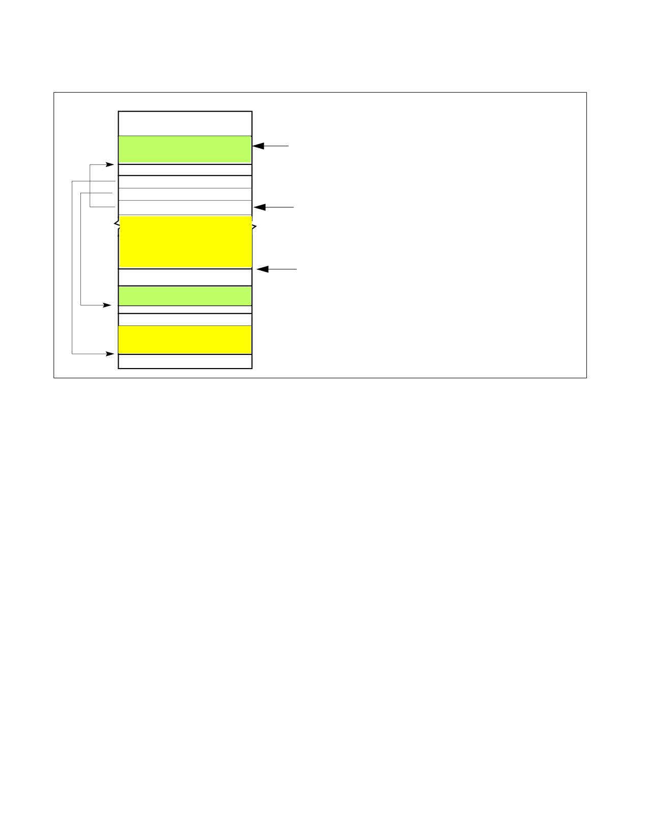
INTEL® PROCESSOR TRACE
Figure
33-1 provides an illustration (not to scale) of the table and associated pointers.
0FF_FFFF _FFFFH
Physical Memory
OutputRegionX
proc_trace_output_offset: IA32_RTIT_OUTPUT_MASK_PTRS.OutputOffset
END=1
TableBaseB
4K
OutputBaseY
64K
OutputBaseX
proc_trace_table_offset:
IA32_RTIT_OUTPUT_MASK_PRS.MaskOrTableOffset<<3
ToPA Table A
proc_trace_table_base: IA32_RTIT_OUTPUT_BASE
OutputRegionY
STOP=1
ToPA Table B
0
Figure 33-1. ToPA Memory Illustration
With the ToPA mechanism, the processor writes packets to the current output region (identified by
proc_trace_table_base and the proc_trace_table_offset). The offset within that region to which the next byte will
be written is identified by proc_trace_output_offset. When that region is filled with packet output (thus
proc_trace_output_offset = RegionSize-1), proc_trace_table_offset is moved to the next ToPA entry,
proc_trace_output_offset is set to 0, and packet writes begin filling the new output region specified by
proc_trace_table_offset.
As packets are written out, each store derives its physical address as follows:
trace_store_phys_addr := Base address from current ToPA table entry +
proc_trace_output_offset
Eventually, the regions represented by all entries in the table may become full, and the final entry of the table is
reached. An entry can be identified as the final entry because it has either the END or STOP attribute. The END
attribute indicates that the address in the entry does not point to another output region, but rather to another ToPA
table. The STOP attribute indicates that tracing will be disabled once the corresponding region is filled. See Table
33-3 and the section that follows for details on STOP.
When an END entry is reached, the processor loads proc_trace_table_base with the base address held in this END
entry, thereby moving the current table pointer to this new table. The proc_trace_table_offset is reset to 0, as is
the proc_trace_output_offset, and packet writes will resume at the base address indicated in the first entry.
If the table has no STOP or END entry, and trace-packet generation remains enabled, eventually the maximum
table size will be reached (proc_trace_table_offset = 0FFFFFF8H). In this case, the proc_trace_table_offset and
proc_trace_output_offset are reset to 0 (wrapping back to the beginning of the current table) once the last output
region is filled.
Vol. 3C
33-11

INTEL® PROCESSOR TRACE
It is important to note that processor updates to the IA32_RTIT_OUTPUT_BASE and
IA32_RTIT_OUTPUT_MASK_PTRS MSRs are asynchronous to instruction execution. Thus, reads of these MSRs
while Intel PT is enabled may return stale values. Like all IA32_RTIT_* MSRs, the values of these MSRs should not
be trusted or saved unless trace packet generation is first disabled by clearing IA32_RTIT_CTL.TraceEn. This
ensures that the output MSR values account for all packets generated to that point, after which the processor will
cease updating the output MSR values until tracing resumes. 1
The processor may cache internally any number of entries from the current table or from tables that it references
(directly or indirectly). If tracing is enabled, the processor may ignore or delay detection of modifications to these
tables. To ensure that table changes are detected by the processor in a predictable manner, software should clear
TraceEn before modifying the current table (or tables that it references) and only then re-enable packet generation.
Single Output Region ToPA Implementation
The first processor generation to implement Intel PT supports only ToPA configurations with a single ToPA entry
followed by an END entry that points back to the first entry (creating one circular output buffer). Such processors
enumerate CPUID.(EAX=14H,ECX=0):ECX.MENTRY[bit 1] = 0 and CPUID.(EAX=14H,ECX=0):ECX.TOPAOUT[bit
0] = 1.
If CPUID.(EAX=14H,ECX=0):ECX.MENTRY[bit 1] = 0, ToPA tables can hold only one output entry, which must be
followed by an END=1 entry which points back to the base of the table. Hence only one contiguous block can be
used as output.
The lone output entry can have INT or STOP set, but nonetheless must be followed by an END entry as described
above. Note that, if INT=1, the PMI will actually be delivered before the region is filled.
ToPA Table Entry Format
The format of ToPA table entries is shown in Figure 33-2. The size of the address field is determined by the
processor’s physical-address width (MAXPHYADDR) in bits, as reported in CPUID.80000008H:EAX[7:0].
63
MAXPHYADDR-1
12 11 10 9
6 5
4
3
2
1
0
Output Region Base Physical Address
9:6 Size
4 : STOP
2 : INT
Reserved
0 : END
Figure 33-2. Layout of ToPA Table Entry
Table 33-3 describes the details of the ToPA table entry fields. If reserved bits are set to 1, an error is signaled.
Table 33-3. ToPA Table Entry Fields
ToPA Entry Field
Description
Output Region
If END=0, this is the base physical address of the output region specified by this entry. Note that all regions
Base Physical
must be aligned based on their size. Thus a 2M region must have bits 20:12 clear. If the region is not properly
Address
aligned, an operational error will be signaled when the entry is reached.
If END=1, this is the 4K-aligned base physical address of the next ToPA table (which may be the base of the cur-
rent table, or the first table in the linked list if a circular buffer is desired). If the processor supports only a single
ToPA output region (see above), this address must be the value currently in the IA32_RTIT_OUTPUT_BASE
MSR.
1. Although WRMSR is a serializing instruction, the execution of WRMSR that forces packet writes by clearing Tra-
ceEn does not itself cause these writes to be globally observed.
33-12
Vol. 3C

INTEL® PROCESSOR TRACE
Table 33-3. ToPA Table Entry Fields (Contd.)
ToPA Entry Field
Description
Size
Indicates the size of the associated output region. Encodings are:
0: 4K, 1: 8K,
2: 16K,
3: 32K,
4: 64K,
5: 128K,
6: 256K,
7: 512K,
8: 1M, 9: 2M,
10: 4M,
11: 8M,
12: 16M,
13: 32M,
14: 64M,
15: 128M
This field is ignored if END=1.
STOP
When the output region indicated by this entry is filled, software should disable packet generation. This will be
accomplished by setting IA32_RTIT_STATUS.Stopped, which clears TriggerEn. This bit must be 0 if END=1; oth-
erwise it is treated as reserved bit violation (see ToPA Errors).
INT
When the output region indicated by this entry is filled, signal Perfmon LVT interrupt.
Note that if both INT and STOP are set in the same entry, the STOP will happen before the INT. Thus the inter-
rupt handler should expect that the IA32_RTIT_STATUS.Stopped bit will be set, and will need to be reset before
tracing can be resumed.
This bit must be 0 if END=1; otherwise it is treated as reserved bit violation (see ToPA Errors).
END
If set, indicates that this is an END entry, and thus the address field points to a table base rather than an output
region base.
If END=1, INT and STOP must be set to 0; otherwise it is treated as reserved bit violation (see ToPA Errors). The
Size field is ignored in this case.
If the processor supports only a single ToPA output region (see above), END must be set in the second table
entry.
ToPA STOP
Each ToPA entry has a STOP bit. If this bit is set, the processor will set the IA32_RTIT_STATUS.Stopped bit when
the corresponding trace output region is filled. This will clear TriggerEn and thereby cease packet generation. See
Section 33.2.8.4 for details on IA32_RTIT_STATUS.Stopped. This sequence is known as “ToPA Stop”.
No TIP.PGD packet will be seen in the output when the ToPA stop occurs, since the disable happens only when the
region is already full. When this occurs, output ceases after the last byte of the region is filled, which may mean
that a packet is cut off in the middle. Any packets remaining in internal buffers are lost and cannot be recovered.
When ToPA stop occurs, the IA32_RTIT_OUTPUT_BASE MSR will hold the base address of the table whose entry
had STOP=1. IA32_RTIT_OUTPUT_MASK_PTRS.MaskOrTableOffset will hold the index value for that entry, and the
IA32_RTIT_OUTPUT_MASK_PTRS.OutputOffset should be set to the size of the region minus one.
Note that this means the offset pointer is pointing to the next byte after the end of the region, a configuration that
would produce an operational error if the configuration remained when tracing is re-enabled with
IA32_RTIT_STATUS.Stopped cleared.
ToPA PMI
Each ToPA entry has an INT bit. If this bit is set, the processor will signal a performance-monitoring interrupt (PMI)
when the corresponding trace output region is filled. This interrupt is not precise, and it is thus likely that writes to
the next region will occur by the time the interrupt is taken.
The following steps should be taken to configure this interrupt:
1. Enable PMI via the LVT Performance Monitor register (at MMIO offset 340H in xAPIC mode; via MSR 834H in
x2APIC mode). See the Intel® 64 and IA-32 Architectures Software Developer’s Manual, Volume 3B, for more
details on this register. For ToPA PMI, set all fields to 0, save for the interrupt vector, which can be selected by
software.
2. Set up an interrupt handler to service the interrupt vector that a ToPA PMI can raise.
3. Set the interrupt flag by executing STI.
4. Set the INT bit in the ToPA entry of interest and enable packet generation, using the ToPA output option. Thus,
TraceEn=ToPA=1 in the IA32_RTIT_CTL MSR.
Once the INT region has been filled with packet output data, the interrupt will be signaled. This PMI can be distin-
guished from others by checking bit 55 (Trace_ToPA_PMI) of the IA32_PERF_GLOBAL_STATUS MSR (MSR 38EH).
Once the ToPA PMI handler has serviced the relevant buffer, writing 1 to bit 55 of the MSR at 390H
(IA32_GLOBAL_STATUS_RESET) clears IA32_PERF_GLOBAL_STATUS.Trace_ToPA_PMI.
Vol. 3C
33-13
INTEL® PROCESSOR TRACE
Intel PT is not frozen on PMI, and thus the interrupt handler will be traced (though filtering can prevent this). The
Freeze_Perfmon_on_PMI and Freeze_LBRs_on_PMI settings in IA32_DEBUGCTL will be applied on ToPA PMI just as
on other PMIs, and hence Perfmon counters are frozen.
Assuming the PMI handler wishes to read any buffered packets for persistent output, or wishes to modify any Intel
PT MSRs, software should first disable packet generation by clearing TraceEn. This ensures that all buffered packets
are written to memory and avoids tracing of the PMI handler. The configuration MSRs can then be used to deter-
mine where tracing has stopped. If packet generation is disabled by the handler, it should then be manually re-
enabled before the IRET if continued tracing is desired.
In rare cases, it may be possible to trigger a second ToPA PMI before the first is handled. This can happen if another
ToPA region with INT=1 is filled before, or shortly after, the first PMI is taken, perhaps due to EFLAGS.IF being
cleared for an extended period of time. This can manifest in two ways: either the second PMI is triggered before the
first is taken, and hence only one PMI is taken, or the second is triggered after the first is taken, and thus will be
taken when the handler for the first completes. Software can minimize the likelihood of the second case by clearing
TraceEn at the beginning of the PMI handler. Further, it can detect such cases by then checking the Interrupt
Request Register (IRR) for PMI pending, and checking the ToPA table base and off-set pointers (in
IA32_RTIT_OUTPUT_BASE and IA32_RTIT_OUTPUT_MASK_PTRS) to see if multiple entries with INT=1 have been
filled.
PMI Preservation
In some cases a ToPA PMI may be taken after completion of an XSAVES instruction that saves Intel PT state, and in
such cases any modification of Intel PT MSRs within the PMI handler will not persist when the saved Intel PT context
is later restored with XRSTORS. To account for such a scenario, the PMI Preservation feature has been added.
Support for this feature is indicated by CPUID.(EAX=14H, ECX=0):EBX[bit 6].
When IA32_RTIT_CTL.InjectPsbPmiOnEnable[56] = 1, PMI preservation is enabled. When a ToPA region with
INT=1 is filled, a PMI is pended and the new IA32_RTIT_STATUS.PendToPAPMI[7] is set to 1. If this bit is set when
Intel PT is enabled, such that IA32_RTIT_CTL.TraceEn[0] transitions from 0 to 1, a ToPA PMI is pended. This
behavior ensures that any ToPA PMI that is pended during XSAVES, and hence can't be properly handled, will be re-
pended when the saved PT state is restored.
When this feature is enabled, the PMI handler should take the following actions:
1. Ignore ToPA PMIs that are taken when TraceEn = 0. This indicates that the PMI was pended during Intel PT
disable, and the PendToPAPMI flag will ensure that the PMI is re-pended once Intel PT is re-enabled in the same
context. For this reason, the PendToPAPMI bit should be left set to 1.
2. If TraceEn=1 and the PMI can be properly handled, clear the new PendTopaPMI bit. This will ensure that
additional, spurious ToPA PMIs are not taken. It is required that PendToPAPMI is cleared before the PMI LVT
mask is cleared in the APIC, and before any clearing of either LBRS_FROZEN or COUNTERS_FROZEN in
IA32_PERF_GLOBAL_STATUS.
ToPA PMI and Single Output Region ToPA Implementation
A processor that supports only a single ToPA output region implementation (such that only one output region is
supported; see above) will attempt to signal a ToPA PMI interrupt before the output wraps and overwrites the top
of the buffer. To support this functionality, the PMI handler should disable packet generation as soon as possible.
Due to PMI skid, it is possible that, in rare cases, the wrap will have occurred before the PMI is delivered. Software
can avoid this by setting the STOP bit in the ToPA entry (see Table 33-3); this will disable tracing once the region is
filled, and no wrap will occur. This approach has the downside of disabling packet generation so that some of the
instructions that led up to the PMI will not be traced. If the PMI skid is significant enough to cause the region to fill
and tracing to be disabled, the PMI handler will need to clear the IA32_RTIT_STATUS.Stopped indication before
tracing can resume.
33-14
Vol. 3C

INTEL® PROCESSOR TRACE
ToPA PMI and XSAVES/XRSTORS State Handling
In some cases the ToPA PMI may be taken after completion of an XSAVES instruction that switches Intel PT state,
and in such cases any modification of Intel PT MSRs within the PMI handler will not persist when the saved Intel PT
context is later restored with XRSTORS. To account for such a scenario, it is recommended that the Intel PT output
configuration be modified by altering the ToPA tables themselves, rather than the Intel PT output MSRs. On proces-
sors that support PMI preservation (CPUID.(EAX=14H, ECX=0):EBX[bit 6] = 1), setting IA32_RTIT_CTL.InjectPsb-
PmiOnEnable[56] = 1 will ensure that a PMI that is pending at the time PT is disabled will be recorded by setting
IA32_RTIT_STATUS.PendTopaPMI[7] = 1. A PMI will then be pended when the saved PT context is later restored.
Table 33-4 depicts a recommended PMI handler algorithm for managing multi-region ToPA output and handling
ToPA PMIs that may arrive between XSAVES and XRSTORS, if PMI preservation is not in use. This algorithm is flex-
ible to allow software to choose between adding entries to the current ToPA table, adding a new ToPA table, or using
the current ToPA table as a circular buffer. It assumes that the ToPA entry that triggers the PMI is not the last entry
in the table, which is the recommended treatment.
Table 33-4. Algorithm to Manage Intel PT ToPA PMI and XSAVES/XRSTORS
Pseudo Code Flow
IF (IA32_PERF_GLOBAL_STATUS.ToPA)
Save IA32_RTIT_CTL value;
IF ( IA32_RTIT_CTL.TraceEN )
Disable Intel PT by clearing TraceEn;
FI;
IF ( there is space available to grow the current ToPA table )
Add one or more ToPA entries after the last entry in the ToPA table;
Point new ToPA entry address field(s) to new output region base(s);
ELSE
Modify an upcoming ToPA entry in the current table to have END=1;
IF (output should transition to a new ToPA table )
Point the address of the “END=1” entry of the current table to the new table base;
ELSE
/* Continue to use the current ToPA table, make a circular. */
Point the address of the “END=1”l entry to the base of the current table;
Modify the ToPA entry address fields for filled output regions to point to new, unused output regions;
/* Filled regions are those with index in the range of 0 to (IA32_RTIT_MASK_PTRS.MaskOrTableOffset -1). */
FI;
FI;
Restore saved IA32_RTIT_CTL.value;
FI;
ToPA Errors
When a malformed ToPA entry is found, an operational error results (see Section 33.3.10). A malformed entry
can be any of the following:
1. ToPA entry reserved bit violation.
This describes cases where a bit marked as reserved in Section 33.2.7.2 above is set to 1.
2. ToPA alignment violation.
This includes cases where illegal ToPA entry base address bits are set to 1:
a. ToPA table base address is not 4KB-aligned. The table base can be from a WRMSR to
IA32_RTIT_OUTPUT_BASE, or from a ToPA entry with END=1.
b. ToPA entry base address is not aligned to the ToPA entry size (e.g., a 2MB region with base address[20:12]
not equal to 0), for ToPA entries with END=0.
c. ToPA entry base address sets upper physical address bits not supported by the processor.
Vol. 3C
33-15

INTEL® PROCESSOR TRACE
3. Illegal ToPA Output Offset.
IA32_RTIT_OUTPUT_MASK_PTRS.OutputOffset is greater than or equal to the size of the current ToPA output
region size.
4. ToPA rules violations.
These are similar to ToPA entry reserved bit violations; they are cases when a ToPA entry is encountered with
illegal field combinations. They include the following:
a. Setting the STOP or INT bit on an entry with END=1.
b. Setting the END bit in entry 0 of a ToPA table.
c. On processors that support only a single ToPA entry (see above), two additional illegal settings apply:
i) ToPA table entry 1 with END=0.
ii) ToPA table entry 1 with base address not matching the table base.
In all cases, the error will be logged by setting IA32_RTIT_STATUS.Error, thereby disabling tracing when the prob-
lematic ToPA entry is reached (when proc_trace_table_offset points to the entry containing the error). Any packet
bytes that are internally buffered when the error is detected may be lost.
Note that operational errors may also be signaled due to attempts to access restricted memory. See Section
33.2.7.4 for details.
A tracing software have a range of flexibility using ToPA to manage the interaction of Intel PT with application
buffers, see Section 33.4.2.26.
33.2.7.3 Trace Transport Subsystem
When IA32_RTIT_CTL.FabricEn is set, the IA32_RTIT_CTL.ToPA bit is ignored, and trace output is written to the
trace transport subsystem. The endpoints of this transport are platform-specific, and details of configuration
options should refer to the specific platform documentation. The FabricEn bit is available to be set if
CPUID(EAX=14H,ECX=0):EBX[bit 3] = 1.
33.2.7.4 Restricted Memory Access
Packet output cannot be directed to any regions of memory that are restricted by the platform. In particular, all
memory accesses on behalf of packet output are checked against the SMRR regions. If there is any overlap with
these regions, trace data collection will not function properly. Exact processor behavior is implementation-depen-
dent; Table 33-5 summarizes several scenarios.
Table 33-5. Behavior on Restricted Memory Access
Scenario
Description
ToPA output region
Stores to the restricted memory region will be dropped, and that packet data will be lost. Any attempt to read
overlaps with
from that restricted region will return all 1s. The processor also may signal an error (Section 33.3.10) and dis-
SMRR
able tracing when the output pointer reaches the restricted region. If packet generation remains enabled, then
packet output may continue once stores are no longer directed to restricted memory (on wrap, or if the output
region is larger than the restricted memory region).
ToPA table overlaps
The processor will signal an error (Section 33.3.10) and disable tracing when the ToPA write pointer (IA32_R-
with SMRR
TIT_OUTPUT_BASE + proc_trace_table_offset) enters the restricted region.
It should also be noted that packet output should not be routed to the 4KB APIC MMIO region, as defined by the
IA32_APIC_BASE MSR. For details about the APIC, refer to the Intel® 64 and IA-32 Architectures Software Devel-
oper’s Manual, Volume 3A. No error is signaled for this case.
Modifications to Restricted Memory Regions
It is recommended that software disable packet generation before modifying the SMRRs to change the scope of the
SMRR regions. This is because the processor reserves the right to cache any number of ToPA table entries inter-
nally, after checking them against restricted memory ranges. Once cached, the entries will not be checked again,
meaning one could potentially route packet output to a newly restricted region. Software can ensure that any
cached entries are written to memory by clearing IA32_RTIT_CTL.TraceEn.
33-16
Vol. 3C

INTEL® PROCESSOR TRACE
33.2.8 Enabling and Configuration MSRs
33.2.8.1 General Considerations
Trace packet generation is enabled and configured by a collection of model-specific registers (MSRs), which are
detailed below. Some notes on the configuration MSR behavior:
• If Intel Processor Trace is not supported by the processor (see Section 33.3.1), RDMSR or WRMSR of the
IA32_RTIT_* MSRs will cause #GP.
• A WRMSR to any of the IA32_RTIT_* configuration MSRs while packet generation is enabled
(IA32_RTIT_CTL.TraceEn=1) will generate a #GP exception. Packet generation must be disabled before the
configuration MSRs can be changed.
Note: Software may write the same value back to IA32_RTIT_CTL without #GP, even if TraceEn=1.
• All configuration MSRs for Intel PT are duplicated per logical processor
• For each configuration MSR, any MSR write that attempts to change bits marked reserved, or utilize encodings
marked reserved, will cause a #GP fault.
• All configuration MSRs for Intel PT are cleared on a warm or cold RESET.
— If CPUID.(EAX=14H, ECX=0):EBX[bit 2] = 1, only the TraceEn bit is cleared on warm RESET; though this
may have the impact of clearing other bits in IA32_RTIT_STATUS. Other MSR values of the trace configu-
ration MSRs are preserved on warm RESET.
• The semantics of MSR writes to trace configuration MSRs in this chapter generally apply to explicit WRMSR to
these registers, using VMexit or VM entry MSR load list to these MSRs, XRSTORS with requested feature bit
map including XSAVE map component of state_8 (corresponding to IA32_XSS[bit 8]), and the write to
IA32_RTIT_CTL.TraceEn by XSAVES (Section 33.3.5.2).
33.2.8.2 IA32_RTIT_CTL MSR
IA32_RTIT_CTL, at address 570H, is the primary enable and control MSR for trace packet generation. Bit positions
are listed in Table 33-6.
Table 33-6. IA32_RTIT_CTL MSR
Position
Bit Name
At Reset
Bit Description
0
TraceEn
0
If 1, enables tracing; else tracing is disabled.
When this bit transitions from 1 to 0, all buffered packets are flushed out of internal buffers.
A further store, fence, or architecturally serializing instruction may be required to ensure that
packet data can be observed at the trace endpoint. See Section 33.2.8.3 for details of
enabling and disabling packet generation.
Note that the processor will clear this bit on #SMI (Section 33.2.9.3) and warm reset. Other
MSR bits of IA32_RTIT_CTL (and other trace configuration MSRs) are not impacted by these
events.
1
CYCEn
0
0: Disables CYC Packet (see Section 33.4.2.14).
1: Enables CYC Packet.
This bit is reserved if CPUID.(EAX=14H, ECX=0):EBX[bit 1] = 0.
2
OS
0
0: Packet generation is disabled when CPL = 0.
1: Packet generation may be enabled when CPL = 0.
3
User
0
0: Packet generation is disabled when CPL > 0.
1: Packet generation may be enabled when CPL > 0.
4
PwrEvtEn
0
0: Power Event Trace packets are disabled.
1: Power Event Trace packets are enabled (see Section 33.2.3, “Power Event Tracing”).
Vol. 3C
33-17

INTEL® PROCESSOR TRACE
Table 33-6. IA32_RTIT_CTL MSR (Contd.)
Position
Bit Name
At Reset
Bit Description
5
FUPonPTW
0
0: PTW packets are not followed by FUPs.
1: PTW packets are followed by FUPs.
This bit is reserved when CPUID.(EAX=14H, ECX=0):EBX[bit 4] (“PTWRITE Supported”) is 0.
6
FabricEn
0
0: Trace output is directed to the memory subsystem, mechanism depends on
IA32_RTIT_CTL.ToPA.
1: Trace output is directed to the trace transport subsystem, IA32_RTIT_CTL.ToPA is ignored.
This bit is reserved if CPUID.(EAX=14H, ECX=0):ECX[bit 3] = 0.
7
CR3Filter
0
0: Disables CR3 filtering.
1: Enables CR3 filtering.
This bit is reserved if CPUID.(EAX=14H, ECX=0):EBX[bit 0] (“CR3 Filtering Support”) is 0.
8
ToPA
0
0: Single-range output scheme enabled if CPUID.(EAX=14H, ECX=0):ECX.SNGLRGNOUT[bit 2]
= 1 and IA32_RTIT_CTL.FabricEn=0.
1: ToPA output scheme enabled (see Section 33.2.7.2) if CPUID.(EAX=14H,
ECX=0):ECX.TOPA[bit 0] = 1, and IA32_RTIT_CTL.FabricEn=0.
Note: WRMSR to IA32_RTIT_CTL that sets TraceEn but clears this bit and FabricEn would
cause #GP, if CPUID.(EAX=14H, ECX=0):ECX.SNGLRGNOUT[bit 2] = 0.
WRMSR to IA32_RTIT_CTL that sets this bit causes #GP, if CPUID.(EAX=14H,
ECX=0):ECX.TOPA[bit 0] = 0.
9
MTCEn
0
0: Disables MTC Packet (see Section 33.4.2.16).
1: Enables MTC Packet.
This bit is reserved if CPUID.(EAX=14H, ECX=0):EBX[bit 3] = 0.
10
TSCEn
0
0: Disable TSC packets.
1: Enable TSC packets (see Section 33.4.2.11).
11
DisRETC
0
0: Enable RET compression.
1: Disable RET compression (see Section 33.2.1.2).
12
PTWEn
0
0: PTWRITE packet generation disabled.
1: PTWRITE packet generation enabled (see Table 33-40 “PTW Packet Definition”).
This bit is reserved when CPUID.(EAX=14H, ECX=0):EBX[bit 4] (“PTWRITE Supported”) is 0.
13
BranchEn
0
0: Disable COFI-based packets.
1: Enable COFI-based packets: FUP, TIP, TIP.PGE, TIP.PGD, TNT, MODE.Exec, MODE.TSX.
See Section 33.2.6.4 for details on BranchEn.
17:14
MTCFreq
0
Defines MTC packet Frequency, which is based on the core crystal clock, or Always Running
Timer (ART). MTC will be sent each time the selected ART bit toggles. The following Encodings
are defined:
0: ART(0), 1: ART(1), 2: ART(2), 3: ART(3), 4: ART(4), 5: ART(5), 6: ART(6), 7: ART(7),
8: ART(8), 9: ART(9), 10: ART(10), 11: ART(11), 12: ART(12), 13: ART(13), 14: ART(14), 15:
ART(15)
Software must use CPUID to query the supported encodings in the processor, see Section
33.3.1. Use of unsupported encodings will result in a #GP fault. This field is reserved if
CPUID.(EAX=14H, ECX=0):EBX[bit 3] = 0.
18
Reserved
0
Must be 0.
33-18
Vol. 3C