Intel 64 and IA-32 Architectures. Software Developer’s Manual (Collection, 2023) - page 54

Intel® 64 and IA-32 Architectures
Software Developer’s Manual
Volume 3B:
System Programming Guide, Part 2
NOTE: The Intel® 64 and IA-32 Architectures Software Developer's Manual consists of ten volumes:
Basic Architecture, Order Number 253665; Instruction Set Reference, A-L, Order Number 253666;
Instruction Set Reference, M-U, Order Number 253667; Instruction Set Reference, V, Order Number
326018; Instruction Set Reference, W-Z, Order Number 334569; System Programming Guide, Part 1,
Order Number
253668; System Programming Guide, Part
2, Order Number
253669; System
Programming Guide, Part 3, Order Number 326019; System Programming Guide, Part 4, Order Number
332831; Model-Specific Registers, Order Number 335592. Refer to all ten volumes when evaluating
your design needs.
Order Number: 253669-081US
September 2023

CHAPTER 15
POWER AND THERMAL MANAGEMENT
This chapter describes facilities of Intel 64 and IA-32 architecture used for power management and thermal moni-
toring.
15.1
ENHANCED INTEL SPEEDSTEP® TECHNOLOGY
Enhanced Intel SpeedStep® Technology was introduced in the Pentium M processor. The technology enables the
management of processor power consumption via performance state transitions. These states are defined as
discrete operating points associated with different voltages and frequencies.
Enhanced Intel SpeedStep Technology differs from previous generations of Intel SpeedStep® Technology in two
ways:
• Centralization of the control mechanism and software interface in the processor by using model-specific
registers.
• Reduced hardware overhead; this permits more frequent performance state transitions.
Previous generations of the Intel SpeedStep Technology require processors to be a deep sleep state, holding off bus
master transfers for the duration of a performance state transition. Performance state transitions under the
Enhanced Intel SpeedStep Technology are discrete transitions to a new target frequency.
Support is indicated by CPUID, using ECX feature bit 07. Enhanced Intel SpeedStep Technology is enabled by
setting IA32_MISC_ENABLE MSR, bit 16. On reset, bit 16 of IA32_MISC_ENABLE MSR is cleared.
15.1.1 Software Interface For Initiating Performance State Transitions
State transitions are initiated by writing a 16-bit value to the IA32_PERF_CTL register, see Figure 15-2. If a transi-
tion is already in progress, transition to a new value will subsequently take effect.
Reads of IA32_PERF_CTL determine the last targeted operating point. The current operating point can be read from
IA32_PERF_STATUS. IA32_PERF_STATUS is updated dynamically.
The 16-bit encoding that defines valid operating points is model-specific. Applications and performance tools are
not expected to use either IA32_PERF_CTL or IA32_PERF_STATUS and should treat both as reserved. Performance
monitoring tools can access model-specific events and report the occurrences of state transitions.
15.2
P-STATE HARDWARE COORDINATION
The Advanced Configuration and Power Interface (ACPI) defines performance states (P-states) that are used to
facilitate system software’s ability to manage processor power consumption. Different P-states correspond to
different performance levels that are applied while the processor is actively executing instructions. Enhanced Intel
SpeedStep Technology supports P-states by providing software interfaces that control the operating frequency and
voltage of a processor.
With multiple processor cores residing in the same physical package, hardware dependencies may exist for a
subset of logical processors on a platform. These dependencies may impose requirements that impact the coordi-
nation of P-state transitions. As a result, multi-core processors may require an OS to provide additional software
support for coordinating P-state transitions for those subsets of logical processors.
ACPI firmware can choose to expose P-states as dependent and hardware-coordinated to OS power management
(OSPM) policy. To support OSPMs, multi-core processors must have additional built-in support for P-state hardware
coordination and feedback.
Intel 64 and IA-32 processors with dependent P-states amongst a subset of logical processors permit hardware
coordination of P-states and provide a hardware-coordination feedback mechanism using IA32_MPERF MSR and
Vol. 3B
15-1

POWER AND THERMAL MANAGEMENT
IA32_APERF MSR. See Figure 15-1 for an overview of the two 64-bit MSRs and the bullets below for a detailed
description.
63
0
63
0
IA32_MPERF (Addr: E7H)
IA32_APERF (Addr: E8H)
Figure 15-1. IA32_MPERF MSR and IA32_APERF MSR for P-state Coordination
• Use CPUID to check the P-State hardware coordination feedback capability bit. CPUID.06H.ECX[Bit 0] = 1
indicates IA32_MPERF MSR and IA32_APERF MSR are present.
• IA32_MPERF MSR (E7H) increments in proportion to a fixed frequency, which is configured when the processor
is booted.
• IA32_APERF MSR (E8H) increments in proportion to actual performance, while accounting for hardware coordi-
nation of P-state and TM1/TM2; or software initiated throttling.
• The MSRs are per logical processor; they measure performance only when the targeted processor is in the C0
state.
• Only the IA32_APERF/IA32_MPERF ratio is architecturally defined; software should not attach meaning to the
content of the individual of IA32_APERF or IA32_MPERF MSRs.
• When either MSR overflows, both MSRs are reset to zero and continue to increment.
• Both MSRs are full 64-bits counters. Each MSR can be written to independently. However, software should
follow the guidelines illustrated in Example 15-1.
If P-states are exposed by the BIOS as hardware coordinated, software is expected to confirm processor support
for P-state hardware coordination feedback and use the feedback mechanism to make P-state decisions. The OSPM
is expected to either save away the current MSR values (for determination of the delta of the counter ratio at a later
time) or reset both MSRs (execute WRMSR with 0 to these MSRs individually) at the start of the time window used
for making the P-state decision. When not resetting the values, overflow of the MSRs can be detected by checking
whether the new values read are less than the previously saved values.
Example 15-1 demonstrates steps for using the hardware feedback mechanism provided by IA32_APERF MSR and
IA32_MPERF MSR to determine a target P-state.
Example 15-1. Determine Target P-state From Hardware Coordinated Feedback
DWORD PercentBusy; // Percentage of processor time not idle.
// Measure “PercentBusy“ during previous sampling window.
// Typically, “PercentBusy“ is measure over a time scale suitable for
// power management decisions
//
// RDMSR of MCNT and ACNT should be performed without delay.
// Software needs to exercise care to avoid delays between
// the two RDMSRs (for example, interrupts).
MCNT = RDMSR(IA32_MPERF);
ACNT = RDMSR(IA32_APERF);
// PercentPerformance indicates the percentage of the processor
// that is in use. The calculation is based on the PercentBusy,
// that is the percentage of processor time not idle and the P-state
// hardware coordinated feedback using the ACNT/MCNT ratio.
// Note that both values need to be calculated over the same
15-2
Vol. 3B
POWER AND THERMAL MANAGEMENT
// time window.
PercentPerformance = PercentBusy * (ACNT/MCNT);
// This example does not cover the additional logic or algorithms
// necessary to coordinate multiple logical processors to a target P-state.
TargetPstate = FindPstate(PercentPerformance);
if (TargetPstate ≠ currentPstate) {
SetPState(TargetPstate);
}
// WRMSR of MCNT and ACNT should be performed without delay.
// Software needs to exercise care to avoid delays between
// the two WRMSRs (for example, interrupts).
WRMSR(IA32_MPERF, 0);
WRMSR(IA32_APERF, 0);
15.3
SYSTEM SOFTWARE CONSIDERATIONS AND OPPORTUNISTIC PROCESSOR
PERFORMANCE OPERATION
An Intel 64 processor may support a form of processor operation that takes advantage of design headroom to
opportunistically increase performance. The Intel® Turbo Boost Technology can convert thermal headroom into
higher performance across multi-threaded and single-threaded workloads. The Intel® Dynamic Acceleration Tech-
nology feature can convert thermal headroom into higher performance if only one thread is active.
15.3.1 Intel® Dynamic Acceleration Technology
The Intel Core 2 Duo processor T 7700 introduces Intel Dynamic Acceleration Technology. Intel Dynamic Accelera-
tion Technology takes advantage of thermal design headroom and opportunistically allows a single core to operate
at a higher performance level when the operating system requests increased performance.
15.3.2 System Software Interfaces for Opportunistic Processor Performance Operation
Opportunistic processor performance operation, applicable to Intel Dynamic Acceleration Technology and Intel®
Turbo Boost Technology, has the following characteristics:
• A transition from a normal state of operation (e.g., Intel Dynamic Acceleration Technology/Turbo mode
disengaged) to a target state is not guaranteed, but may occur opportunistically after the corresponding enable
mechanism is activated, the headroom is available and certain criteria are met.
• The opportunistic processor performance operation is generally transparent to most application software.
• System software (BIOS and Operating system) must be aware of hardware support for opportunistic processor
performance operation and may need to temporarily disengage opportunistic processor performance operation
when it requires more predictable processor operation.
• When opportunistic processor performance operation is engaged, the OS should use hardware coordination
feedback mechanisms to prevent un-intended policy effects if it is activated during inappropriate situations.
15.3.2.1 Discover Hardware Support and Enabling of Opportunistic Processor Performance Operation
If an Intel 64 processor has hardware support for opportunistic processor performance operation, the power-on
default state of IA32_MISC_ENABLE[38] indicates the presence of such hardware support. For Intel 64 processors
that support opportunistic processor performance operation, the default value is 1, indicating its presence. For
processors that do not support opportunistic processor performance operation, the default value is 0. The power-
Vol. 3B
15-3

POWER AND THERMAL MANAGEMENT
on default value of IA32_MISC_ENABLE[38] allows BIOS to detect the presence of hardware support of opportu-
nistic processor performance operation.
IA32_MISC_ENABLE[38] is shared across all logical processors in a physical package. It is written by BIOS during
platform initiation to enable/disable opportunistic processor performance operation in conjunction of OS power
management capabilities, see Section 15.3.2.2. BIOS can set IA32_MISC_ENABLE[38] with 1 to disable opportu-
nistic processor performance operation; it must clear the default value of IA32_MISC_ENABLE[38] to 0 to enable
opportunistic processor performance operation. OS and applications must use CPUID leaf 06H if it needs to detect
processors that have opportunistic processor performance operation enabled.
When CPUID is executed with EAX = 06H on input, Bit 1 of EAX in Leaf 06H (i.e., CPUID.06H:EAX[1]) indicates
opportunistic processor performance operation, such as Intel Dynamic Acceleration Technology, has been enabled
by BIOS.
Opportunistic processor performance operation can be disabled by setting bit 38 of IA32_MISC_ENABLE. This
mechanism is intended for BIOS only. If IA32_MISC_ENABLE[38] is set, CPUID.06H:EAX[1] will return 0.
15.3.2.2 OS Control of Opportunistic Processor Performance Operation
There may be phases of software execution in which system software cannot tolerate the non-deterministic aspects
of opportunistic processor performance operation. For example, when calibrating a real-time workload to make a
CPU reservation request to the OS, it may be undesirable to allow the possibility of the processor delivering
increased performance that cannot be sustained after the calibration phase.
System software can temporarily disengage opportunistic processor performance operation by setting bit 32 of the
IA32_PERF_CTL MSR (0199H), using a read-modify-write sequence on the MSR. The opportunistic processor
performance operation can be re-engaged by clearing bit 32 in IA32_PERF_CTL MSR, using a read-modify-write
sequence. The DISENAGE bit in IA32_PERF_CTL is not reflected in bit 32 of the IA32_PERF_STATUS MSR (0198H),
and it is not shared between logical processors in a physical package. In order for OS to engage Intel Dynamic
Acceleration Technology/Turbo mode, the BIOS must:
• Enable opportunistic processor performance operation, as described in Section 15.3.2.1.
• Expose the operating points associated with Intel Dynamic Acceleration Technology/Turbo mode to the OS.
63
33 32 31
16 15
0
Reserved
Reserved
Intel® Dynamic Acceleration Technology / Turbo Engage Bit
(Used to Disengage Feature)
Enhanced Intel Speedstep® Technology Transition Target
Figure 15-2. IA32_PERF_CTL Register
15.3.2.3 Required Changes to OS Power Management P-State Policy
Intel Dynamic Acceleration Technology and Intel Turbo Boost Technology can provide opportunistic performance
greater than the performance level corresponding to the Processor Base frequency of the processor (see CPUID’s
processor frequency information). System software can use a pair of MSRs to observe performance feedback. Soft-
ware must query for the presence of IA32_APERF and IA32_MPERF (see Section 15.2). The ratio between
IA32_APERF and IA32_MPERF is architecturally defined and a value greater than unity indicates performance
increase occurred during the observation period due to Intel Dynamic Acceleration Technology. Without incorpo-
rating such performance feedback, the target P-state evaluation algorithm can result in a non-optimal P-state
target.
15-4
Vol. 3B

POWER AND THERMAL MANAGEMENT
There are other scenarios under which OS power management may want to disable Intel Dynamic Acceleration
Technology, some of these are listed below:
• When engaging ACPI defined passive thermal management, it may be more effective to disable Intel Dynamic
Acceleration Technology for the duration of passive thermal management.
• When the user has indicated a policy preference of power savings over performance, OS power management
may want to disable Intel Dynamic Acceleration Technology while that policy is in effect.
15.3.3 Intel® Turbo Boost Technology
Intel Turbo Boost Technology is supported in Intel Core i7 processors and Intel Xeon processors based on Nehalem
microarchitecture. It uses the same principle of leveraging thermal headroom to dynamically increase processor
performance for single-threaded and multi-threaded/multi-tasking environment. The programming interface
described in Section 15.3.2 also applies to Intel Turbo Boost Technology.
15.3.4 Performance and Energy Bias Hint Support
Intel 64 processors may support additional software hint to guide the hardware heuristic of power management
features to favor increasing dynamic performance or conserve energy consumption.
Software can detect the processor's capability to support the performance-energy bias preference hint by exam-
ining bit 3 of ECX in CPUID leaf 6. The processor supports this capability if CPUID.06H:ECX.SETBH[bit 3] is set and
it also implies the presence of a new architectural MSR called IA32_ENERGY_PERF_BIAS (1B0H).
Software can program the lowest four bits of IA32_ENERGY_PERF_BIAS MSR with a value from 0 - 15. The values
represent a sliding scale, where a value of 0 (the default reset value) corresponds to a hint preference for highest
performance and a value of 15 corresponds to the maximum energy savings. A value of 7 roughly translates into a
hint to balance performance with energy consumption.
63
4 3
0
Reserved
Energy Policy Preference Hint
Figure 15-3. IA32_ENERGY_PERF_BIAS Register
The layout of IA32_ENERGY_PERF_BIAS is shown in Figure 15-3. The scope of IA32_ENERGY_PERF_BIAS is per
logical processor, which means that each of the logical processors in the package can be programmed with a
different value. This may be especially important in virtualization scenarios, where the performance / energy
requirements of one logical processor may differ from the other. Conflicting “hints” from various logical processors
at higher hierarchy level will be resolved in favor of performance over energy savings.
Software can use whatever criteria it sees fit to program the MSR with an appropriate value. However, the value
only serves as a hint to the hardware and the actual impact on performance and energy savings is model specific.
15.4
HARDWARE-CONTROLLED PERFORMANCE STATES (HWP)
Intel processors may contain support for Hardware-Controlled Performance States (HWP), which autonomously
selects performance states while utilizing OS supplied performance guidance hints. The Enhanced Intel Speed-
Step® Technology provides a means for the OS to control and monitor discrete frequency-based operating points
via the IA32_PERF_CTL and IA32_PERF_STATUS MSRs.
Vol. 3B
15-5

POWER AND THERMAL MANAGEMENT
In contrast, HWP is an implementation of the ACPI-defined Collaborative Processor Performance Control (CPPC),
which specifies that the platform enumerates a continuous, abstract unit-less, performance value scale that is not
tied to a specific performance state / frequency by definition. While the enumerated scale is roughly linear in terms
of a delivered integer workload performance result, the OS is required to characterize the performance value range
to comprehend the delivered performance for an applied workload.
When HWP is enabled, the processor autonomously selects performance states as deemed appropriate for the
applied workload and with consideration of constraining hints that are programmed by the OS. These OS-provided
hints include minimum and maximum performance limits, preference towards energy efficiency or performance,
and the specification of a relevant workload history observation time window. The means for the OS to override
HWP's autonomous selection of performance state with a specific desired performance target is also provided,
however, the effective frequency delivered is subject to the result of energy efficiency and performance optimiza-
tions.
15.4.1 HWP Programming Interfaces
The programming interfaces provided by HWP include the following:
• The CPUID instruction allows software to discover the presence of HWP support in an Intel processor. Specifi-
cally, execute CPUID instruction with EAX=06H as input will return 5 bit flags covering the following aspects in
bits 7 through 11 of CPUID.06H:EAX:
— Availability of HWP baseline resource and capability, CPUID.06H:EAX[bit 7]: If this bit is set, HWP provides
several new architectural MSRs: IA32_PM_ENABLE, IA32_HWP_CAPABILITIES, IA32_HWP_REQUEST,
IA32_HWP_STATUS.
— Availability of HWP Notification upon dynamic Guaranteed Performance change, CPUID.06H:EAX[bit 8]: If
this bit is set, HWP provides IA32_HWP_INTERRUPT MSR to enable interrupt generation due to dynamic
Performance changes and excursions.
— Availability of HWP Activity window control, CPUID.06H:EAX[bit 9]: If this bit is set, HWP allows software to
program activity window in the IA32_HWP_REQUEST MSR.
— Availability of HWP energy/performance preference control, CPUID.06H:EAX[bit 10]: If this bit is set, HWP
allows software to set an energy/performance preference hint in the IA32_HWP_REQUEST MSR.
— Availability of HWP package level control, CPUID.06H:EAX[bit 11]:If this bit is set, HWP provides the
IA32_HWP_REQUEST_PKG MSR to convey OS Power Management’s control hints for all logical processors
in the physical package.
Table 15-1. Architectural and Non-Architectural MSRs Related to HWP
Address
Architectural
Register Name
Description
770H
Y
IA32_PM_ENABLE
Enable/Disable HWP.
771H
Y
IA32_HWP_CAPABILITIES
Enumerates the HWP performance range (static and dynamic).
772H
Y
IA32_HWP_REQUEST_PKG
Conveys OSPM's control hints (Min, Max, Activity Window, Energy
Performance Preference, Desired) for all logical processor in the
physical package.
773H
Y
IA32_HWP_INTERRUPT
Controls HWP native interrupt generation (Guaranteed Performance
changes, excursions).
774H
Y
IA32_HWP_REQUEST
Conveys OSPM's control hints (Min, Max, Activity Window, Energy
Performance Preference, Desired) for a single logical processor.
775H
Y
IA32_HWP_PECI_REQUEST_INFO
Conveys embedded system controller requests to override some of
the OS HWP Request settings via the PECI mechanism.
777H
Y
IA32_HWP_STATUS
Status bits indicating changes to Guaranteed Performance and
excursions to Minimum Performance.
19CH
Y
IA32_THERM_STATUS[bits 15:12]
Conveys reasons for performance excursions.
64EH
N
MSR_PPERF
Productive Performance Count.
15-6
Vol. 3B

POWER AND THERMAL MANAGEMENT
• Additionally, HWP may provide a non-architectural MSR, MSR_PPERF, which provides a quantitative metric to
software of hardware’s view of workload scalability. This hardware’s view of workload scalability is implemen-
tation specific.
15.4.2 Enabling HWP
The layout of the IA32_PM_ENABLE MSR is shown in Figure 15-4. The bit fields are described below:
63
1 0
Reserved
HWP_ENABLE
Figure 15-4. IA32_PM_ENABLE MSR
• HWP_ENABLE (bit 0, R/W1Once) — Software sets this bit to enable HWP with autonomous selection of
processor P-States. When set, the processor will disregard input from the legacy performance control interface
(IA32_PERF_CTL). Note this bit can only be enabled once from the default value. Once set, writes to the
HWP_ENABLE bit are ignored. Only RESET will clear this bit. Default = zero (0).
• Bits 63:1 are reserved and must be zero.
After software queries CPUID and verifies the processor’s support of HWP, system software can write 1 to IA32_P-
M_ENABLE.HWP_ENABLE (bit 0) to enable hardware controlled performance states. The default value of IA32_P-
M_ENABLE MSR at power-on is 0, i.e., HWP is disabled.
Additional MSRs associated with HWP may only be accessed after HWP is enabled, with the exception of
IA32_HWP_INTERRUPT and MSR_PPERF. Accessing the IA32_HWP_INTERRUPT MSR requires only HWP is present
as enumerated by CPUID but does not require enabling HWP.
IA32_PM_ENABLE is a package level MSR, i.e., writing to it from any logical processor within a package affects all
logical processors within that package.
15.4.3 HWP Performance Range and Dynamic Capabilities
The OS reads the IA32_HWP_CAPABILITIES MSR to comprehend the limits of the HWP-managed performance
range as well as the dynamic capability, which may change during processor operation. The enumerated perfor-
mance range values reported by IA32_HWP_CAPABILITIES directly map to initial frequency targets (prior to work-
load-specific frequency optimizations of HWP). However the mapping is processor family specific.
The layout of the IA32_HWP_CAPABILITIES MSR is shown in Figure 15-5. The bit fields are described below:
Vol. 3B
15-7

POWER AND THERMAL MANAGEMENT
63
32 31
24 23
16 15
8 7
0
Reserved
Lowest_Performance
Most_Efficient_Performance
Guaranteed_Performance
Highest_Performance
Figure 15-5. IA32_HWP_CAPABILITIES Register
• Highest_Performance (bits 7:0, RO) — Value for the maximum non-guaranteed performance level.
• Guaranteed_Performance (bits 15:8, RO) — Current value for the guaranteed performance level. This
value can change dynamically as a result of internal or external constraints, e.g., thermal or power limits.
• Most_Efficient_Performance (bits 23:16, RO) — Current value of the most efficient performance level.
This value can change dynamically as a result of workload characteristics.
• Lowest_Performance (bits 31:24, RO) — Value for the lowest performance level that software can program
to IA32_HWP_REQUEST.
• Bits 63:32 are reserved and must be zero.
The value returned in the Guaranteed_Performance field is hardware's best-effort approximation of the avail-
able performance given current operating constraints. Changes to the Guaranteed_Performance value will
primarily occur due to a shift in operational mode. This includes a power or other limit applied by an external agent,
e.g., RAPL (see Figure 15.10.1), or the setting of a Configurable TDP level (see model-specific controls related to
Programmable TDP Limit in Chapter 2, “Model-Specific Registers (MSRs),” in the Intel® 64 and IA-32 Architectures
Software Developer’s Manual, Volume 4.). Notification of a change to the Guaranteed_Performance occurs via
interrupt (if configured) and the IA32_HWP_Status MSR. Changes to Guaranteed_Performance are indicated when
a macroscopically meaningful change in performance occurs i.e., sustained for greater than one second. Conse-
quently, notification of a change in Guaranteed Performance will typically occur no more frequently than once per
second. Rapid changes in platform configuration, e.g., docking/undocking, with corresponding changes to a Config-
urable TDP level could potentially cause more frequent notifications.
The value returned by the Most_Efficient_Performance field provides the OS with an indication of the practical
lower limit for the IA32_HWP_REQUEST. The processor may not honor IA32_HWP_REQUEST.Maximum Perfor-
mance settings below this value.
15.4.4 Managing HWP
15.4.4.1 IA32_HWP_REQUEST MSR (Address: 774H Logical Processor Scope)
Typically, the operating system controls HWP operation for each logical processor via the writing of control hints /
constraints to the IA32_HWP_REQUEST MSR. The layout of the IA32_HWP_REQUEST MSR is shown in Figure 15-6.
The bit fields are described below Figure 15-6.
Operating systems can control HWP by writing both IA32_HWP_REQUEST and IA32_HWP_REQUEST_PKG MSRs
(see Section 15.4.4.2). Five valid bits within the IA32_HWP_REQUEST MSR let the operating system flexibly select
which of its five hint / constraint fields should be derived by the processor from the IA32_HWP_REQUEST MSR and
which should be derived from the IA32_HWP_REQUEST_PKG MSR. These five valid bits are supported if
CPUID[6].EAX[17] is set.
15-8
Vol. 3B

POWER AND THERMAL MANAGEMENT
When the IA32_HWP_REQUEST MSR Package Control bit is set, any valid bit that is NOT set indicates to the
processor to use the respective field value from the IA32_HWP_REQUEST_PKG MSR. Otherwise, the values are
derived from the IA32_HWP_REQUEST MSR. The valid bits are ignored when the IA32_HWP_REQUEST MSR
Package Control bit is zero.
63 62 61 60 59
43 42 41
32 31
24 23
16 15
8 7
0
Reserved
Minimum Valid
Maximum Valid
Desired Valid
EPP Valid
Activity_Window Valid
Package_Control
Activity_Window
Energy_Performance_Preference
Desired_Performance
Maximum_Performance
Minimum_Performance
Figure 15-6. IA32_HWP_REQUEST Register
•
Minimum_Performance (bits 7:0, RW) — Conveys a hint to the HWP hardware. The OS programs the
minimum performance hint to achieve the required quality of service (QOS) or to meet a service level
agreement (SLA) as needed. Note that an excursion below the level specified is possible due to hardware
constraints. The default value of this field is IA32_HWP_CAPABILITIES.Lowest_Performance.
•
Maximum_Performance (bits 15:8, RW) — Conveys a hint to the HWP hardware. The OS programs this
field to limit the maximum performance that is expected to be supplied by the HWP hardware. Excursions
above the limit requested by OS are possible due to hardware coordination between the processor cores and
other components in the package. The default value of this field is IA32_HWP_CAPABILITIES.Highest_Perfor-
mance.
•
Desired_Performance (bits 23:16, RW) — Conveys a hint to the HWP hardware. When set to zero,
hardware autonomous selection determines the performance target. When set to a non-zero value (between
the range of Lowest_Performance and Highest_Performance of IA32_HWP_CAPABILITIES) conveys an explicit
performance request hint to the hardware; effectively disabling HW Autonomous selection. The Desired_Per-
formance input is non-constraining in terms of Performance and Energy Efficiency optimizations, which are
independently controlled. The default value of this field is 0.
•
Energy_Performance_Preference (bits 31:24, RW) — Conveys a hint to the HWP hardware. The OS may
write a range of values from 0 (performance preference) to 0FFH (energy efficiency preference) to influence
the rate of performance increase /decrease and the result of the hardware's energy efficiency and performance
optimizations. The default value of this field is 80H. Note: If CPUID.06H:EAX[bit 10] indicates that this field is
not supported, HWP uses the value of the IA32_ENERGY_PERF_BIAS MSR to determine the energy efficiency /
performance preference.
•
Activity_Window (bits 41:32, RW) — Conveys a hint to the HWP hardware specifying a moving workload
history observation window for performance/frequency optimizations. If 0, the hardware will determine the
appropriate window size. When writing a non-zero value to this field, this field is encoded in the format of bits
38:32 as a 7-bit mantissa and bits 41:39 as a 3-bit exponent value in powers of 10. The resultant value is in
microseconds. Thus, the minimal/maximum activity window size is 1 microsecond/1270 seconds. Combined
with the Energy_Performance_Preference input, Activity_Window influences the rate of performance increase
Vol. 3B
15-9
POWER AND THERMAL MANAGEMENT
/ decrease. This non-zero hint only has meaning when Desired_Performance = 0. The default value of this field
is 0.
• Package_Control (bit 42, RW) — When set, causes this logical processor's IA32_HWP_REQUEST control
inputs to be derived from the IA32_HWP_REQUEST_PKG MSR.
• Bits 58:43 are reserved and must be zero.
• Activity_Window Valid (bit 59, RW) — When set, indicates to the processor to derive the Activity Window
field value from the IA32_HWP_REQUEST MSR even if the package control bit is set. Otherwise, derive it from
the IA32_HWP_REQUEST_PKG MSR. The default value of this field is 0.
• EPP Valid (bit 60, RW) — When set, indicates to the processor to derive the EPP field value from the
IA32_HWP_REQUEST MSR even if the package control bit is set. Otherwise, derive it from the IA32_HWP_RE-
QUEST_PKG MSR. The default value of this field is 0.
• Desired Valid (bit 61, RW) — When set, indicates to the processor to derive the Desired Performance field
value from the IA32_HWP_REQUEST MSR even if the package control bit is set. Otherwise, derive it from the
IA32_HWP_REQUEST_PKG MSR. The default value of this field is 0.
• Maximum Valid (bit 62, RW) — When set, indicates to the processor to derive the Maximum Performance
field value from the IA32_HWP_REQUEST MSR even if the package control bit is set. Otherwise, derive it from
the IA32_HWP_REQUEST_PKG MSR. The default value of this field is 0.
• Minimum Valid (bit 63, RW) — When set, indicates to the processor to derive the Minimum Performance field
value from the IA32_HWP_REQUEST MSR even if the package control bit is set. Otherwise, derive it from the
IA32_HWP_REQUEST_PKG MSR. The default value of this field is 0.
The HWP hardware clips and resolves the field values as necessary to the valid range. Reads return the last value
written not the clipped values.
Processors may support a subset of IA32_HWP_REQUEST fields as indicated by CPUID. Reads of non-supported
fields will return 0. Writes to non-supported fields are ignored.
The OS may override HWP's autonomous selection of performance state with a specific performance target by
setting the Desired_Performance field to a non-zero value, however, the effective frequency delivered is subject to
the result of energy efficiency and performance optimizations, which are influenced by the Energy Performance
Preference field.
Software may disable all hardware optimizations by setting Minimum_Performance = Maximum_Performance
(subject to package coordination).
Note: The processor may run below the Minimum_Performance level due to hardware constraints including: power,
thermal, and package coordination constraints. The processor may also run below the Minimum_Performance level
for short durations (few milliseconds) following C-state exit, and when Hardware Duty Cycling (see Section 15.5) is
enabled.
When the IA32_HWP_REQUEST MSR is set to fast access mode, writes of this MSR are posted, i.e., the WRMSR
instruction retires before the data reaches its destination within the processor. It may retire even before all
preceding IA stores are globally visible, i.e., it is not an architecturally serializing instruction anymore (no store
fence). A new CPUID bit indicates this new characteristic of the IA32_HWP_REQUEST MSR (see Section 15.4.8 for
additional details).
15-10
Vol. 3B
POWER AND THERMAL MANAGEMENT
15.4.4.2 IA32_HWP_REQUEST_PKG MSR (Address: 772H Package Scope)
63
42 41
32 31
24 23
16 15
8 7
0
Reserved
Activity_Window
Energy_Performance_Preference
Desired_Performance
Maximum_Performance
Minimum_Performance
Figure 15-7. IA32_HWP_REQUEST_PKG Register
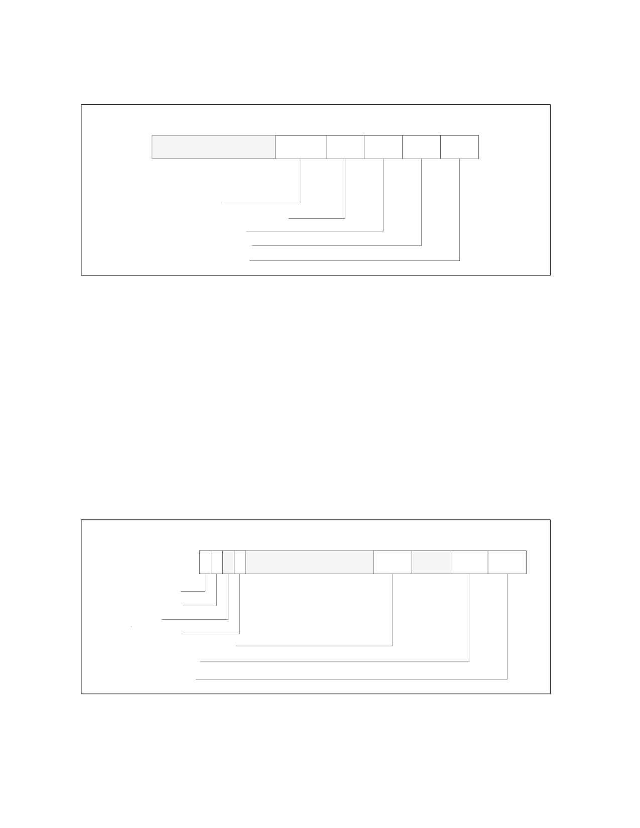
The structure of the IA32_HWP_REQUEST_PKG MSR (package-level) is identical to the IA32_HWP_REQUEST MSR
with the exception of the the Package Control bit field and the five valid bit fields, which do not exist in the
IA32_HWP_REQUEST_PKG MSR. Field values written to this MSR apply to all logical processors within the physical
package with the exception of logical processors whose IA32_HWP_REQUEST.Package Control field is clear (zero).
Single P-state Control mode is only supported when IA32_HWP_REQUEST_PKG is not supported.
15.4.4.3 IA32_HWP_PECI_REQUEST_INFO MSR (Address 775H Package Scope)
When an embedded system controller is integrated in the platform, it can override some of the OS HWP Request
settings via the PECI mechanism. PECI initiated settings take precedence over the relevant fields in the
IA32_HWP_REQUEST MSR and in the IA32_HWP_REQUEST_PKG MSR, irrespective of the Package Control bit or
the Valid Bit values described above. PECI can independently control each of: Minimum Performance, Maximum
Performance and EPP fields. This MSR contains both the PECI induced values and the control bits that indicate
whether the embedded controller actually set the processor to use the respective value.
PECI override is supported if CPUID[6].EAX[16] is set.
63 62 61 60 59
32 31
24 23
16 15
8 7
0
Reserved
Reserved
Min PECI Override
Max PECI Override
Reserved
EPP PECI Override
Energy_Performance_Preference
Maximum_Performance
Minimum_Performance
Figure 15-8. IA32_HWP_PECI_REQUEST_INFO MSR
Vol. 3B
15-11
POWER AND THERMAL MANAGEMENT
The layout of the IA32_HWP_PECI_REQUEST_INFO MSR is shown in Figure 15-8. This MSR is writable by the
embedded controller but is read-only by software executing on the CPU. This MSR has Package scope. The bit fields
are described below:
• Minimum_Performance (bits 7:0, RO) — Used by the OS to read the latest value of PECI minimum
performance input.
• Maximum_Performance (bits 15:8, RO) — Used by the OS to read the latest value of PECI maximum
performance input.
• Bits 23:16 are reserved and must be zero.
• Energy_Performance_Preference (bits 31:24, RO) — Used by the OS to read the latest value of PECI
energy performance preference input.
• Bits 59:32 are reserved and must be zero.
• EPP_PECI_Override (bit 60, RO) — Indicates whether PECI if currently overriding the Energy Performance
Preference input. If set(1), PECI is overriding the Energy Performance Preference input. If clear(0), OS has
control over Energy Performance Preference input.
• Bit 61 is reserved and must be zero.
• Max_PECI_Override (bit 62, RO) — Indicates whether PECI if currently overriding the Maximum
Performance input. If set(1), PECI is overriding the Maximum Performance input. If clear(0), OS has control
over Maximum Performance input.
• Min_PECI_Override (bit 63, RO) — Indicates whether PECI if currently overriding the Minimum Performance
input. If set(1), PECI is overriding the Minimum Performance input. If clear(0), OS has control over Minimum
Performance input.
HWP Request Field Hierarchical Resolution
HWP Request field resolution is fed by three MSRs: IA32_HWP_REQUEST, IA32_HWP_REQUEST_PKG, and
IA32_HWP_PECI_REQUEST_INFO. The flow that the processor goes through to resolve which field value is chosen
is shown below.
For each of the two HWP Request fields; Desired and Activity Window:
If IA32_HWP_REQUEST.PACKAGE_CONTROL = 1 and IA32_HWP_REQUEST.<field> valid bit = 0
Resolved Field Value = IA32_HWP_REQUEST_PKG.<field>
Else
Resolved Field Value = IA32_HWP_REQUEST.<field>
For each of the three HWP Request fields; Min, Max, and EPP:
If IA32_HWP_PECI_REQUEST_INFO.<field> PECI Override bit = 1
Resolved Field Value = IA32_HWP_PECI_REQUEST_INFO.<field>
Else if IA32_HWP_REQUEST.PACKAGE_CONTROL = 1 and IA32_HWP_REQUEST.<field> valid bit = 0
Resolved Field Value = IA32_HWP_REQUEST_PKG.<field>
Else
Resolved Field Value = IA32_HWP_REQUEST.<field>
15.4.4.4 IA32_HWP_CTL MSR (Address: 776H Logical Processor Scope)
IA32_HWP_CTL[0] controls the behavior of IA32_HWP_REQUEST Package Control [bit 42]. This control bit allows
the IA32_HWP_REQUEST MSR to stay in INIT mode most of the time (Control Bit is equal to its RESET value of 0)
thus avoiding actual saving/restoring of the MSR contents when the OS adds it to the register set saved and
restored by XSAVES/XRSTORS.
• When IA32_HWP_CTL[0] = 0:
— If IA32_HWP_REQUEST[42] = 0, the processor ignores all fields of the IA32_HWP_REQUEST_PKG MSR and
selects all HWP values (Min, Max, EPP, Desired, Activity Window) from the IA32_HWP_REQUEST MSR.
— If IA32_HWP_REQUEST[42] = 1, the processor selects the HWP values (Min, Max, EPP, Desired, Activity
Window) either from the IA32_HWP_REQUEST MSR or from the IA32_HWP_REQUEST_PKG MSR according
15-12
Vol. 3B

POWER AND THERMAL MANAGEMENT
to the values contained in the IA32_HWP_REQUEST MSR bit fields [bits 63:59]. See Section 15.4.4.1 for
additional details.
• When IA32_HWP_CTL[0] = 1, the behavior is reversed:
— If IA32_HWP_REQUEST[42] = 1, the processor ignores all fields of the IA32_HWP_REQUEST_PKG MSR and
selects all HWP values (Min, Max, EPP, Desired, Activity Window) from the IA32_HWP_REQUEST MSR.
— If IA32_HWP_REQUEST[42] = 0, the processor selects the HWP values (Min, Max, EPP, Desired, Activity
Window) either from the IA32_HWP_REQUEST MSR or from the IA32_HWP_REQUEST_PKG MSR according
to the values contained in the IA32_HWP_REQUEST MSR bit fields [bits 63:59]. See Section 15.4.4.1 for
additional details.
Section 15-2 summarizes the IA32_HWP_CTL MSR bit 0 control behavior.
Table 15-2. IA32_HWP_CTL MSR Bit 0 Behavior
Field
Description
Thread request
Defines which HWP Request MSR is used, whether thread level or package level. When the package MSR is used, the
PKG CTL
thread MSR valid bits define which thread MSR fields override the package (default 0).
meaning
IA32_HWP_CTL[PKG_CTL_PLR]
IA32_HWP_REQUEST[PKG_CTL]
HWP Request MSR Used
0
0
IA32_HWP_REQUEST MSR
0
1
IA32_HWP_REQUEST_PKG MSR
1
0
IA32_HWP_REQUEST_PKG MSR
1
1
IA32_HWP_REQUEST MSR
This MSR is supported if CPUID[6].EAX[22] is set.
If the IA32_PM_ENABLE[HWP_ENABLE] (bit 0 ) is not set, access to this MSR will generate a #GP fault.
15.4.5 HWP Feedback
The processor provides several types of feedback to the OS during HWP operation.
The IA32_MPERF MSR and IA32_APERF MSR mechanism (see Section 15.2) allows the OS to calculate the resultant
effective frequency delivered over a time period. Energy efficiency and performance optimizations directly impact
the resultant effective frequency delivered.
The layout of the IA32_HWP_STATUS MSR is shown in Figure 15-9. It provides feedback regarding changes to
IA32_HWP_CAPABILITIES.Guaranteed_Performance, IA32_HWP_CAPABILITIES.Highest_Performance, excur-
sions to IA32_HWP_CAPABILITIES.Minimum_Performance, and PECI_Override entry/exit events. The bit fields are
described below:
• Guaranteed_Performance_Change (bit 0, RWC0) — If set (1), a change to Guaranteed_Performance has
occurred. Software should query IA32_HWP_CAPABILITIES.Guaranteed_Performance value to ascertain the
new Guaranteed Performance value and to assess whether to re-adjust HWP hints via IA32_HWP_REQUEST.
Software must clear this bit by writing a zero (0).
• Bit 1 is reserved and must be zero.
• Excursion_To_Minimum (bit 2, RWC0) — If set (1), an excursion to Minimum_Performance of
IA32_HWP_REQUEST has occurred. Software must clear this bit by writing a zero (0).
• Highest_Change (bit 3, RWC0) — If set (1), a change to Highest Performance has occurred. Software
should query IA32_HWP_CAPABILITIES to ascertain the new Highest Performance value. Software must clear
this bit by writing a zero (0). Interrupts upon Highest Performance change are supported if CPUID[6].EAX[15]
is set.
• PECI_Override_Entry (bit 4, RWC0) — If set (1), an embedded/management controller has started a PECI
override of one or more OS control hints (Min, Max, EPP) specified in IA32_HWP_REQUEST or IA32_HWP_RE-
QUEST_PKG. Software may query IA32_HWP_PECI_REQUEST_INFO MSR to ascertain which fields are now
overridden via the PECI mechanism and what their values are (see Section 15.4.4.3 for additional details).
Vol. 3B
15-13

POWER AND THERMAL MANAGEMENT
Software must clear this bit by writing a zero (0). Interrupts upon PECI override entry are supported if
CPUID[6].EAX[16] is set.
• PECI_Override_Exit (bit 5, RWC0) — If set (1), an embedded/management controller has stopped
overriding one or more OS control hints (Min, Max, EPP) specified in IA32_HWP_REQUEST or IA32_HWP_RE-
QUEST_PKG. Software may query IA32_HWP_PECI_REQUEST_INFO MSR to ascertain which fields are still
overridden via the PECI mechanism and which fields are now back under software control (see Section 15.4.4.3
for additional details). Software must clear this bit by writing a zero (0). Interrupts upon PECI override exit are
supported if CPUID[6].EAX[16] is set.
• Bits 63:6 are reserved and must be zero.
63
6 5 4 3 2 1 0
Reserved
PECI_Override_Exit
PECI_Override_Entry
Highest_Change
Excursion_To_Minimum
Reserved
Guaranteed_Performance_Change
Figure 15-9. IA32_HWP_STATUS MSR
The status bits of IA32_HWP_STATUS must be cleared (0) by software so that a new status condition change will
cause the hardware to set the bit again and issue the notification. Status bits are not set for “normal” excursions,
e.g., running below Minimum Performance for short durations during C-state exit. Changes to Guaranteed_Perfor-
mance, Highest_Performance, excursions to Minimum_Performance, or PECI_Override entry/exit will occur no
more than once per second.
The OS can determine the specific reasons for a Guaranteed_Performance change or an excursion to Mini-
mum_Performance in IA32_HWP_REQUEST by examining the associated status and log bits reported in the
IA32_THERM_STATUS MSR. The layout of the IA32_HWP_STATUS MSR that HWP uses to support software query of
HWP feedback is shown in Figure 15-10. The bit fields of IA32_THERM_STATUS associated with HWP feedback are
described below (Bit fields of IA32_THERM_STATUS unrelated to HWP can be found in Section 15.8.5.2).
15-14
Vol. 3B

POWER AND THERMAL MANAGEMENT
63
32 31
27
23 22
16
15
14 1312
11
10
9
8
7
6
5
4
3
2
1
0
Reserved
Reading Valid
Resolution in Deg. Celsius
Digital Readout
Cross-domain Limit Log
Cross-domain Limit Status
Current Limit Log
Current Limit Status
Power Limit Notification Log
Power Limit Notification Status
Thermal Threshold #2 Log
Thermal Threshold #2 Status
Thermal Threshold #1 Log
Thermal Threshold #1 Status
Critical Temperature Log
Critical Temperature Status
PROCHOT# or FORCEPR# Log
PROCHOT# or FORCEPR# Event
Thermal Status Log
Thermal Status
Figure 15-10. IA32_THERM_STATUS Register With HWP Feedback
•
Bits 11:0, See Section 15.8.5.2.
•
Current Limit Status (bit 12, RO) — If set (1), indicates an electrical current limit (e.g., Electrical Design
Point/IccMax) is being exceeded and is adversely impacting energy efficiency optimizations.
•
Current Limit Log (bit 13, RWC0) — If set (1), an electrical current limit has been exceeded that has
adversely impacted energy efficiency optimizations since the last clearing of this bit or a reset. This bit is sticky,
software may clear this bit by writing a zero (0).
•
Cross-domain Limit Status (bit 14, RO) — If set (1), indicates another hardware domain (e.g., processor
graphics) is currently limiting energy efficiency optimizations in the processor core domain.
•
Cross-domain Limit Log (bit 15, RWC0) — If set (1), indicates another hardware domain (e.g., processor
graphics) has limited energy efficiency optimizations in the processor core domain since the last clearing of this
bit or a reset. This bit is sticky, software may clear this bit by writing a zero (0).
•
Bits 63:16, See Section 15.8.5.2.
15.4.5.1 Non-Architectural HWP Feedback
The Productive Performance (MSR_PPERF) MSR (non-architectural) provides hardware's view of workload scal-
ability, which is a rough assessment of the relationship between frequency and workload performance, to software.
The layout of the MSR_PPERF is shown in Figure 15-11.
63
0
PCNT - Productive Performance Count
Figure 15-11. MSR_PPERF MSR
• PCNT (bits 63:0, RO) — Similar to IA32_APERF but only counts cycles perceived by hardware as contributing
to instruction execution (e.g., unhalted and unstalled cycles). This counter increments at the same rate as
IA32_APERF, where the ratio of (ΔPCNT/ΔACNT) is an indicator of workload scalability (0% to 100%). Note that
values in this register are valid even when HWP is not enabled.
Vol. 3B
15-15

POWER AND THERMAL MANAGEMENT
15.4.6 HWP Notifications
Processors may support interrupt-based notification of changes to HWP status as indicated by CPUID. If supported,
the IA32_HWP_INTERRUPT MSR is used to enable interrupt-based notifications. Notification events, when enabled,
are delivered using the existing thermal LVT entry. The layout of the IA32_HWP_INTERRUPT is shown in
Figure 15-12. The bit fields are described below:
63
4 3 2 1 0
Reserved
EN_PECI_OVERRIDE
EN_Highest_Change
EN_Excursion_Minimum
EN_Guaranteed_Performance_Change
Figure 15-12. IA32_HWP_INTERRUPT MSR
• EN_Guaranteed_Performance_Change (bit 0, RW) — When set (1), an HWP Interrupt will be generated
whenever a change to the IA32_HWP_CAPABILITIES.Guaranteed_Performance occurs. The default value is 0
(Interrupt generation is disabled).
• EN_Excursion_Minimum (bit 1, RW) — When set (1), an HWP Interrupt will be generated whenever the
HWP hardware is unable to meet the IA32_HWP_REQUEST.Minimum_Performance setting. The default value is
0 (Interrupt generation is disabled).
• EN_Highest_Change (bit 2, RW) — When set (1), an HWP Interrupt will be generated whenever a change to
the IA32_HWP_CAPABILITIES.Highest_Performance occurs. The default value is 0 (interrupt generation is
disabled). Interrupts upon Highest Performance change are supported if CPUID[6].EAX[15] is set.
• EN_PECI_OVERRIDE (bit 3, RW) — When set (1), an HWP Interrupt will be generated whenever PECI starts
or stops overriding any of the three HWP fields described in Section 15.4.4.3. The default value is 0 (interrupt
generation is disabled). See Section 15.4.5 and Section 15.4.4.3 for details on how the OS learns what is the
current set of HWP fields that are overridden by PECI. Interrupts upon PECI override change are supported if
CPUID[6].EAX[16] is set.
• Bits 63:4 are reserved and must be zero.
15.4.7 Idle Logical Processor Impact on Core Frequency
Intel processors use one of two schemes for setting core frequency:
1. All cores share same frequency.
2. Each physical core is set to a frequency of its own.
In both cases the two logical processors that share a single physical core are set to the same frequency, so the
processor accounts for the IA32_HWP_REQUEST MSR fields of both logical processors when defining the core
frequency or the whole package frequency.
When CPUID[6].EAX[20] is set and only one logical processor of the two is active, while the other is idle (in any
C1 sub-state or in a deeper sleep state), only the active logical processor's IA32_HWP_REQUEST MSR fields
are considered, i.e., the HWP Request fields of a logical processor in the C1E sub-state or in a deeper sleep state
are ignored.
Note: when a logical processor is in C1 state its HWP Request fields are accounted for.
15-16
Vol. 3B

POWER AND THERMAL MANAGEMENT
15.4.8 Fast Write of Uncore MSR (Model Specific Feature)
There are a few logical processor scope MSRs whose values need to be observed outside the logical processor. The
WRMSR instruction takes over 1000 cycles to complete (retire) for those MSRs. This overhead forces operating
systems to avoid writing them too often whereas in many cases it is preferable that the OS writes them quite
frequently for optimal power/performance operation of the processor.
The model specific “Fast Write MSR” feature reduces this overhead by an order of magnitude to a level of 100 cycles
for a selected subset of MSRs.
Note: Writes to Fast Write MSRs are posted, i.e., when the WRMSR instruction completes, the data may still be “in
transit” within the processor. Software can check the status by querying the processor to ensure data is already
visible outside the logical processor (see Section 15.4.8.3 for additional details). Once the data is visible outside
the logical processor, software is ensured that later writes by the same logical processor to the same MSR will be
visible later (will not bypass the earlier writes).
MSRs that are selected for Fast Write are specified in a special capability MSR (see Section 15.4.8.1). Architectural
MSRs that existed prior to the introduction of this feature and are selected for Fast Write, thus turning from slow to
fast write MSRs, will be noted as such via a new CPUID bit. New MSRs that are fast upon introduction will be docu-
mented as such without an additional CPUID bit.
Three model specific MSRs are associated with the feature itself. They enable enumerating, controlling, and moni-
toring it. All three are logical processor scope.
15.4.8.1 FAST_UNCORE_MSRS_CAPABILITY (Address: 0x65F, Logical Processor Scope)
Operating systems or BIOS can read the FAST_UNCORE_MSRS_CAPABILITY MSR to enumerate those MSRs that
are Fast Write MSRs.
63
1 0
Reserved
FAST_IA32_HWP_REQUEST MSR
Figure 15-13. FAST_UNCORE_MSRS_CAPABILITY MSR
• FAST_IA32_HWP_REQUEST MSR (bit 0, RO) — When set (1), indicates that the IA32_HWP_REQUEST MSR
is supported as a Fast Write MSR. A value of 0 indicates the IA32_HWP_REQUEST MSR is not supported as a
Fast Write MSR.
• Bits 63:1 are reserved and must be zero.
15.4.8.2 FAST_UNCORE_MSRS_CTL (Address: 0x657, Logical Processor Scope)
Operating Systems or BIOS can use the FAST_UNCORE_MSRS_CTL MSR to opt-in or opt-out for fast write of
specific MSRs that are enabled for Fast Write by the processor.
Note: Not all MSRs that are selected for this feature will necessarily have this opt-in/opt-out option. They may be
supported in fast write mode only.
Vol. 3B
15-17

POWER AND THERMAL MANAGEMENT
63
1 0
Reserved
FAST_IA32_HWP_REQUEST_MSR_ENABLE
Figure 15-14. FAST_UNCORE_MSRS_CTL MSR
• FAST_IA32_HWP_REQUEST_MSR_ENABLE (bit 0, RW) — When set (1), enables fast access mode for the
IA32_HWP_REQUEST MSR and sets the low latency, posted IA32_HWP_REQUESRT MSR' CPUID[6].EAX[18].
The default value is 0. Note that this bit can only be enabled once from the default value. Once set, writes to
this bit are ignored. Only RESET will clear this bit.
• Bits 63:1 are reserved and must be zero.
15.4.8.3 FAST_UNCORE_MSRS_STATUS (Address: 0x65E, Logical Processor Scope)
Software that executes the WRMSR instruction of a Fast Write MSR can check whether the data is already visible
outside the logical processor by reading the FAST_UNCORE_MSRS_STATUS MSR. For each Fast Write MSR there is
a status bit that indicates whether the data is already visible outside the logical processor or is still in “transit”.
63
1 0
Reserved
FAST_IA32_HWP_REQUEST_WRITE_STATUS
Figure 15-15. FAST_UNCORE_MSRS_STATUS MSR
• FAST_IA32_HWP_REQUEST_WRITE_STATUS (bit 0, RO) — Indicates whether the CPU is still in the
middle of writing IA32_HWP_REQUEST MSR, even after the WRMSR instruction has retired. A value of 1
indicates the last write of IA32_HWP_REQUEST is still ongoing. A value of 0 indicates the last write of
IA32_HWP_REQUEST is visible outside the logical processor.
• Bits 63:1 are reserved and must be zero.
15.4.9 Fast_IA32_HWP_REQUEST CPUID
IA32_HWP_REQUEST is an architectural MSR that exists in processors whose CPUID[6].EAX[7] is set (HWP BASE
is enabled). This MSR has logical processor scope, but after its contents are written the contents become visible
outside the logical processor. When the FAST_IA32_HWP_REQUEST CPUID[6].EAX[18] bit is set, writes to the
IA32_HWP_REQUEST MSR are visible outside the logical processor via the “Fast Write” feature described in Section
15.4.8.
15.4.10 Recommendations for OS use of HWP Controls
Common Cases of Using HWP
The default HWP control field values are expected to be suitable for many applications. The OS can enable autono-
mous HWP for these common cases by
15-18
Vol. 3B
POWER AND THERMAL MANAGEMENT
• Setting IA32_HWP_REQUEST.Desired Performance = 0 (hardware autonomous selection determines the
performance target). Set IA32_HWP_REQUEST.Activity Window = 0 (enable HW dynamic selection of window
size).
To maximize HWP benefit for the common cases, the OS should set
• IA32_HWP_REQUEST.Minimum_Performance = IA32_HWP_CAPABILITIES.Lowest_Performance and
• IA32_HWP_REQUEST.Maximum_Performance = IA32_HWP_CAPABILITIES.Highest_Performance.
Setting IA32_HWP_REQUEST.Minimum_Performance = IA32_HWP_REQUEST.Maximum_Performance is function-
ally equivalent to using of the IA32_PERF_CTL interface and is therefore not recommended (bypassing HWP).
Calibrating HWP for Application-Specific HWP Optimization
In some applications, the OS may have Quality of Service requirements that may not be met by the default values.
The OS can characterize HWP by:
• keeping IA32_HWP_REQUEST.Minimum_Performance = IA32_HWP_REQUEST.Maximum_Performance to
prevent non-linearity in the characterization process,
• utilizing the range values enumerated from the IA32_HWP_CAPABILITIES MSR to program IA32_HWP_RE-
QUEST while executing workloads of interest and observing the power and performance result.
The power and performance result of characterization is also influenced by the IA32_HWP_REQUEST.Energy
Performance Preference field, which must also be characterized.
Characterization can be used to set IA32_HWP_REQUEST.Minimum_Performance to achieve the required QOS in
terms of performance. If IA32_HWP_REQUEST.Minimum_Performance is set higher than IA32_HWP_CAPABILI-
TIES.Guaranteed Performance then notification of excursions to Minimum Performance may be continuous.
If autonomous selection does not deliver the required workload performance, the OS should assess the current
delivered effective frequency and for the duration of the specific performance requirement set IA32_HWP_RE-
QUEST.Desired_Performance ≠ 0 and adjust IA32_HWP_REQUEST.Energy_Performance_Preference as necessary
to achieve the required workload performance. The MSR_PPERF.PCNT value can be used to better comprehend the
potential performance result from adjustments to IA32_HWP_REQUEST.Desired_Performance. The OS should set
IA32_HWP_REQUEST.Desired_Performance = 0 to re-enable autonomous selection.
Tuning for Maximum Performance or Lowest Power Consumption
Maximum performance will be delivered by setting IA32_HWP_REQUEST.Minimum_Performance = IA32_HWP_RE-
QUEST.Maximum_Performance = IA32_HWP_CAPABILITIES.Highest_Performance and setting IA32_HWP_RE-
QUEST.Energy_Performance_Preference = 0 (performance preference).
Lowest power will be achieved by setting IA32_HWP_REQUEST.Minimum_Performance = IA32_HWP_RE-
QUEST.Maximum_Performance = IA32_HWP_CAPABILITIES.Lowest_Performance and setting IA32_HWP_RE-
QUEST.Energy_Performance_Preference = 0FFH (energy efficiency preference).
Mixing Logical Processor and Package Level HWP Field Settings
Using the IA32_HWP_REQUEST Package_Control bit and the five valid bits in that MSR, the OS can mix and match
between selecting the Logical Processor scope fields and the Package level fields. For example, the OS can set all
logical cores' IA32_HWP_REQUEST.Package_Control bit to ‘1’, and for those logical processors if it prefers a
different EPP value than the one set in the IA32_HWP_REQUEST_PKG MSR, the OS can set the desired EPP value
and the EPP valid bit. This overrides the package EPP value for only a subset of the logical processors in the
package.
Additional Guidelines
Set IA32_HWP_REQUEST.Energy_Performance_Preference as appropriate for the platform's current mode of oper-
ation. For example, a mobile platforms' setting may be towards performance preference when on AC power and
more towards energy efficiency when on DC power.
The use of the Running Average Power Limit (RAPL) processor capability (see section 14.7.1) is highly recom-
mended when HWP is enabled. Use of IA32_HWP_Request.Maximum_Performance for thermal control is subject to
limitations and can adversely impact the performance of other processor components, e.g., graphics
Vol. 3B
15-19
POWER AND THERMAL MANAGEMENT
If default values deliver undesirable performance latency in response to events, the OS should set IA32_HWP_RE-
QUEST. Activity_Window to a low (non-zero) value and IA32_HWP_REQUEST.Energy_Performance_Preference
towards performance (0) for the event duration.
Similarly, for “real-time” threads, set IA32_HWP_REQUEST.Energy_Performance_Preference towards performance
(0) and IA32_HWP_REQUEST. Activity_Window to a low value, e.g., 01H, for the duration of their execution.
When executing low priority work that may otherwise cause the hardware to deliver high performance, set
IA32_HWP_REQUEST. Activity_Window to a longer value and reduce the IA32_HWP_Request.Maximum_Perfor-
mance value as appropriate to control energy efficiency. Adjustments to IA32_HWP_REQUEST.Energy_Perfor-
mance_Preference may also be necessary.
15.5
HARDWARE DUTY CYCLING (HDC)
Intel processors may contain support for Hardware Duty Cycling (HDC), which enables the processor to autono-
mously force its components inside the physical package into idle state. For example, the processor may selectively
force only the processor cores into an idle state.
HDC is disabled by default on processors that support it. System software can dynamically enable or disable HDC
to force one or more components into an idle state or wake up those components previously forced into an idle
state. Forced Idling (and waking up) of multiple components in a physical package can be done with one WRMSR to
a packaged-scope MSR from any logical processor within the same package.
HDC does not delay events such as timer expiration, but it may affect the latency of short (less than 1 msec) soft-
ware threads, e.g., if a thread is forced to idle state just before completion and entering a “natural idle”.
HDC forced idle operation can be thought of as operating at a lower effective frequency. The effective average
frequency computed by software will include the impact of HDC forced idle.
The primary use of HDC is enable system software to manage low active workloads to increase the package level
C6 residency. Additionally, HDC can lower the effective average frequency in case or power or thermal limitation.
When HDC forces a logical processor, a processor core or a physical package to enter an idle state, its C-State is set
to C3 or deeper. The deep “C-states” referred to in this section are processor-specific C-states.
15.5.1 Hardware Duty Cycling Programming Interfaces
The programming interfaces provided by HDC include the following:
• The CPUID instruction allows software to discover the presence of HDC support in an Intel processor. Specifi-
cally, execute CPUID instruction with EAX=06H as input, bit 13 of EAX indicates the processor’s support of the
following aspects of HDC.
— Availability of HDC baseline resource, CPUID.06H:EAX[bit 13]: If this bit is set, HDC provides the following
architectural MSRs: IA32_PKG_HDC_CTL, IA32_PM_CTL1, and the IA32_THREAD_STALL MSRs.
• Additionally, HDC may provide several non-architectural MSR.
15-20
Vol. 3B

POWER AND THERMAL MANAGEMENT
Table 15-3. Architectural and non-Architecture MSRs Related to HDC
Address
Architec
Register Name
Description
tural
DB0H
Y
IA32_PKG_HDC_CTL
Package Enable/Disable HDC.
DB1H
Y
IA32_PM_CTL1
Per-logical-processor select control to allow/block HDC forced idling.
DB2H
Y
IA32_THREAD_STALL
Accumulate stalled cycles on this logical processor due to HDC forced idling.
653H
N
MSR_CORE_HDC_RESIDENCY
Core level stalled cycle counter due to HDC forced idling on one or more
logical processor.
655H
N
MSR_PKG_HDC_SHALLOW_RE
Accumulate the cycles the package was in C21 state and at least one logical
SIDENCY
processor was in forced idle
656H
N
MSR_PKG_HDC_DEEP_RESIDE
Accumulate the cycles the package was in the software specified Cx1 state
NCY
and at least one logical processor was in forced idle. Cx is specified in
MSR_PKG_HDC_CONFIG_CTL.
652H
N
MSR_PKG_HDC_CONFIG_CTL
HDC configuration controls
NOTES:
1. The package “C-states” referred to in this section are processor-specific C-states.
15.5.2 Package level Enabling HDC
The layout of the IA32_PKG_HDC_CTL MSR is shown in Figure 15-16. IA32_PKG_HDC_CTL is a writable MSR from
any logical processor in a package. The bit fields are described below:
63
1
0
Reserved
Reserved
HDC_PKG_Enable
Figure 15-16. IA32_PKG_HDC_CTL MSR
• HDC_PKG_Enable (bit 0, R/W) — Software sets this bit to enable HDC operation by allowing the processor
to force to idle all “HDC-allowed” (see Figure 15.5.3) logical processors in the package. Clearing this bit
disables HDC operation in the package by waking up all the processor cores that were forced into idle by a
previous ‘0’-to-’1’ transition in IA32_PKG_HDC_CTL.HDC_PKG_Enable. This bit is writable only if
CPUID.06H:EAX[bit 13] = 1. Default = zero (0).
• Bits 63:1 are reserved and must be zero.
After processor support is determined via CPUID, system software can enable HDC operation by setting IA32_PK-
G_HDC_CTL.HDC_PKG_Enable to 1. At reset, IA32_PKG_HDC_CTL.HDC_PKG_Enable is cleared to 0. A '0'-to-'1'
transition in HDC_PKG_Enable allows the processor to force to idle all HDC-allowed (indicated by the non-zero
state of IA32_PM_CTL1[bit 0]) logical processors in the package. A ‘1’-to-’0’ transition wakes up those HDC force-
idled logical processors.
Software can enable or disable HDC using this package level control multiple times from any logical processor in
the package. Note the latency of writing a value to the package-visible IA32_PKG_HDC_CTL.HDC_PKG_Enable is
longer than the latency of a WRMSR operation to a Logical Processor MSR (as opposed to package level MSR) such
as: IA32_PM_CTL1 (described in Section 15.5.3). Propagation of the change in IA32_PKG_HDC_CTL.HDC_PK-
G_Enable and reaching all HDC idled logical processor to be woken up may take on the order of core C6 exit
latency.
Vol. 3B
15-21

POWER AND THERMAL MANAGEMENT
15.5.3 Logical-Processor Level HDC Control
The layout of the IA32_PM_CTL1 MSR is shown in Figure 15-17. Each logical processor in a package has its own
IA32_PM_CTL1 MSR. The bit fields are described below:
63
1
0
Reserved
HDC_Allow_Block
Reserved
Figure 15-17. IA32_PM_CTL1 MSR
• HDC_Allow_Block (bit 0, R/W) — Software sets this bit to allow this logical processors to honor the
package-level IA32_PKG_HDC_CTL.HDC_PKG_Enable control. Clearing this bit prevents this logical processor
from using the HDC. This bit is writable only if CPUID.06H:EAX[bit 13] = 1. Default = one (1).
• Bits 63:1 are reserved and must be zero.
Fine-grain OS control of HDC operation at the granularity of per-logical-processor is provided by IA32_PM_CTL1. At
RESET, all logical processors are allowed to participate in HDC operation such that OS can manage HDC using the
package-level IA32_PKG_HDC_CTL.
Writes to IA32_PM_CTL1 complete with the latency that is typical to WRMSR to a Logical Processor level MSR.
When the OS chooses to manage HDC operation at per-logical-processor granularity, it can write to IA32_PM_CTL1
on one or more logical processors as desired. Each write to IA32_PM_CTL1 must be done by code that executes on
the logical processor targeted to be allowed into or blocked from HDC operation.
Blocking one logical processor for HDC operation may have package level impact. For example, the processor may
decide to stop duty cycling of all other Logical Processors as well.
The propagation of IA32_PKG_HDC_CTL.HDC_PKG_Enable in a package takes longer than a WRMSR to IA32_P-
M_CTL1. The last completed write to IA32_PM_CTL1 on a logical processor will be honored when a ‘0’-to-’1’ transi-
tion of IA32_PKG_HDC_CTL.HDC_PKG_Enable arrives to a logical processor.
15.5.4 HDC Residency Counters
There is a collection of counters available for software to track various residency metrics related to HDC operation.
In general, HDC residency time is defined as the time in HDC forced idle state at the granularity of per-logical-
processor, per-core, or package. At the granularity of per-core/package-level HDC residency, at least one of the
logical processor in a core/package must be in the HDC forced idle state.
15.5.4.1 IA32_THREAD_STALL
Software can track per-logical-processor HDC residency using the architectural MSR IA32_THREAD_STALL.The
layout of the IA32_THREAD_STALL MSR is shown in Figure 15-18. Each logical processor in a package has its own
IA32_THREAD_STALL MSR. The bit fields are described below:
63
0
Stall_cycle_cnt
Figure 15-18. IA32_THREAD_STALL MSR
15-22
Vol. 3B

POWER AND THERMAL MANAGEMENT
• Stall_Cycle_Cnt (bits 63:0, R/O) — Stores accumulated HDC forced-idle cycle count of this processor core
since last RESET. This counter increments at the same rate of the TSC. The count is updated only after the
logical processor exits from the forced idled C-state. At each update, the number of cycles that the logical
processor was stalled due to forced-idle will be added to the counter. This counter is available only if
CPUID.06H:EAX[bit 13] = 1. Default = zero (0).
A value of zero in IA32_THREAD_STALL indicates either HDC is not supported or the logical processor never
serviced any forced HDC idle. A non-zero value in IA32_THREAD_STALL indicates the HDC forced-idle residency
times of the logical processor. It also indicates the forced-idle cycles due to HDC that could appear as C0 time to
traditional OS accounting mechanisms (e.g., time-stamping OS idle/exit events).
Software can read IA32_THREAD_STALL irrespective of the state of IA32_PKG_HDC_CTL and IA32_PM_CTL1, as
long as CPUID.06H:EAX[bit 13] = 1.
15.5.4.2 Non-Architectural HDC Residency Counters
Processors that support HDC operation may provide the following model-specific HDC residency counters.
MSR_CORE_HDC_RESIDENCY
Software can track per-core HDC residency using the counter MSR_CORE_HDC_RESIDENCY. This counter incre-
ments when the core is in C3 state or deeper (all logical processors in this core are idle due to either HDC or other
mechanisms) and at least one of the logical processors is in HDC forced idle state. The layout of the MSR_CORE_H-
DC_RESIDENCY is shown in Figure 15-19. Each processor core in a package has its own MSR_CORE_HDC_RESI-
DENCY MSR. The bit fields are described below:
63
0
Core_Cx_duty_cycle_cnt
Figure 15-19. MSR_CORE_HDC_RESIDENCY MSR
• Core_Cx_Duty_Cycle_Cnt (bits 63:0, R/O) — Stores accumulated HDC forced-idle cycle count of this
processor core since last RESET. This counter increments at the same rate of the TSC. The count is updated
only after core C-state exit from a forced idled C-state. At each update, the increment counts cycles when the
core is in a Cx state (all its logical processor are idle) and at least one logical processor in this core was forced
into idle state due to HDC. If CPUID.06H:EAX[bit 13] = 0, attempt to access this MSR will cause a #GP fault.
Default = zero (0).
A value of zero in MSR_CORE_HDC_RESIDENCY indicates either HDC is not supported or this processor core never
serviced any forced HDC idle.
MSR_PKG_HDC_SHALLOW_RESIDENCY
The counter MSR_PKG_HDC_SHALLOW_RESIDENCY allows software to track HDC residency time when the
package is in C2 state, all processor cores in the package are not active and at least one logical processor was
forced into idle state due to HDC. The layout of the MSR_PKG_HDC_SHALLOW_RESIDENCY is shown in
Figure 15-20. There is one MSR_PKG_HDC_SHALLOW_RESIDENCY per package. The bit fields are described
below:
63
0
Pkg_Duty_cycle_cnt
Figure 15-20. MSR_PKG_HDC_SHALLOW_RESIDENCY MSR
Vol. 3B
15-23

POWER AND THERMAL MANAGEMENT
• Pkg_Duty_Cycle_Cnt (bits 63:0, R/O) — Stores accumulated HDC forced-idle cycle count of this processor
core since last RESET. This counter increments at the same rate of the TSC. Package shallow residency may be
implementation specific. In the initial implementation, the threshold is package C2-state. The count is updated
only after package C2-state exit from a forced idled C-state. At each update, the increment counts cycles when
the package is in C2 state and at least one processor core in this package was forced into idle state due to HDC.
If CPUID.06H:EAX[bit 13] = 0, attempt to access this MSR may cause a #GP fault. Default = zero (0).
A value of zero in MSR_PKG_HDC_SHALLOW_RESIDENCY indicates either HDC is not supported or this processor
package never serviced any forced HDC idle.
MSR_PKG_HDC_DEEP_RESIDENCY
The counter MSR_PKG_HDC_DEEP_RESIDENCY allows software to track HDC residency time when the package is
in a software-specified package Cx state, all processor cores in the package are not active and at least one logical
processor was forced into idle state due to HDC. Selection of a specific package Cx state can be configured using
MSR_PKG_HDC_CONFIG. The layout of the MSR_PKG_HDC_DEEP_RESIDENCY is shown in Figure 15-21. There is
one MSR_PKG_HDC_DEEP_RESIDENCY per package. The bit fields are described below:
63
0
Pkg_Cx_duty_cycle_cnt
Figure 15-21. MSR_PKG_HDC_DEEP_RESIDENCY MSR
• Pkg_Cx_Duty_Cycle_Cnt (bits 63:0, R/O) — Stores accumulated HDC forced-idle cycle count of this
processor core since last RESET. This counter increments at the same rate of the TSC. The count is updated only
after package C-state exit from a forced idle state. At each update, the increment counts cycles when the
package is in the software-configured Cx state and at least one processor core in this package was forced into
idle state due to HDC. If CPUID.06H:EAX[bit 13] = 0, attempt to access this MSR may cause a #GP fault.
Default = zero (0).
A value of zero in MSR_PKG_HDC_SHALLOW_RESIDENCY indicates either HDC is not supported or this processor
package never serviced any forced HDC idle.
MSR_PKG_HDC_CONFIG
MSR_PKG_HDC_CONFIG allows software to configure the package Cx state that the counter MSR_PKG_HD-
C_DEEP_RESIDENCY monitors. The layout of the MSR_PKG_HDC_CONFIG is shown in Figure 15-22. There is one
MSR_PKG_HDC_CONFIG per package. The bit fields are described below:
63
2
0
Reserved
HDC_Cx_Monitor
Reserved
Figure 15-22. MSR_PKG_HDC_CONFIG MSR
• Pkg_Cx_Monitor (bits 2:0, R/W) — Selects which package C-state the MSR_HDC_DEEP_RESIDENCY
counter will monitor. The encoding of the HDC_Cx_Monitor field are: 0: no-counting; 1: count package C2 only,
2: count package C3 and deeper; 3: count package C6 and deeper; 4: count package C7 and deeper; other
encodings are reserved. If CPUID.06H:EAX[bit 13] = 0, attempt to access this MSR may cause a #GP fault.
Default = zero (0).
• Bits 63:3 are reserved and must be zero.
15-24
Vol. 3B
POWER AND THERMAL MANAGEMENT
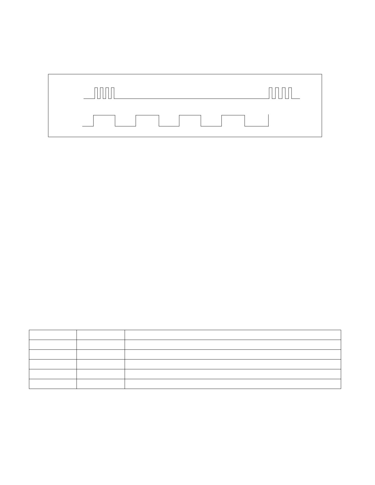
15.5.5 MPERF and APERF Counters Under HDC
HDC operation can be thought of as an average effective frequency drop due to all or some of the Logical Proces-
sors enter an idle state period.
1600 MHz: 25% Utilization /75% Forced Idle
Effective Frequency @ 100% Utilization: 400 MHz
Figure 15-23. Example of Effective Frequency Reduction and Forced Idle Period of HDC
By default, the IA32_MPERF counter counts during forced idle periods as if the logical processor was active. The
IA32_APERF counter does not count during forced idle state. This counting convention allows the OS to compute
the average effective frequency of the Logical Processor between the last MWAIT exit and the next MWAIT entry
(OS visible C0) by ΔACNT/ΔMCNT * TSC Frequency.
15.6
HARDWARE FEEDBACK INTERFACE AND INTEL® THREAD DIRECTOR
Intel processors that enumerate CPUID.06H.0H:EAX.HW_FEEDBACK[bit 19] as 1 support Hardware Feedback
Interface (HFI). Hardware provides guidance to the Operating System (OS) scheduler to perform optimal workload
scheduling through a hardware feedback interface structure in memory. Details on this table structure are
described in Section 15.6.1.
Intel processors that enumerate CPUID.06H.0H:EAX[bit 23] as 1 support Intel® Thread Director. Hardware
provides guidance to the Operating System (OS) scheduler to perform optimal workload scheduling through a
memory resident table and software thread specific index (Class ID) that points into that table and selects which
data to use for that software thread. Details on this table structure are described in Section 15.6.2.
15.6.1 Hardware Feedback Interface Table Structure
This structure has a global header that is 16 bytes in size. Following this global header, there is one 8 byte entry
per logical processor in the socket. The structure is designed as follows.
Table 15-4. Hardware Feedback Interface Structure
Byte Offset
Size (Bytes)
Description
0
16
Global Header
16
8
Per Logical Processor Entry
24
8
Per Logical Processor Entry
16 + n*8
8
Per Logical Processor Entry
Vol. 3B
15-25

POWER AND THERMAL MANAGEMENT
The global header is structured as shown in Table 15-5.
Table 15-5. Hardware Feedback Interface Global Header Structure
Byte Offset
Size (Bytes)
Field Name
Description
0
8
Timestamp
Timestamp of when the table was last updated by hardware. This is a
timestamp in crystal clock units.
Initialized by the OS to 0.
8
1
Performance
If bit 0 is set to 1, indicates the performance capability field for one or more
Capability Flags
logical processors was updated in the table and/or another bit in this field is
updated.
If bit 1 is set to 1, indicates a force idle/inject idle request to the OS for one
or more logical processors.
Initialized by the OS to 0.
9
1
Energy Efficiency
If bit 0 is set to 1, indicates the energy efficiency capability field for one or
Capability Changed
more logical processors was updated in the table and/or another bit in this
field is updated.
If bit 1 is set to 1, indicates a force idle/inject idle request to the OS for one
or more logical processors.
Initialized by the OS to 0.
10
6
Reserved
Initialized by the OS to 0.
The per logical processor scheduler feedback entry is structured as follows. The operating system can determine
the index of the logical processor feedback entry for a logical processor using CPUID.06H.0H:EDX[31:16] by
executing CPUID on that logical processor.
Table 15-6. Hardware Feedback Interface Logical Processor Entry Structure
Byte Offset
Size (Bytes)
Field Name
Description
0
1
Performance
Performance capability is an 8-bit value (0 ... 255) specifying the relative
Capability
performance level of a logical processor. Higher values indicate higher perfor-
mance; the lowest performance level of 0 indicates a recommendation to the OS to
not schedule any software threads on it for performance reasons. The OS
scheduler is expected to initialize the Hardware Feedback Interface Structure to 0
prior to enabling Hardware Feedback.
CPUID.06H.0H:EDX[0] enumerates support for Performance capability reporting.
1
1
Energy
Energy Efficiency capability is an 8-bit value (0 ... 255) specifying the relative
Efficiency
energy efficiency level of a logical processor. Higher values indicate higher energy
Capability
efficiency; the lowest energy efficiency capability of 0 indicates a recommendation
to the OS to not schedule any software threads on it for efficiency reasons. An
Energy Efficiency capability of 255 indicates which logical processors have the
highest relative energy efficiency capability. In addition, the value 255 is an
explicit recommendation for the OS to consolidate work on those logical
processors for energy efficiency reasons. The OS scheduler is expected to initialize
the Hardware Feedback Interface Structure to 0 prior to enabling Hardware
Feedback.
CPUID.06H.0H:EDX[1] enumerates support for Energy Efficiency capability
reporting.
2
6
Reserved
The OS scheduler is expected to initialize the Hardware Feedback Interface
Structure to 0 prior to enabling Hardware Feedback.
15-26
Vol. 3B

POWER AND THERMAL MANAGEMENT
15.6.2 Intel® Thread Director Table Structure
This structure has a global header that is at least 16 bytes in size. Its size depends on the number of classes and
capabilities enumerated by the CPUID instruction (see notes below Table 15-7). Following this global header there
are multiple Logical Processor related entries. The structure is designed as follows.
Table 15-7. Intel® Thread Director Table Structure
Byte Offset1,2,3
Size (Bytes)
Description
0
8 + CP4*CL4 + R85
Global Header
8 + CP*CL + R8
CL*CP + R8
Per Logical Processor Entry06
8 + 2*(CP*CL + R8)
CL*CP + R8
Per Logical Processor Entry1
8 + (N7 -1)*(CP*CL + R8)
CL*CP +R8
Logical Processor EntryN-1
NOTES:
1. Byte offset of Capabilitycp of Classcl change indication: 8 + CP * cl + cp.
2. Byte offset of LP Entryi : 8 + (i+1) * (CP * CL + R8).
3. Byte offset of capabilitycp of classcl of LP Entryi: 8 + (i+1) * (CP * CL + R8) + CP * cl + cp.
4. Both upper case CL and CP denote total number of classes and capabilities defined for the processor. Lower case cl and cp denote
one instance of a class or capability. cl and cp are counted starting at zero. See “CPUID—CPU Identification” in Chapter 3 of the Intel®
64 and IA-32 Architectures Software Developer’s Manual, Volume 2A for the number of classes (CL) and the number of supported
capabilities (CP). CP (# of capabilities): number of enumerated bits in CPUID.06H.0H.EDX[7:0] and CL (# of classes):
CPUID.06H.0H.ECX[15:8].
5. R8 is the number of bytes necessary to round up the Capability Change Indication array and the Logical Processor Entry to whole
multiple of 8 bytes.
6. Table size: 8 + (N+1)* (CP * CL + R8).
7. N is the number of Logical Processor Entries in the table. It is not greater than the number of Logical Processors on the socket, but
may be lower.
8. The Operating System can determine the index for the Logical Processor Entry within the Intel Thread Director table using
CPUID.06H.0H:EDX[31:16] by executing the CPUID instruction on that Logical Processor.
9. The Operating System should allocate space to accommodate for one such structure per socket in the system.
10. The Intel Thread Director table structure extends the Hardware Feedback Interface table structure without breaking backward
compatibility. The Hardware Feedback Interface can be viewed as having two capabilities and a single class.
The global header is structured as shown in Table 15-8.
Vol. 3B
15-27

POWER AND THERMAL MANAGEMENT
Table 15-8. Intel® Thread Director Global Header Structure
Size
Byte Offset
Description
(Bytes)
0
8
Time-stamp of when the table was last updated by hardware. This is a time-stamp in crystal clock units.
Initialized by the OS to 0.
8
1
Class 0 Performance
If bit 0 is set to 1, indicates the performance capability field for one or
Capability Flags
more logical processors was updated in the table and/or another bit in
this field is updated.
If bit 1 is set to 1, indicates a force idle/inject idle request to the OS for
one or more logical processors.
Initialized by the OS to 0.
8 + 1
1
Class 0 Energy Efficiency
If bit 0 is set to 1, indicates the energy efficiency capability field for
Capability Flags
one or more logical processors was updated in the table and/or
another bit in this field is updated.
If bit 1 is set to 1, indicates a force idle/inject idle request to the OS for
one or more logical processors.
Initialized by the OS to 0.
8 + CP - 1
1
Class 0 change indication for
Unavailable for capabilities that are not enumerated.
Capability #(CP-1) if exists
8 + CP
1
Class 1 Performance
If bit 0 is set to 1, indicates the performance capability field for one or
Capability Flags
more logical processors was updated in the table and/or another bit in
this field is updated.
If bit 1 is set to 1, indicates a force idle/inject idle request to the OS for
one or more logical processors.
Initialized by the OS to 0.
8 + CP + 1
1
Class 1 Energy Efficiency
If bit 0 is set to 1, indicates the energy efficiency capability field for
Capability Flags
one or more logical processors was updated in the table and/or
another bit in this field is updated.
If bit 1 is set to 1, indicates a force idle/inject idle request to the OS for
one or more logical processors.
Initialized by the OS to 0.
8 + 2*CP - 1
1
Class 1 change indication for
Unavailable for capabilities that are not enumerated.
Capability #(CP-1) if exists
Change indication for Capabilities of additional Classes if exist.
8 + (CL-1)*CP
1
Class #(CL-1) Performance
If bit 0 is set to 1, indicates the performance capability field for one or
Capability Flags
more logical processors was updated in the table and/or another bit in
this field is updated.
If bit 1 is set to 1, indicates a force idle/inject idle request to the OS for
one or more logical processors.
Initialized by the OS to 0.
8 + (CL-1)*CP + 1
1
Class #(CL-1) Energy
If bit 0 is set to 1, indicates the energy efficiency capability field for
Efficiency Capability Flags
one or more logical processors was updated in the table and/or
another bit in this field is updated.
If bit 1 is set to 1, indicates a force idle/inject idle request to the OS for
one or more logical processors.
Initialized by the OS to 0.
15-28
Vol. 3B

POWER AND THERMAL MANAGEMENT
Table 15-8. Intel® Thread Director Global Header Structure (Contd.)
Size
Byte Offset
Description
(Bytes)
8 + CL*CP - 1
1
Class #(CL-1) change
Unavailable for capabilities that are not enumerated.
indication for Capability #(CP-
1) if exists
8 + CL*CP
R8
Padding
Padding to nearest multiple of 8 bytes. Initialized by the OS to 0 prior
to enabling Intel Thread Director.
The logical processor capability entry in the Intel Thread Director table is structured as follows.
Table 15-9. Intel® Thread Director Logical Processor Entry Structure
Byte Offset
Size (Bytes)
Field Name
Description
0
1
Performance
Class 0 Performance capability is an 8-bit value (0 ... 255) specifying the relative
Capability
performance level of a single logical processor. Higher values indicate higher
performance; the lowest performance level of 0 indicates a recommendation to
the OS to not schedule any software threads on it for performance reasons.
Initialized by the OS to 0.
1
1
Energy
Class 0 Energy Efficiency capability is an 8-bit value (0 ... 255) specifying the
Efficiency
relative energy efficiency level of a logical processor. Higher values indicate higher
Capability
energy efficiency; the lowest energy efficiency capability of 0 indicates a recom-
mendation to the OS to not schedule any software threads on it for efficiency
reasons. An Energy Efficiency capability of 255 indicates which logical processors
have the highest relative energy efficiency capability. In addition, the value 255 is
an explicit recommendation for the OS to consolidate work on those logical
processors for energy efficiency reasons.
Initialized by the OS to 0.
CP - 1
1
Capability
Class 0 Capability #(CP-1) if exists. If the capability does not exist (is not
#(CP-1)
enumerated in the CPUID), the entry is unavailable (no space is reserved for future
use here).
CP
R8
Padding
Padding to nearest multiple of 8 bytes. Initialized by the OS to 0 prior to enabling
Intel Thread Director.
CP + R8
1
Performance
Class 1 Performance capability is an 8-bit value (0 ... 255) specifying the relative
Capability
performance level of a single logical processor. Higher values indicate higher
performance; the lowest performance level of 0 indicates a recommendation to
the OS to not schedule any software threads on it for performance reasons.
Initialized by the OS to 0.
CP + 1
1
Energy
Class 1 Energy Efficiency capability is an 8-bit value (0 ... 255) specifying the
Efficiency
relative energy efficiency level of a logical processor. Higher values indicate higher
Capability
energy efficiency; the lowest energy efficiency capability of 0 indicates a recom-
mendation to the OS to not schedule any software threads on it for efficiency
reasons. An Energy Efficiency capability of 255 indicates which logical processors
have the highest relative energy efficiency capability. In addition, the value 255 is
an explicit recommendation for the OS to consolidate work on those logical
processors for energy efficiency reasons.
Initialized by the OS to 0.
2*CP - 1
1
Capability
Class 1 Capability #(CP-1) if exists. If the capability does not exist (is not
#(CP-1)
enumerated in the CPUID), the entry is unavailable (no space is reserved for future
use here).
Vol. 3B
15-29

POWER AND THERMAL MANAGEMENT
Table 15-9. Intel® Thread Director Logical Processor Entry Structure (Contd.)
Byte Offset
Size (Bytes)
Field Name
Description
2*CP
R8
Padding
Padding to nearest multiple of 8 bytes. Initialized by the OS to 0 prior to enabling
Intel Thread Director.
(CL-1)*CP
1
Performance
Class #(CL-1) Performance capability is an 8-bit value (0 ... 255) specifying the
Capability
relative performance level of a single logical processor. Higher values indicate
higher performance; the lowest performance level of 0 indicates a recommen-
dation to the OS to not schedule any software threads on it for performance
reasons.
Initialized by the OS to 0.
(CL-1)*CP + 1
1
Energy
Class #(CL-1) Energy Efficiency capability is an 8-bit value (0 ... 255) specifying the
Efficiency
relative energy efficiency level of a logical processor. Higher values indicate higher
Capability
energy efficiency; the lowest energy efficiency capability of 0 indicates a recom-
mendation to the OS to not schedule any software threads on it for efficiency
reasons. An Energy Efficiency capability of 255 indicates which logical processors
have the highest relative energy efficiency capability. In addition, the value 255 is
an explicit recommendation for the OS to consolidate work on those logical
processors for energy efficiency reasons.
Initialized by the OS to 0.
CL*CP - 1
1
Capability
Class #(CL-1) Capability #(CP-1) if exists. If the capability does not exist (is not
#(CP-1)
enumerated in the CPUID), the entry is unavailable (no space is reserved for future
use here).
CL*CP
R8
Padding
Padding to nearest multiple of 8 bytes. Initialized by the OS to 0 prior to enabling
Intel Thread Director.
15.6.3 Intel® Thread Director Usage Model
When the OS Scheduler needs to decide which one of multiple free logical processors to assign to a software
thread that is ready to execute, it can choose one of the following options:
1. The free logical processor with the highest performance value of that software thread class, if the system is
scheduling for performance.
2. The free logical processor with the highest energy efficiency value of that software thread class, if the system
is scheduling for energy efficiency.
When the OS Scheduler needs to decide which of two logical processors (i,j) to assign to which of two software
threads whose Class IDs are k1 and k2, it can compute the two performance ratios: Perf Ratio1 = Perfik1 / Perfjk1
and Perf Ratio2 = Perfik2 / Perfjk2, or two energy efficiency ratios: Energy Eff. Ratio1 = Energy Effik1 / Energy Effjk1
and Energy Eff. Ratio2 = Energy Effik2 / Energy Effjk2 between the two logical processors for each of the two classes,
depending on whether the OS is scheduling for performance or for energy efficiency.
For example, assume that the system is scheduling for performance and that Perf Ratio1 > Perf Ratio2. The OS
Scheduler will assign the software thread whose Class ID is k1 to logical processor i, and the one whose Class ID is
k2 to logical processor j.
When the two software threads in question belong to the same Class ID, the OS Scheduler can schedule to higher
performance logical processors within that class when scheduling for performance and to higher energy efficiency
logical processors within that class when scheduling for energy efficiency.
The highest to lowest ordering may be different between classes across cores and between the performance
column and the energy efficiency column of the same class across cores.
15-30
Vol. 3B

POWER AND THERMAL MANAGEMENT
15.6.4 Hardware Feedback Interface Pointer
The physical address of the HFI/Intel Thread Director structure is programmed by the OS into a package scoped
MSR named IA32_HW_FEEDBACK_PTR. The MSR is structured as follows:
• Bits 63:MAXPHYADDR1 - Reserved.
• Bits MAXPHYADDR-1:12 - ADDR. This is the physical address of the page frame of the first page of this
structure.
• Bits 11:1 - Reserved.
• Bit 0 - Valid. When set to 1, indicates a valid pointer is programmed into the ADDR field of the MSR.
The address of this MSR is 17D0H. This MSR is cleared on processor reset to its default value of 0. It retains its
value upon INIT.
CPUID.06H.0H:EDX[11:8] enumerates the size of memory that must be allocated by the OS for this structure.
15.6.5 Hardware Feedback Interface Configuration
The operating system enables HFI/Intel Thread Director using a package scoped MSR named IA32_HW_FEED-
BACK_CONFIG (address 17D1H). This MSR is cleared on processor reset to its default value of 0. It retains its value
upon INIT.
The MSR is structured as follows:
• Bits 63:2 - Reserved.
• Bit 1 - Enable Intel Thread Director (or multi-class support). Both bits 0 and 1 must be set for Intel Thread
Director to be enabled. The extra class columns in the Intel Thread Director table are updated by hardware
immediately following setting those two bits, as well as during run time as necessary.
• Bit 0 - Enable. When set to 1, enables HFI.
Before enabling HFI, the OS must set a valid hardware feedback interface structure using IA32_HW_FEED-
BACK_PTR.
When the OS sets bit 0 only, the hardware populates class 0 capabilities only in the HFI structure. When bit 1 is set
after or together with bit 0, the Intel Thread Director multi-class structure is populated.
When either the HFI structure or the Intel Thread Director structure are ready to use by the OS, the hardware sets
IA32_PACKAGE_THERM_STATUS[bit 26]. An interrupt is generated by the hardware if IA32_PACKAGE_THERM_IN-
TERRUPT[bit 25] is set.
When the OS clears bit 1 but leaves bit 0 set, Intel Thread Director is disabled, but HFI is kept operational.
IA32_PACKAGE_THERM_STATUS[bit 26] is NOT set in this case.
Clearing bit 0 disables both HFI and Intel Thread Director, independent of the bit 1 state. Setting bit 1 to '1' while
keeping bit 0 at '0' is an invalid combination which is quietly ignored.
When the OS clears bit 0, hardware sets the IA32_PACKAGE_THERM_STATUS[bit 26] to 1 to acknowledge
disabling of the interface. The OS should wait for this bit to be set to 1 to reclaim the memory of the Intel Thread
Director structure, as by setting IA32_PACKAGE_THERM_STATUS[bit 26] hardware guarantees not to write into
the Intel Thread Director structure anymore.
The OS may clear bit 0 only after receiving an indication from the hardware that the structure initialization is
complete via the same IA32_PACKAGE_THERM_STATUS[bit 26], following enabling of HFI/Intel Thread Director,
thus avoiding a race condition between OS and hardware.
Bit 1 is valid only if CPUID[6].EAX[bit 23] is set. When setting this bit while support is not enumerated, the hard-
ware generates #GP.
Table 15-10 summarizes the control options described above.
See Section 15.6.9 for details on scenarios where IA32_HW_FEEDBACK_CONFIG bits are implicitly reset by the
hardware.
1. MAXPHYADDR is reported in CPUID.80000008H:EAX[7:0].
Vol. 3B
15-31

POWER AND THERMAL MANAGEMENT
Table 15-10. IA32_HW_FEEDBACK_CONFIG Control Options
Pre-Bit 1
Pre-Bit 0
Post-Bit 1
Post-Bit 0
Action
IA32_PACKAGE_THERM_STATUS [bit 26] and
Interrupt
0
0
0
0
Reset value.
Both Hardware Feedback Interface and Intel
Thread Director are disabled, no status bit set, no
interrupt is generated.
0
0
0
1
Enable HFI structure.
Set the status bit and generate interrupt if
enabled.
0
0
1
0
Invalid option; quietly
No action (no update in the table).
ignored by the hardware.
0
0
1
1
Enable HFI and Intel
Set the status bit and generate interrupt if
Thread Director.
enabled.
0
1
0
0
Disable HFI support.
Set the status bit and generate interrupt if
enabled.
0
1
1
0
Disable HFI and Intel
Set the status bit and generate interrupt if
Thread Director.
enabled.
0
1
1
1
Enable Intel Thread
Set the status bit and generate interrupt if
Director.
enabled.
1
0
0
0
No action; keeps HFI and
No action (no update in the table).
Intel Thread Director
disabled.
1
0
0
1
Enable HFI.
Set the status bit and generate interrupt if
enabled.
1
0
1
1
Enable HFI and Intel
Set the status bit and generate interrupt if
Thread Director.
enabled.
1
1
0
0
Disable HFI and Intel
Set the status bit and generate interrupt if
Thread Director.
enabled.
1
1
0
1
Disable Intel Thread
No action (no update in the table).
Director; keep HFI
enabled.
1
1
1
0
Disable HFI and Intel
Set the status bit and generate interrupt if
Thread Director.
enabled.
15.6.6 Hardware Feedback Interface Notifications
The IA32_PACKAGE_THERM_STATUS MSR is extended with a new bit, hardware feedback interface structure
change status (bit 26, R/WC0), to indicate that the hardware has updated the HFI/Intel Thread Director structure.
This is a sticky bit and once set, indicates that the OS should read the structure to determine the change and adjust
its scheduling decisions. Once set, the hardware will not generate any further updates to this structure until the OS
clears this bit by writing 0.
The OS can enable interrupt-based notifications when the structure is updated by hardware through a new enable
bit, hardware feedback interrupt enable (bit 25, R/W), in the IA32_PACKAGE_THERM_INTERRUPT MSR. When this
bit is set to 1, it enables the generation of an interrupt when the HFI/Intel Thread Director structure is updated by
hardware. When the enable bit transitions from 0 to 1, hardware will generate an initial notify, with the IA32_PACK-
AGE_THERM_STATUS bit 26 set to 1, to indicate that the OS should read the current HFI/Intel Thread Director
structure.
15-32
Vol. 3B
POWER AND THERMAL MANAGEMENT
15.6.7 Hardware Feedback Interface and Intel® Thread Director Structure Dynamic Update
The HFI/Intel Thread Director structure can be updated dynamically during run time. Changes to the structure may
occur to one or more of its cells. Such changes may occur for one or more logical processors. The hardware sets a
non-zero value in the “capability change” field of the HFI/Intel Thread Director structure as an indication for the OS
to read that capability for all logical processors. A thermal interrupt is delivered to indicate to the OS that the struc-
ture has just changed. Section 15.6.6 contains more details on this notification mechanism. The hardware clears
all “capability change” fields after the OS resets IA32_PACKAGE_THERM_STATUS[bit 26].
Zeroing a performance or energy efficiency cell hints to the OS that it is beneficial not to schedule software threads
of that class on the associated logical processor for performance or energy efficiency reasons, respectively. If SMT
is supported, it may be the case that the hardware zeroes one of the core's logical processors only. Zeroing the
performance and energy efficiency cells of all classes for a logical processor implies that the hardware provides a
hint to the OS to completely avoid scheduling work on that logical processor.
Zeroing a performance and energy efficiency cell hint of a logical processor across all classes along with Capability
Flag bit 1 set to 1 across all capabilities and classes, indicates to the OS to force idle logical processor(s), and if
affinitized activity occurs on those logical processor(s), the OS should inject idle periods such that overall utilization
of those idled cores has a minimal-to-no impact to power. Capability Flag bit 1 will be set to 1 while this hint
persists.
When EE=255 is set on one or more logical processors, it represents a request that the OS attempt to consolidate
work to those logical processors with EE=255. These requests are made when the SOC has knowledge that consol-
idating the work to a subset of cores will result in significantly better platform energy efficiency. Examples of
consolidating work would include, but not limited to, delaying less important work as needed to provide compute
bandwidth for more important work, and routing interrupts to the logical processors with EE=255. When the cumu-
lative workload requires performance greater than that which is available on the subset of cores with EE=255, it is
expected that the OS will scale the work out to additional logical processors.
A few example reasons for runtime changes in the HGS/Intel Thread Director Table:
• Over clocking run time update that changes the capability values.
• Change in run time physical constraints.
• Run time performance or energy efficiency optimization.
• Change in core frequency, voltage, or power budget.
15.6.8 Logical Processor Scope Intel® Thread Director Configuration
The operating system enables Intel Thread Director at the logical processor scope using a logical processor scope
MSR named IA32_HW_FEEDBACK_THREAD_CONFIG (address 17D4H).
The MSR is read/write and is structured as follows:
• Bits 63:1 - Reserved.
• Bit 0 - Enables Intel Thread Director. When set to 1, logical processor scope Intel Thread Director is enabled.
Default is 0 (disabled).
Bit 0 of the logical processor scope configuration MSR can be cleared or set regardless of the state of the
HFI/Intel Thread Director package configuration MSR state. Even when bit 0 of all logical processor configuration
MSRs is clear, the processor can still update the Intel Thread Director structure if it is still enabled in the
IA32_HW_FEEDBACK_CONFIG package scope MSR. When the operating system clears
IA32_HW_FEEDBACK_THREAD_CONFIG[bit 0], hardware clears the history accumulated on that logical processor
which otherwise drives assigning the Class ID to the software thread that executes on that logical processor. As
long as IA32_HW_FEEDBACK_THREAD_CONFIG[bit 0] is set, the Class ID is available for the operating system to
read, independent of the state of the package scope IA32_HW_FEEDBACK_CONFIG[1:0] bits.
See Section 15.6.9 for details on scenarios where IA32_HW_FEEDBACK_CONFIG bits are implicitly reset by the
hardware.
Vol. 3B
15-33
POWER AND THERMAL MANAGEMENT
15.6.9 Implicit Reset of Package and Logical Processor Scope Configuration MSRs
HFI/Intel Thread Director enable bits are reset by hardware in the following scenarios:
1. When GETSEC[SENTER] is executed:
a. The processor implicitly resets the HFI/Intel Thread Director enable bits in the IA32_HW_FEEDBACK_-
CONFIG MSR on all sockets (packages) in the system.
b. The processor implicitly resets the Intel Thread Director enable bit in the IA32_HW_FEEDBACK_THREAD_-
CONFIG MSR on all logical processors in the system across all sockets.
c. The processor implicitly clears the HFI/Intel Thread Director table structure pointer in the IA32_HW_FEED-
BACK_PTR package MSR across all sockets.
2. When GETSEC[ENTERACCS] is executed:
a. The processor implicitly resets the HFI/Intel Thread Director enable bits in the IA32_HW_FEEDBACK_-
CONFIG MSR on the socket where the GETSEC[ENTERACCS] instruction was executed.
b. The processor implicitly resets the Intel Thread Director enable bit in the IA32_HW_FEEDBACK_THREAD_-
CONFIG MSR on all logical processors on the socket where the GETSEC[ENTERACCS] instruction was
executed.
c. The processor implicitly clears the HFI/Intel Thread Director table structure pointer in the IA32_HW_FEED-
BACK_PTR package MSR on the socket where the GETSEC[ENTERACCS] instruction was executed.
3. When an INIT or a wait-for-SIPI state are processed by a logical processor:
a. The processor implicitly resets the Intel Thread Director enable bit in the IA32_HW_FEEDBACK_THREAD_-
CONFIG MSR on that logical processor, whether the signal was in the context of GETSEC[ENTERACCS] or
not.
If the OS requires HFI/Intel Thread Director to be active after exiting the measured environment or when
processing a SIPI event, it should re-enable HFI/Intel Thread Director.
15.6.10 Logical Processor Scope Intel® Thread Director Run Time Characteristics
The processor provides the operating system with run time feedback about the execution characteristics of the
software thread executing on logical processors whose IA32_HW_FEEDBACK_THREAD_CONFIG[bit 0] is set.
The run time feedback is communicated via a read-only MSR named IA32_THREAD_FEEDBACK_CHAR. This is a
logical processor scope MSR whose address is 17D2H. This MSR is structured as follows:
• Bit 63 - Valid bit. When set to 1 the OS Scheduler can use the Class ID (in bits 7:0) for its scheduling decisions.
If this bit is 0, the Class ID field should be ignored. It is recommended that the OS uses the last known Class ID
of the software thread for its scheduling decisions.
• Bits 62:8 - Reserved.
• Bits 7:0 - Application Class ID, pointing into the Intel Thread Director structure described in Table 15-8.
This MSR is valid only if CPUID.06H:EAX[bit 23] is set.
The valid bit is cleared by the hardware in the following cases:
• The hardware does not have enough information to provide the operating system with a reliable Class ID.
• The operating system cleared the logical processor’s IA32_HW_FEEDBACK_THREAD_CONFIG[bit 0] bit.
The HRESET instruction is executed while configured to reset the Intel Thread Director history.
15.6.11 Logical Processor Scope History
The operating system can reset the Intel Thread Director related history accumulated on the current logical pro-
cessor it is executing on by issuing the HRESET instruction. See “CPUID—CPU Identification” in Chapter 3 of the
Intel® 64 and IA-32 Architectures Software Developer’s Manual, Volume 2A, for enumeration of the HRESET
15-34
Vol. 3B

POWER AND THERMAL MANAGEMENT
instruction. See also the “HRESET—History Reset” instruction description in Chapter 3 of the Intel® 64 and IA-32
Architectures Software Developer’s Manual, Volume 2A.
15.6.11.1 Enabling Intel® Thread Director History Reset
The IA32_HRESET_ENABLE MSR is a read/write MSR and is structured as follows:
• Bits 63:32 - Reserved.
• Bits 31:1 - Reserved for other capabilities that can be reset by the HRESET instruction.
• Bit 0 - Enable reset of the Intel Thread Director history.
The operating system should set IA32_HRESET_ENABLE[bit 0] to enable Intel Thread Director history reset via
the HRESET instruction.
15.6.11.2 Implicit Intel® Thread Director History Reset
The Intel Thread Director history is implicitly reset in the following scenarios:
1. When the processor enters or exits SMM mode and IA32_DEBUGCTL MSR.FREEZE_WHILE_SMM (bit 14) is set,
the Intel Thread Director history is implicitly reset by the processor.
2. When GETSEC[SENTER] is executed, the processor resets the Intel Thread Director history on all logical
processors in the system, including logical processors on other sockets (other than the one GETSEC[SENTER]
is executed).
3. When GETSEC[ENTERACCS] is executed, the processor resets the Intel Thread Director history on the logical
processor it is executed on.
4. When an INIT or a wait-for-SIPI state are processed by a logical processor, the Intel Thread Director history is
reset whether the signal was a result of GETSEC[ENTERACCS] or not.
If the operating system requires HFI/Intel Thread Director to be active after exiting the measured environment or
when processing a SIPI event, it should re-enable HFI/Intel Thread Director.
15.7
MWAIT EXTENSIONS FOR ADVANCED POWER MANAGEMENT
IA-32 processors may support a number of C-states1 that reduce power consumption for inactive states. Intel Core
Solo and Intel Core Duo processors support both deeper C-state and MWAIT extensions that can be used by OS to
implement power management policy.
Software should use CPUID to discover if a target processor supports the enumeration of MWAIT extensions. If
CPUID.05H.ECX[Bit 0] = 1, the target processor supports MWAIT extensions and their enumeration (see Chapter
4, “Instruction Set Reference, M-U,” of Intel® 64 and IA-32 Architectures Software Developer’s Manual, Volume
2B).
If CPUID.05H.ECX[Bit 1] = 1, the target processor supports using interrupts as break-events for MWAIT, even
when interrupts are disabled. Use this feature to measure C-state residency as follows:
• Software can write to bit 0 in the MWAIT Extensions register (ECX) when issuing an MWAIT to enter into a
processor-specific C-state or sub C-state.
• When a processor comes out of an inactive C-state or sub C-state, software can read a timestamp before an
interrupt service routine (ISR) is potentially executed.
CPUID.05H.EDX allows software to enumerate processor-specific C-states and sub C-states available for use with
MWAIT extensions. IA-32 processors may support more than one C-state of a given C-state type. These are called
sub C-states. Numerically higher C-state have higher power savings and latency (upon entering and exiting) than
lower-numbered C-state.
1. The processor-specific C-states defined in MWAIT extensions can map to ACPI defined C-state types (C0, C1, C2, C3). The mapping
relationship depends on the definition of a C-state by processor implementation and is exposed to OSPM by the BIOS using the ACPI
defined _CST table.
Vol. 3B
15-35

POWER AND THERMAL MANAGEMENT
At CPL = 0, system software can specify desired C-state and sub C-state by using the MWAIT hints register (EAX).
Processors will not go to C-state and sub C-state deeper than what is specified by the hint register. If CPL > 0 and
if MONITOR/MWAIT is supported at CPL > 0, the processor will only enter C1-state (regardless of the C-state
request in the hints register).
Executing MWAIT generates an exception on processors operating at a privilege level where MONITOR/MWAIT are
not supported.
NOTE
If MWAIT is used to enter a C-state (including sub C-state) that is numerically higher than C1, a
store to the address range armed by MONITOR instruction will cause the processor to exit MWAIT if
the store was originated by other processor agents. A store from non-processor agent may not
cause the processor to exit MWAIT.
15.8
THERMAL MONITORING AND PROTECTION
The IA-32 architecture provides the following mechanisms for monitoring temperature and controlling thermal
power:
1. The catastrophic shutdown detector forces processor execution to stop if the processor’s core temperature
rises above a preset limit.
2. Automatic and adaptive thermal monitoring mechanisms force the processor to reduce it’s power
consumption in order to operate within predetermined temperature limits.
3. The software controlled clock modulation mechanism permits operating systems to implement power
management policies that reduce power consumption; this is in addition to the reduction offered by automatic
thermal monitoring mechanisms.
4. On-die digital thermal sensor and interrupt mechanisms permit the OS to manage thermal conditions
natively without relying on BIOS or other system board components.
The first mechanism is not visible to software. The other three mechanisms are visible to software using processor
feature information returned by executing CPUID with EAX = 1.
The second mechanism includes:
• Automatic thermal monitoring provides two modes of operation. One mode modulates the clock duty cycle;
the second mode changes the processor’s frequency. Both modes are used to control the core temperature of
the processor.
• Adaptive thermal monitoring can provide flexible thermal management on processors made of multiple
cores.
The third mechanism modulates the clock duty cycle of the processor. As shown in Figure 15-24, the phrase ‘duty
cycle’ does not refer to the actual duty cycle of the clock signal. Instead it refers to the time period during which the
clock signal is allowed to drive the processor chip. By using the stop clock mechanism to control how often the
processor is clocked, processor power consumption can be modulated.
Clock Applied to Processor
Stop-Clock Duty Cycle
25% Duty Cycle (example only)
Figure 15-24. Processor Modulation Through Stop-Clock Mechanism
15-36
Vol. 3B
POWER AND THERMAL MANAGEMENT
For previous automatic thermal monitoring mechanisms, software controlled mechanisms that changed processor
operating parameters to impact changes in thermal conditions. Software did not have native access to the native
thermal condition of the processor; nor could software alter the trigger condition that initiated software program
control.
The fourth mechanism (listed above) provides access to an on-die digital thermal sensor using a model-specific
register and uses an interrupt mechanism to alert software to initiate digital thermal monitoring.
15.8.1 Catastrophic Shutdown Detector
P6 family processors introduced a thermal sensor that acts as a catastrophic shutdown detector. This catastrophic
shutdown detector was also implemented in Pentium 4, Intel Xeon and Pentium M processors. It is always enabled.
When processor core temperature reaches a factory preset level, the sensor trips and processor execution is halted
until after the next reset cycle.
15.8.2 Thermal Monitor
Pentium 4, Intel Xeon and Pentium M processors introduced a second temperature sensor that is factory-calibrated
to trip when the processor’s core temperature crosses a level corresponding to the recommended thermal design
envelop. The trip-temperature of the second sensor is calibrated below the temperature assigned to the cata-
strophic shutdown detector.
15.8.2.1 Thermal Monitor 1
The Pentium 4 processor uses the second temperature sensor in conjunction with a mechanism called Thermal
Monitor 1 (TM1) to control the core temperature of the processor. TM1 controls the processor’s temperature by
modulating the duty cycle of the processor clock. Modulation of duty cycles is processor model specific. Note that
the processors STPCLK# pin is not used here; the stop-clock circuitry is controlled internally.
Support for TM1 is indicated by CPUID.1:EDX.TM[bit 29] = 1.
TM1 is enabled by setting the thermal-monitor enable flag (bit 3) in IA32_MISC_ENABLE; see Chapter 2, “Model-
Specific Registers (MSRs)‚” in the Intel® 64 and IA-32 Architectures Software Developer’s Manual, Volume 4.
Following a power-up or reset, the flag is cleared, disabling TM1. BIOS is required to enable only one automatic
thermal monitoring modes. Operating systems and applications must not disable the operation of these mecha-
nisms.
15.8.2.2 Thermal Monitor 2
An additional automatic thermal protection mechanism, called Thermal Monitor 2 (TM2), was introduced in the
Intel Pentium M processor and also incorporated in newer models of the Pentium 4 processor family. Intel Core Duo
and Solo processors, and Intel Core 2 Duo processor family all support TM1 and TM2. TM2 controls the core
temperature of the processor by reducing the operating frequency and voltage of the processor and offers a higher
performance level for a given level of power reduction than TM1.
TM2 is triggered by the same temperature sensor as TM1. The mechanism to enable TM2 may be implemented
differently across various IA-32 processor families with different CPUID signatures in the family encoding value,
but will be uniform within an IA-32 processor family.
Support for TM2 is indicated by CPUID.1:ECX.TM2[bit 8] = 1.
15.8.2.3 Two Methods for Enabling TM2
On processors with CPUID family/model/stepping signature encoded as 0x69n or 0x6Dn (early Pentium M proces-
sors), TM2 is enabled if the TM_SELECT flag (bit 16) of the MSR_THERM2_CTL register is set to 1 (Figure 15-25)
and bit 3 of the IA32_MISC_ENABLE register is set to 1.
Vol. 3B
15-37

POWER AND THERMAL MANAGEMENT
Following a power-up or reset, the TM_SELECT flag may be cleared. BIOS is required to enable either TM1 or TM2.
Operating systems and applications must not disable mechanisms that enable TM1 or TM2. If bit 3 of the IA32_-
MISC_ENABLE register is set and TM_SELECT flag of the MSR_THERM2_CTL register is cleared, TM1 is enabled.
31
16
0
Reserved
Reserved
TM_SELECT
Figure 15-25. MSR_THERM2_CTL Register On Processors with CPUID Family/Model/Stepping Signature Encoded
as 0x69n or 0x6Dn
On processors introduced after the Pentium 4 processor (this includes most Pentium M processors), the method
used to enable TM2 is different. TM2 is enable by setting bit 13 of IA32_MISC_ENABLE register to 1. This applies to
Intel Core Duo, Core Solo, and Intel Core 2 processor family.
The target operating frequency and voltage for the TM2 transition after TM2 is triggered is specified by the value
written to MSR_THERM2_CTL, bits 15:0 (Figure 15-26). Following a power-up or reset, BIOS is required to enable
at least one of these two thermal monitoring mechanisms. If both TM1 and TM2 are supported, BIOS may choose
to enable TM2 instead of TM1. Operating systems and applications must not disable the mechanisms that enable
TM1or TM2; and they must not alter the value in bits 15:0 of the MSR_THERM2_CTL register.
63
15
0
Reserved
TM2 Transition Target
Figure 15-26. MSR_THERM2_CTL Register for Supporting TM2
15.8.2.4 Performance State Transitions and Thermal Monitoring
If the thermal control circuitry (TCC) for thermal monitor (TM1/TM2) is active, writes to the IA32_PERF_CTL will
effect a new target operating point as follows:
• If TM1 is enabled and the TCC is engaged, the performance state transition can commence before the TCC is
disengaged.
• If TM2 is enabled and the TCC is engaged, the performance state transition specified by a write to the
IA32_PERF_CTL will commence after the TCC has disengaged.
15.8.2.5 Thermal Status Information
The status of the temperature sensor that triggers the thermal monitor (TM1/TM2) is indicated through the thermal
status flag and thermal status log flag in the IA32_THERM_STATUS MSR (see Figure 15-27).
The functions of these flags are:
• Thermal Status flag, bit 0 — When set, indicates that the processor core temperature is currently at the trip
temperature of the thermal monitor and that the processor power consumption is being reduced via either TM1
or TM2, depending on which is enabled. When clear, the flag indicates that the core temperature is below the
thermal monitor trip temperature. This flag is read only.
15-38
Vol. 3B

POWER AND THERMAL MANAGEMENT
• Thermal Status Log flag, bit 1 — When set, indicates that the thermal sensor has tripped since the last
power-up or reset or since the last time that software cleared this flag. This flag is a sticky bit; once set it
remains set until cleared by software or until a power-up or reset of the processor. The default state is clear.
63
2
1
0
Reserved
Thermal Status Log
Thermal Status
Figure 15-27. IA32_THERM_STATUS MSR
After the second temperature sensor has been tripped, the thermal monitor (TM1/TM2) will remain engaged for a
minimum time period (on the order of 1 ms). The thermal monitor will remain engaged until the processor core
temperature drops below the preset trip temperature of the temperature sensor, taking hysteresis into account.
While the processor is in a stop-clock state, interrupts will be blocked from interrupting the processor. This holding
off of interrupts increases the interrupt latency, but does not cause interrupts to be lost. Outstanding interrupts
remain pending until clock modulation is complete.
The thermal monitor can be programmed to generate an interrupt to the processor when the thermal sensor is
tripped; this is called a thermal interrupt. The delivery mode, mask, and vector for this interrupt can be
programmed through the thermal entry in the local APIC’s LVT (see Section 11.5.1, “Local Vector Table”). The low-
temperature interrupt enable and high-temperature interrupt enable flags in the IA32_THERM_INTERRUPT MSR
(see Figure 15-28) control when the interrupt is generated; that is, on a transition from a temperature below the
trip point to above and/or vice-versa.
63
2
1
0
Reserved
Low-Temperature Interrupt Enable
High-Temperature Interrupt Enable
Figure 15-28. IA32_THERM_INTERRUPT MSR
• High-Temperature Interrupt Enable flag, bit 0 — Enables an interrupt to be generated on the transition
from a low-temperature to a high-temperature when set; disables the interrupt when clear.(R/W).
• Low-Temperature Interrupt Enable flag, bit 1 — Enables an interrupt to be generated on the transition
from a high-temperature to a low-temperature when set; disables the interrupt when clear.
The thermal interrupt can be masked by the thermal LVT entry. After a power-up or reset, the low-temperature
interrupt enable and high-temperature interrupt enable flags in the IA32_THERM_INTERRUPT MSR are cleared
(interrupts are disabled) and the thermal LVT entry is set to mask interrupts. This interrupt should be handled
either by the operating system or system management mode (SMM) code.
Note that the operation of the thermal monitoring mechanism has no effect upon the clock rate of the processor's
internal high-resolution timer (time stamp counter).
15.8.2.6 Adaptive Thermal Monitor
The Intel Core 2 Duo processor family supports enhanced thermal management mechanism, referred to as Adap-
tive Thermal Monitor (Adaptive TM).
Unlike TM2, Adaptive TM is not limited to one TM2 transition target. During a thermal trip event, Adaptive TM (if
enabled) selects an optimal target operating point based on whether or not the current operating point has effec-
tively cooled the processor.
Vol. 3B
15-39

POWER AND THERMAL MANAGEMENT
Similar to TM2, Adaptive TM is enable by BIOS. The BIOS is required to test the TM1 and TM2 feature flags and
enable all available thermal control mechanisms (including Adaptive TM) at platform initiation.
Adaptive TM is available only to a subset of processors that support TM2.
In each chip-multiprocessing (CMP) silicon die, each core has a unique thermal sensor that triggers independently.
These thermal sensor can trigger TM1 or TM2 transitions in the same manner as described in Section 15.8.2.1 and
Section 15.8.2.2. The trip point of the thermal sensor is not programmable by software since it is set during the
fabrication of the processor.
Each thermal sensor in a processor core may be triggered independently to engage thermal management features.
In Adaptive TM, both cores will transition to a lower frequency and/or lower voltage level if one sensor is triggered.
Triggering of this sensor is visible to software via the thermal interrupt LVT entry in the local APIC of a given core.
15.8.3 Software Controlled Clock Modulation
Pentium 4, Intel Xeon and Pentium M processors also support software-controlled clock modulation. This provides
a means for operating systems to implement a power management policy to reduce the power consumption of the
processor. Here, the stop-clock duty cycle is controlled by software through the IA32_CLOCK_MODULATION MSR
(see Figure 15-29).
63
5
4
3
1
0
Reserved
On-Demand Clock Modulation Enable
On-Demand Clock Modulation Duty Cycle
Reserved
Figure 15-29. IA32_CLOCK_MODULATION MSR
The IA32_CLOCK_MODULATION MSR contains the following flag and field used to enable software-controlled clock
modulation and to select the clock modulation duty cycle:
• On-Demand Clock Modulation Enable, bit 4 — Enables on-demand software controlled clock modulation
when set; disables software-controlled clock modulation when clear.
• On-Demand Clock Modulation Duty Cycle, bits 1 through 3 — Selects the on-demand clock modulation
duty cycle (see Table 15-11). This field is only active when the on-demand clock modulation enable flag is set.
Note that the on-demand clock modulation mechanism (like the thermal monitor) controls the processor’s stop-
clock circuitry internally to modulate the clock signal. The STPCLK# pin is not used in this mechanism.
Table 15-11. On-Demand Clock Modulation Duty Cycle Field Encoding
Duty Cycle Field Encoding
Duty Cycle
000B
Reserved
001B
12.5% (Default)
010B
25.0%
011B
37.5%
100B
50.0%
101B
63.5%
110B
75%
111B
87.5%
15-40
Vol. 3B

POWER AND THERMAL MANAGEMENT
The on-demand clock modulation mechanism can be used to control processor power consumption. Power
management software can write to the IA32_CLOCK_MODULATION MSR to enable clock modulation and to select
a modulation duty cycle. If on-demand clock modulation and TM1 are both enabled and the thermal status of the
processor is hot (bit 0 of the IA32_THERM_STATUS MSR is set), clock modulation at the duty cycle specified by TM1
takes precedence, regardless of the setting of the on-demand clock modulation duty cycle.
For Hyper-Threading Technology enabled processors, the IA32_CLOCK_MODULATION register is duplicated for
each logical processor. In order for the On-demand clock modulation feature to work properly, the feature must be
enabled on all the logical processors within a physical processor. If the programmed duty cycle is not identical for
all the logical processors, the processor core clock will modulate to the highest duty cycle programmed for proces-
sors with any of the following CPUID DisplayFamily_DisplayModel signatures (see CPUID instruction in Chapter3,
“Instruction Set Reference, A-L” in the Intel® 64 and IA-32 Architectures Software Developer’s Manual, Volume
2A): 06_1A, 06_1C, 06_1E, 06_1F, 06_25, 06_26, 06_27, 06_2C, 06_2E, 06_2F, 06_35, 06_36, and 0F_xx. For all
other processors, if the programmed duty cycle is not identical for all logical processors in the same core, the
processor core will modulate at the lowest programmed duty cycle.
For multiple processor cores in a physical package, each processor core can modulate to a programmed duty cycle
independently.
For the P6 family processors, on-demand clock modulation was implemented through the chipset, which controlled
clock modulation through the processor’s STPCLK# pin.
15.8.3.1 Extension of Software Controlled Clock Modulation
Extension of the software controlled clock modulation facility supports on-demand clock modulation duty cycle with
4-bit dynamic range (increased from 3-bit range). Granularity of clock modulation duty cycle is increased to 6.25%
(compared to 12.5%).
Four bit dynamic range control is provided by using bit 0 in conjunction with bits 3:1 of the IA32_CLOCK_MODULA-
TION MSR (see Figure 15-30).
63
5
4
3
0
Reserved
On-Demand Clock Modulation Enable
Extended On-Demand Clock Modulation Duty Cycle
Reserved
Figure 15-30. IA32_CLOCK_MODULATION MSR with Clock Modulation Extension
Extension to software controlled clock modulation is supported only if CPUID.06H:EAX[Bit 5] = 1. If
CPUID.06H:EAX[Bit 5] = 0, then bit 0 of IA32_CLOCK_MODULATION is reserved.
15.8.4 Detection of Thermal Monitor and Software Controlled Clock Modulation Facilities
The ACPI flag (bit 22) of the CPUID feature flags indicates the presence of the IA32_THERM_STATUS, IA32_THER-
M_INTERRUPT, IA32_CLOCK_MODULATION MSRs, and the xAPIC thermal LVT entry.
The TM1 flag (bit 29) of the CPUID feature flags indicates the presence of the automatic thermal monitoring facili-
ties that modulate clock duty cycles.
15.8.4.1 Detection of Software Controlled Clock Modulation Extension
Processor’s support of software controlled clock modulation extension is indicated by CPUID.06H:EAX[Bit 5] = 1.
Vol. 3B
15-41

POWER AND THERMAL MANAGEMENT
15.8.5 On Die Digital Thermal Sensors
On die digital thermal sensor can be read using an MSR (no I/O interface). In Intel Core Duo processors, each core
has a unique digital sensor whose temperature is accessible using an MSR. The digital thermal sensor is the
preferred method for reading the die temperature because (a) it is located closer to the hottest portions of the die,
(b) it enables software to accurately track the die temperature and the potential activation of thermal throttling.
15.8.5.1 Digital Thermal Sensor Enumeration
The processor supports a digital thermal sensor if CPUID.06H.EAX[0] = 1. If the processor supports digital thermal
sensor, EBX[bits 3:0] determine the number of thermal thresholds that are available for use.
Software sets thermal thresholds by using the IA32_THERM_INTERRUPT MSR. Software reads output of the digital
thermal sensor using the IA32_THERM_STATUS MSR.
15.8.5.2 Reading the Digital Sensor
Unlike traditional analog thermal devices, the output of the digital thermal sensor is a temperature relative to the
maximum supported operating temperature of the processor.
Temperature measurements returned by digital thermal sensors are always at or below TCC activation tempera-
ture. Critical temperature conditions are detected using the “Critical Temperature Status” bit. When this bit is set,
the processor is operating at a critical temperature and immediate shutdown of the system should occur. Once the
“Critical Temperature Status” bit is set, reliable operation is not guaranteed.
See Figure 15-31 for the layout of IA32_THERM_STATUS MSR. Bit fields include:
• Thermal Status (bit 0, RO) — This bit indicates whether the digital thermal sensor high-temperature output
signal (PROCHOT#) is currently active. Bit 0 = 1 indicates the feature is active. This bit may not be written by
software; it reflects the state of the digital thermal sensor.
• Thermal Status Log (bit 1, R/WC0) — This is a sticky bit that indicates the history of the thermal sensor
high temperature output signal (PROCHOT#). Bit 1 = 1 if PROCHOT# has been asserted since a previous
RESET or the last time software cleared the bit. Software may clear this bit by writing a zero.
• PROCHOT# or FORCEPR# Event (bit 2, RO) — Indicates whether PROCHOT# or FORCEPR# is being
asserted by another agent on the platform.
63
32 31
27
23 22
16
15
11
1
0
9
8
7
6
5
4
3
2
1
0
Reserved
Reading Valid
Resolution in Deg. Celsius
Digital Readout
Power Limit Notification Log
Power Limit Notification Status
Thermal Threshold #2 Log
Thermal Threshold #2 Status
Thermal Threshold #1 Log
Thermal Threshold #1 Status
Critical Temperature Log
Critical Temperature Status
PROCHOT# or FORCEPR# Log
PROCHOT# or FORCEPR# Event
Thermal Status Log
Thermal Status
Figure 15-31. IA32_THERM_STATUS Register
15-42
Vol. 3B
POWER AND THERMAL MANAGEMENT
•
PROCHOT# or FORCEPR# Log (bit 3, R/WC0) — Sticky bit that indicates whether PROCHOT# or
FORCEPR# has been asserted by another agent on the platform since the last clearing of this bit or a reset. If
bit 3 = 1, PROCHOT# or FORCEPR# has been externally asserted. Software may clear this bit by writing a zero.
External PROCHOT# assertions are only acknowledged if the Bidirectional Prochot feature is enabled.
•
Critical Temperature Status (bit 4, RO) — Indicates whether the critical temperature detector output signal
is currently active. If bit 4 = 1, the critical temperature detector output signal is currently active.
•
Critical Temperature Log (bit 5, R/WC0) — Sticky bit that indicates whether the critical temperature
detector output signal has been asserted since the last clearing of this bit or reset. If bit 5 = 1, the output
signal has been asserted. Software may clear this bit by writing a zero.
•
Thermal Threshold #1 Status (bit 6, RO) — Indicates whether the actual temperature is currently higher
than or equal to the value set in Thermal Threshold #1. If bit 6 = 0, the actual temperature is lower. If
bit 6 = 1, the actual temperature is greater than or equal to TT#1. Quantitative information of actual
temperature can be inferred from Digital Readout, bits 22:16.
•
Thermal Threshold #1 Log (bit 7, R/WC0) — Sticky bit that indicates whether the Thermal Threshold #1
has been reached since the last clearing of this bit or a reset. If bit 7 = 1, the Threshold #1 has been reached.
Software may clear this bit by writing a zero.
•
Thermal Threshold #2 Status (bit 8, RO) — Indicates whether actual temperature is currently higher than
or equal to the value set in Thermal Threshold #2. If bit 8 = 0, the actual temperature is lower. If bit 8 = 1, the
actual temperature is greater than or equal to TT#2. Quantitative information of actual temperature can be
inferred from Digital Readout, bits 22:16.
•
Thermal Threshold #2 Log (bit 9, R/WC0) — Sticky bit that indicates whether the Thermal Threshold #2
has been reached since the last clearing of this bit or a reset. If bit 9 = 1, the Thermal Threshold #2 has been
reached. Software may clear this bit by writing a zero.
•
Power Limitation Status (bit 10, RO) — Indicates whether the processor is currently operating below OS-
requested P-state (specified in IA32_PERF_CTL) or OS-requested clock modulation duty cycle (specified in
IA32_CLOCK_MODULATION). This field is supported only if CPUID.06H:EAX[bit 4] = 1. Package level power
limit notification can be delivered independently to IA32_PACKAGE_THERM_STATUS MSR.
•
Power Notification Log (bit 11, R/WCO) — Sticky bit that indicates the processor went below OS-
requested P-state or OS-requested clock modulation duty cycle since the last clearing of this or RESET. This
field is supported only if CPUID.06H:EAX[bit 4] = 1. Package level power limit notification is indicated
independently in IA32_PACKAGE_THERM_STATUS MSR.
•
Digital Readout (bits 22:16, RO) — Digital temperature reading in 1 degree Celsius relative to the TCC
activation temperature.
0: TCC Activation temperature,
1: (TCC Activation - 1) , etc. See the processor’s data sheet for details regarding TCC activation.
A lower reading in the Digital Readout field (bits 22:16) indicates a higher actual temperature.
•
Resolution in Degrees Celsius (bits 30:27, RO) — Specifies the resolution (or tolerance) of the digital
thermal sensor. The value is in degrees Celsius. It is recommended that new threshold values be offset from the
current temperature by at least the resolution + 1 in order to avoid hysteresis of interrupt generation.
•
Reading Valid (bit 31, RO) — Indicates if the digital readout in bits 22:16 is valid. The readout is valid if
bit 31 = 1.
Changes to temperature can be detected using two thresholds (see Figure 15-32); one is set above and the other
below the current temperature. These thresholds have the capability of generating interrupts using the core's local
APIC which software must then service. Note that the local APIC entries used by these thresholds are also used by
the Intel® Thermal Monitor; it is up to software to determine the source of a specific interrupt.
Vol. 3B
15-43

POWER AND THERMAL MANAGEMENT
63
25
2
4
2
3
2
2
1
6
15
1
4
8
5
4
3
2
1
0
Reserved
Power Limit Notification Enable
Threshold #2 Interrupt Enable
Threshold #2 Value
Threshold #1 Interrupt Enable
Threshold #1 Value
Overheat Interrupt Enable
FORCPR# Interrupt Enable
PROCHOT# Interrupt Enable
Low Temp. Interrupt Enable
High Temp. Interrupt Enable
Figure 15-32. IA32_THERM_INTERRUPT Register
See Figure 15-32 for the layout of IA32_THERM_INTERRUPT MSR. Bit fields include:
•
High-Temperature Interrupt Enable (bit 0, R/W) — This bit allows the BIOS to enable the generation of
an interrupt on the transition from low-temperature to a high-temperature threshold. Bit 0 = 0 (default)
disables interrupts; bit 0 = 1 enables interrupts.
•
Low-Temperature Interrupt Enable (bit 1, R/W) — This bit allows the BIOS to enable the generation of an
interrupt on the transition from high-temperature to a low-temperature (TCC de-activation). Bit 1 = 0 (default)
disables interrupts; bit 1 = 1 enables interrupts.
•
PROCHOT# Interrupt Enable (bit 2, R/W) — This bit allows the BIOS or OS to enable the generation of an
interrupt when PROCHOT# has been asserted by another agent on the platform and the Bidirectional Prochot
feature is enabled. Bit 2 = 0 disables the interrupt; bit 2 = 1 enables the interrupt.
•
FORCEPR# Interrupt Enable (bit 3, R/W) — This bit allows the BIOS or OS to enable the generation of an
interrupt when FORCEPR# has been asserted by another agent on the platform. Bit 3 = 0 disables the
interrupt; bit 3 = 1 enables the interrupt.
•
Critical Temperature Interrupt Enable (bit 4, R/W) — Enables the generation of an interrupt when the
Critical Temperature Detector has detected a critical thermal condition. The recommended response to this
condition is a system shutdown. Bit 4 = 0 disables the interrupt; bit 4 = 1 enables the interrupt.
•
Threshold #1 Value (bits 14:8, R/W) — A temperature threshold, encoded relative to the TCC Activation
temperature (using the same format as the Digital Readout). This threshold is compared against the Digital
Readout and is used to generate the Thermal Threshold #1 Status and Log bits as well as the Threshold #1
thermal interrupt delivery.
•
Threshold #1 Interrupt Enable (bit 15, R/W) — Enables the generation of an interrupt when the actual
temperature crosses the Threshold #1 setting in any direction. Bit 15 = 1 enables the interrupt; bit 15 = 0
disables the interrupt.
•
Threshold #2 Value (bits 22:16, R/W) —A temperature threshold, encoded relative to the TCC Activation
temperature (using the same format as the Digital Readout). This threshold is compared against the Digital
Readout and is used to generate the Thermal Threshold #2 Status and Log bits as well as the Threshold #2
thermal interrupt delivery.
•
Threshold #2 Interrupt Enable (bit 23, R/W) — Enables the generation of an interrupt when the actual
temperature crosses the Threshold #2 setting in any direction. Bit 23 = 1enables the interrupt; bit 23 = 0
disables the interrupt.
•
Power Limit Notification Enable (bit 24, R/W) — Enables the generation of power notification events when
the processor went below OS-requested P-state or OS-requested clock modulation duty cycle. This field is
supported only if CPUID.06H:EAX[bit 4] = 1. Package level power limit notification can be enabled
independently by IA32_PACKAGE_THERM_INTERRUPT MSR.
15-44
Vol. 3B

POWER AND THERMAL MANAGEMENT
15.8.6 Power Limit Notification
Platform firmware may be capable of specifying a power limit to restrict power delivered to a platform component,
such as a physical processor package. This constraint imposed by platform firmware may occasionally cause the
processor to operate below OS-requested P or T-state. A power limit notification event can be delivered using the
existing thermal LVT entry in the local APIC.
Software can enumerate the presence of the processor’s support for power limit notification by verifying
CPUID.06H:EAX[bit 4] = 1.
If CPUID.06H:EAX[bit 4] = 1, then IA32_THERM_INTERRUPT and IA32_THERM_STATUS provides the following
facility to manage power limit notification:
• Bits 10 and 11 in IA32_THERM_STATUS informs software of the occurrence of processor operating below OS-
requested P-state or clock modulation duty cycle setting (see Figure 15-31).
• Bit 24 in IA32_THERM_INTERRUPT enables the local APIC to deliver a thermal event when the processor went
below OS-requested P-state or clock modulation duty cycle setting (see Figure 15-32).
15.9
PACKAGE LEVEL THERMAL MANAGEMENT
The thermal management facilities like IA32_THERM_INTERRUPT and IA32_THERM_STATUS are often imple-
mented with a processor core granularity. To facilitate software manage thermal events from a package level gran-
ularity, two architectural MSR is provided for package level thermal management. The
IA32_PACKAGE_THERM_STATUS and IA32_PACKAGE_THERM_INTERRUPT MSRs use similar interfaces as
IA32_THERM_STATUS and IA32_THERM_INTERRUPT, but are shared in each physical processor package.
Software can enumerate the presence of the processor’s support for package level thermal management facility
(IA32_PACKAGE_THERM_STATUS and IA32_PACKAGE_THERM_INTERRUPT) by verifying CPUID.06H:EAX[bit 6] =
1.
The layout of IA32_PACKAGE_THERM_STATUS MSR is shown in Figure 15-33.
63
32 31
27
23 22
16 15
11
1
0
9
8
7
6
5
4
3
2
1
0
Reserved
PKG Digital Readout
PKG Power Limit Notification Log
PKG Power Limit Notification Status
PKG Thermal Threshold #2 Log
PKG Thermal Threshold #2 Status
PKG Thermal Threshold #1 Log
PKG Thermal Threshold #1 Status
PKG Critical Temperature Log
PKG Critical Temperature Status
PKG PROCHOT# or FORCEPR# Log
PKG PROCHOT# or FORCEPR# Event
PKG Thermal Status Log
PKG Thermal Status
Figure 15-33. IA32_PACKAGE_THERM_STATUS Register
• Package Thermal Status (bit 0, RO) — This bit indicates whether the digital thermal sensor high-
temperature output signal (PROCHOT#) for the package is currently active. Bit 0 = 1 indicates the feature is
active. This bit may not be written by software; it reflects the state of the digital thermal sensor.
Vol. 3B
15-45
POWER AND THERMAL MANAGEMENT
•
Package Thermal Status Log (bit 1, R/WC0) — This is a sticky bit that indicates the history of the thermal
sensor high temperature output signal (PROCHOT#) of the package. Bit 1 = 1 if package PROCHOT# has been
asserted since a previous RESET or the last time software cleared the bit. Software may clear this bit by writing
a zero.
•
Package PROCHOT# Event (bit 2, RO) — Indicates whether package PROCHOT# is being asserted by
another agent on the platform.
•
Package PROCHOT# Log (bit 3, R/WC0) — Sticky bit that indicates whether package PROCHOT# has been
asserted by another agent on the platform since the last clearing of this bit or a reset. If bit 3 = 1, package
PROCHOT# has been externally asserted. Software may clear this bit by writing a zero.
•
Package Critical Temperature Status (bit 4, RO) — Indicates whether the package critical temperature
detector output signal is currently active. If bit 4 = 1, the package critical temperature detector output signal
is currently active.
•
Package Critical Temperature Log (bit 5, R/WC0) — Sticky bit that indicates whether the package critical
temperature detector output signal has been asserted since the last clearing of this bit or reset. If bit 5 = 1, the
output signal has been asserted. Software may clear this bit by writing a zero.
•
Package Thermal Threshold #1 Status (bit 6, RO) — Indicates whether the actual package temperature is
currently higher than or equal to the value set in Package Thermal Threshold #1. If bit 6 = 0, the actual
temperature is lower. If bit 6 = 1, the actual temperature is greater than or equal to PTT#1. Quantitative
information of actual package temperature can be inferred from Package Digital Readout, bits 22:16.
•
Package Thermal Threshold #1 Log (bit 7, R/WC0) — Sticky bit that indicates whether the Package
Thermal Threshold #1 has been reached since the last clearing of this bit or a reset. If bit 7 = 1, the Package
Threshold #1 has been reached. Software may clear this bit by writing a zero.
•
Package Thermal Threshold #2 Status (bit 8, RO) — Indicates whether actual package temperature is
currently higher than or equal to the value set in Package Thermal Threshold #2. If bit 8 = 0, the actual
temperature is lower. If bit 8 = 1, the actual temperature is greater than or equal to PTT#2. Quantitative
information of actual temperature can be inferred from Package Digital Readout, bits 22:16.
•
Package Thermal Threshold #2 Log (bit 9, R/WC0) — Sticky bit that indicates whether the Package
Thermal Threshold #2 has been reached since the last clearing of this bit or a reset. If bit 9 = 1, the Package
Thermal Threshold #2 has been reached. Software may clear this bit by writing a zero.
•
Package Power Limitation Status (bit 10, RO) — Indicates package power limit is forcing one ore more
processors to operate below OS-requested P-state. Note that package power limit violation may be caused by
processor cores or by devices residing in the uncore. Software can examine IA32_THERM_STATUS to determine
if the cause originates from a processor core (see Figure 15-31).
•
Package Power Notification Log (bit 11, R/WCO) — Sticky bit that indicates any processor in the package
went below OS-requested P-state or OS-requested clock modulation duty cycle since the last clearing of this or
RESET.
•
Package Digital Readout (bits 22:16, RO) — Package digital temperature reading in 1 degree Celsius
relative to the package TCC activation temperature.
0: Package TCC Activation temperature,
1: (PTCC Activation - 1) , etc. See the processor’s data sheet for details regarding PTCC activation.
A lower reading in the Package Digital Readout field (bits 22:16) indicates a higher actual temperature.
The layout of IA32_PACKAGE_THERM_INTERRUPT MSR is shown in Figure 15-34.
15-46
Vol. 3B

POWER AND THERMAL MANAGEMENT
63
25
2
4
2
3
2
2
1
6
15
1
4
8
5
4
3
2
1
0
Reserved
Pkg Power Limit Notification Enable
Pkg Threshold #2 Interrupt Enable
Pkg Threshold #2 Value
Pkg Threshold #1 Interrupt Enable
Pkg Threshold #1 Value
Pkg Overheat Interrupt Enable
Pkg PROCHOT# Interrupt Enable
Pkg Low Temp. Interrupt Enable
Pkg High Temp. Interrupt Enable
Figure 15-34. IA32_PACKAGE_THERM_INTERRUPT Register
•
Package High-Temperature Interrupt Enable (bit 0, R/W) — This bit allows the BIOS to enable the
generation of an interrupt on the transition from low-temperature to a package high-temperature threshold.
Bit 0 = 0 (default) disables interrupts; bit 0 = 1 enables interrupts.
•
Package Low-Temperature Interrupt Enable (bit 1, R/W) — This bit allows the BIOS to enable the
generation of an interrupt on the transition from high-temperature to a low-temperature (TCC de-activation).
Bit 1 = 0 (default) disables interrupts; bit 1 = 1 enables interrupts.
•
Package PROCHOT# Interrupt Enable (bit 2, R/W) — This bit allows the BIOS or OS to enable the
generation of an interrupt when Package PROCHOT# has been asserted by another agent on the platform and
the Bidirectional Prochot feature is enabled. Bit 2 = 0 disables the interrupt; bit 2 = 1 enables the interrupt.
•
Package Critical Temperature Interrupt Enable (bit 4, R/W) — Enables the generation of an interrupt
when the Package Critical Temperature Detector has detected a critical thermal condition. The recommended
response to this condition is a system shutdown. Bit 4 = 0 disables the interrupt; bit 4 = 1 enables the
interrupt.
•
Package Threshold #1 Value (bits 14:8, R/W) — A temperature threshold, encoded relative to the
Package TCC Activation temperature (using the same format as the Digital Readout). This threshold is
compared against the Package Digital Readout and is used to generate the Package Thermal Threshold #1
Status and Log bits as well as the Package Threshold #1 thermal interrupt delivery.
•
Package Threshold #1 Interrupt Enable (bit 15, R/W) — Enables the generation of an interrupt when the
actual temperature crosses the Package Threshold #1 setting in any direction. Bit 15 = 1 enables the interrupt;
bit 15 = 0 disables the interrupt.
•
Package Threshold #2 Value (bits 22:16, R/W) —A temperature threshold, encoded relative to the PTCC
Activation temperature (using the same format as the Package Digital Readout). This threshold is compared
against the Package Digital Readout and is used to generate the Package Thermal Threshold #2 Status and Log
bits as well as the Package Threshold #2 thermal interrupt delivery.
•
Package Threshold #2 Interrupt Enable (bit 23, R/W) — Enables the generation of an interrupt when the
actual temperature crosses the Package Threshold #2 setting in any direction. Bit 23 = 1 enables the interrupt;
bit 23 = 0 disables the interrupt.
•
Package Power Limit Notification Enable (bit 24, R/W) — Enables the generation of package power
notification events.
15.9.1 Support for Passive and Active cooling
Passive and active cooling may be controlled by the OS power management agent through ACPI control methods.
On platforms providing package level thermal management facility described in the previous section, it is recom-
mended that active cooling (FAN control) should be driven by measuring the package temperature using the
IA32_PACKAGE_THERM_INTERRUPT MSR.
Vol. 3B
15-47
POWER AND THERMAL MANAGEMENT
Passive cooling (frequency throttling) should be driven by measuring (a) the core and package temperatures, or
(b) only the package temperature. If measured package temperature led the power management agent to choose
which core to execute passive cooling, then all cores need to execute passive cooling. Core temperature is
measured using the IA32_THERMAL_STATUS and IA32_THERMAL_INTERRUPT MSRs. The exact implementation
details depend on the platform firmware and possible solutions include defining two different thermal zones (one
for core temperature and passive cooling and the other for package temperature and active cooling).
15.10 PLATFORM SPECIFIC POWER MANAGEMENT SUPPORT
This section covers power management interfaces that are not architectural but addresses the power management
needs of several platform specific components. Specifically, RAPL (Running Average Power Limit) interfaces provide
mechanisms to enforce power consumption limit. Power limiting usages have specific usages in client and server
platforms.
For client platform power limit control and for server platforms used in a data center, the following power and
thermal related usages are desirable:
• Platform Thermal Management: Robust mechanisms to manage component, platform, and group-level
thermals, either proactively or reactively (e.g., in response to a platform-level thermal trip point).
• Platform Power Limiting: More deterministic control over the system's power consumption, for example to meet
battery life targets on rack-level or container-level power consumption goals within a datacenter.
• Power/Performance Budgeting: Efficient means to control the power consumed (and therefore the sustained
performance delivered) within and across platforms.
The server and client usage models are addressed by RAPL interfaces, which expose multiple domains of power
rationing within each processor socket. Generally, these RAPL domains may be viewed to include hierarchically:
• Package domain is the processor die.
• Memory domain includes the directly-attached DRAM; an additional power plane may constitute a separate
domain.
In order to manage the power consumed across multiple sockets via RAPL, individual limits must be programmed
for each processor complex. Programming specific RAPL domain across multiple sockets is not supported.
15.10.1 RAPL Interfaces
RAPL interfaces consist of non-architectural MSRs. Each RAPL domain supports the following set of capabilities,
some of which are optional as stated below.
• Power limit - MSR interfaces to specify power limit, time window; lock bit, clamp bit etc.
• Energy Status - Power metering interface providing energy consumption information.
• Perf Status (Optional) - Interface providing information on the performance effects (regression) due to power
limits. It is defined as a duration metric that measures the power limit effect in the respective domain. The
meaning of duration is domain specific.
• Power Info (Optional) - Interface providing information on the range of parameters for a given domain,
minimum power, maximum power etc.
• Policy (Optional) - 4-bit priority information that is a hint to hardware for dividing budget between sub-domains
in a parent domain.
Each of the above capabilities requires specific units in order to describe them. Power is expressed in Watts, Time
is expressed in Seconds, and Energy is expressed in Joules. Scaling factors are supplied to each unit to make the
information presented meaningful in a finite number of bits. Units for power, energy, and time are exposed in the
read-only MSR_RAPL_POWER_UNIT MSR.
15-48
Vol. 3B

POWER AND THERMAL MANAGEMENT
63
2
0
1
9
16
1
5
13
1
2
8
7
4
3
0
Reserved
Time units
Energy status units
Power units
Figure 15-35. MSR_RAPL_POWER_UNIT Register
MSR_RAPL_POWER_UNIT (Figure 15-35) provides the following information across all RAPL domains:
• Power Units (bits 3:0): Power related information (in Watts) is based on the multiplier, 1/ 2^PU; where PU is
an unsigned integer represented by bits 3:0. Default value is 0011b, indicating power unit is in 1/8 Watts
increment.
• Energy Status Units (bits 12:8): Energy related information (in Joules) is based on the multiplier, 1/2^ESU;
where ESU is an unsigned integer represented by bits 12:8. Default value is 10000b, indicating energy status
unit is in 15.3 micro-Joules increment.
• Time Units (bits 19:16): Time related information (in Seconds) is based on the multiplier, 1/ 2^TU; where TU
is an unsigned integer represented by bits 19:16. Default value is 1010b, indicating time unit is in 976 micro-
seconds increment.
15.10.2 RAPL Domains and Platform Specificity
The specific RAPL domains available in a platform vary across product segments. Platforms targeting the client
segment support the following RAPL domain hierarchy:
• Package
• Two power planes: PP0 and PP1 (PP1 may reflect to uncore devices)
Platforms targeting the server segment support the following RAPL domain hierarchy:
• Package
• Power plane: PP0
• DRAM
Each level of the RAPL hierarchy provides a respective set of RAPL interface MSRs. Table 15-12 lists the RAPL MSR
interfaces available for each RAPL domain. The power limit MSR of each RAPL domain is located at offset 0 relative
to an MSR base address which is non-architectural; see Chapter 2, “Model-Specific Registers (MSRs)‚” in the Intel®
64 and IA-32 Architectures Software Developer’s Manual, Volume 4. The energy status MSR of each domain is
located at offset 1 relative to the MSR base address of respective domain.
Vol. 3B
15-49
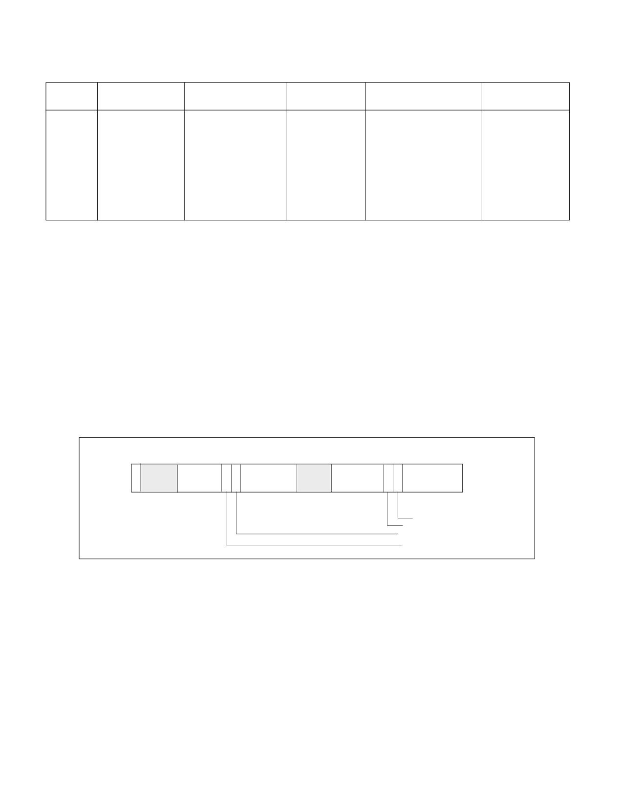
POWER AND THERMAL MANAGEMENT
Table 15-12. RAPL MSR Interfaces and RAPL Domains
Domain
Power Limit
Energy Status (Offset
Policy
Perf Status
Power Info
(Offset 0)
1)
(Offset 2)
(Offset 3)
(Offset 4)
PKG
MSR_PKG_POWER_
MSR_PKG_ENERGY_STA
RESERVED
MSR_PKG_PERF_STATUS
MSR_PKG_POWER_I
LIMIT
TUS
NFO
DRAM
MSR_DRAM_POWER
MSR_DRAM_ENERGY_S
RESERVED
MSR_DRAM_PERF_STATUS
MSR_DRAM_POWER
_LIMIT
TATUS
_INFO
PP0
MSR_PP0_POWER_
MSR_PP0_ENERGY_STA
MSR_PP0_POLICY
MSR_PP0_PERF_STATUS
RESERVED
LIMIT
TUS
PP1
MSR_PP1_POWER_
MSR_PP1_ENERGY_STA
MSR_PP1_POLICY
RESERVED
RESERVED
LIMIT
TUS
The presence of the optional MSR interfaces (the three right-most columns of Table 15-12) may be model-specific.
See Chapter 2, “Model-Specific Registers (MSRs)‚” in the Intel® 64 and IA-32 Architectures Software Developer’s
Manual, Volume 4, for details.
15.10.3 Package RAPL Domain
The MSR interfaces defined for the package RAPL domain are:
• MSR_PKG_POWER_LIMIT allows software to set power limits for the package and measurement attributes
associated with each limit,
• MSR_PKG_ENERGY_STATUS reports measured actual energy usage,
• MSR_PKG_POWER_INFO reports the package power range information for RAPL usage.
MSR_PKG_PERF_STATUS can report the performance impact of power limiting, but its availability may be model-
specific.
6362
5655
49 48 4746
3231
24 23
171615
14
0
L
O
Time window
Time window
Pkg Power Limit #2
Pkg Power Limit #1
C
Power Limit #2
Power Limit #1
K
Enable limit #1
Pkg clamping limit #1
Enable limit #2
Pkg clamping limit #2
Figure 15-36. MSR_PKG_POWER_LIMIT Register
MSR_PKG_POWER_LIMIT allows a software agent to define power limitation for the package domain. Power limita-
tion is defined in terms of average power usage (Watts) over a time window specified in MSR_PKG_POWER_LIMIT.
Two power limits can be specified, corresponding to time windows of different sizes. Each power limit provides inde-
pendent clamping control that would permit the processor cores to go below OS-requested state to meet the power
limits. A lock mechanism allow the software agent to enforce power limit settings. Once the lock bit is set, the
power limit settings are static and un-modifiable until next RESET.
The bit fields of MSR_PKG_POWER_LIMIT (Figure 15-36) are:
• Package Power Limit #1(bits 14:0): Sets the average power usage limit of the package domain corre-
sponding to time window # 1. The unit of this field is specified by the “Power Units” field of MSR_RAPL_POW-
ER_UNIT.
15-50
Vol. 3B

POWER AND THERMAL MANAGEMENT
• Enable Power Limit #1(bit 15): 0 = disabled; 1 = enabled.
• Package Clamping Limitation #1 (bit 16): Allow going below OS-requested P/T state setting during time
window specified by bits 23:17.
• Time Window for Power Limit #1 (bits 23:17): Indicates the time window for power limit #1
Time limit = 2^Y * (1.0 + Z/4.0) * Time_Unit
Here “Y” is the unsigned integer value represented. by bits 21:17, “Z” is an unsigned integer represented by
bits 23:22. “Time_Unit” is specified by the “Time Units” field of MSR_RAPL_POWER_UNIT.
• Package Power Limit #2(bits 46:32): Sets the average power usage limit of the package domain corre-
sponding to time window # 2. The unit of this field is specified by the “Power Units” field of MSR_RAPL_POW-
ER_UNIT.
• Enable Power Limit #2(bit 47): 0 = disabled; 1 = enabled.
• Package Clamping Limitation #2 (bit 48): Allow going below OS-requested P/T state setting during time
window specified by bits 23:17.
• Time Window for Power Limit #2 (bits 55:49): Indicates the time window for power limit #2
Time limit = 2^Y * (1.0 + Z/4.0) * Time_Unit
Here “Y” is the unsigned integer value represented. by bits 53:49, “Z” is an unsigned integer represented by
bits 55:54. “Time_Unit” is specified by the “Time Units” field of MSR_RAPL_POWER_UNIT. This field may have
a hard-coded value in hardware and ignores values written by software.
• Lock (bit 63): If set, all write attempts to this MSR are ignored until next RESET.
MSR_PKG_ENERGY_STATUS is a read-only MSR. It reports the actual energy use for the package domain. This
MSR is updated every ~1msec. It has a wraparound time of around 60 secs when power consumption is high, and
may be longer otherwise.
63
32 31
0
Reserved
Total Energy Consumed
Reserved
Figure 15-37. MSR_PKG_ENERGY_STATUS MSR
• Total Energy Consumed (bits 31:0): The unsigned integer value represents the total amount of energy
consumed since that last time this register is cleared. The unit of this field is specified by the “Energy Status
Units” field of MSR_RAPL_POWER_UNIT.
MSR_PKG_POWER_INFO is a read-only MSR. It reports the package power range information for RAPL usage. This
MSR provides maximum/minimum values (derived from electrical specification), thermal specification power of the
package domain. It also provides the largest possible time window for software to program the RAPL interface.
63
54 53
48 47 46
32
31 30
1615
14
0
Maximum Time window
Maximum Power
Minimum Power
Thermal Spec Power
Figure 15-38. MSR_PKG_POWER_INFO Register
• Thermal Spec Power (bits 14:0): The unsigned integer value is the equivalent of thermal specification power
of the package domain. The unit of this field is specified by the “Power Units” field of MSR_RAPL_POWER_UNIT.
Vol. 3B
15-51

POWER AND THERMAL MANAGEMENT
• Minimum Power (bits 30:16): The unsigned integer value is the equivalent of minimum power derived from
electrical spec of the package domain. The unit of this field is specified by the “Power Units” field of
MSR_RAPL_POWER_UNIT.
• Maximum Power (bits 46:32): The unsigned integer value is the equivalent of maximum power derived from
the electrical spec of the package domain. The unit of this field is specified by the “Power Units” field of
MSR_RAPL_POWER_UNIT.
• Maximum Time Window (bits 53:48): The unsigned integer value is the equivalent of largest acceptable
value to program the time window of MSR_PKG_POWER_LIMIT. The unit of this field is specified by the “Time
Units” field of MSR_RAPL_POWER_UNIT.
MSR_PKG_PERF_STATUS is a read-only MSR. It reports the total time for which the package was throttled due to
the RAPL power limits. Throttling in this context is defined as going below the OS-requested P-state or T-state. It
has a wrap-around time of many hours. The availability of this MSR is platform specific; see Chapter 2, “Model-
Specific Registers (MSRs)‚” in the Intel® 64 and IA-32 Architectures Software Developer’s Manual, Volume 4.
63
32 31
0
Reserved
Accumulated pkg throttled time
Reserved
Figure 15-39. MSR_PKG_PERF_STATUS MSR
• Accumulated Package Throttled Time (bits 31:0): The unsigned integer value represents the cumulative
time (since the last time this register is cleared) that the package has throttled. The unit of this field is specified
by the “Time Units” field of MSR_RAPL_POWER_UNIT.
15.10.4 PP0/PP1 RAPL Domains
The MSR interfaces defined for the PP0 and PP1 domains are identical in layout. Generally, PP0 refers to the
processor cores. The availability of PP1 RAPL domain interface is platform-specific. For a client platform, the PP1
domain refers to the power plane of a specific device in the uncore. For server platforms, the PP1 domain is not
supported, but its PP0 domain supports the MSR_PP0_PERF_STATUS interface.
• MSR_PP0_POWER_LIMIT/MSR_PP1_POWER_LIMIT allow software to set power limits for the respective power
plane domain.
• MSR_PP0_ENERGY_STATUS/MSR_PP1_ENERGY_STATUS report actual energy usage on a power plane.
• MSR_PP0_POLICY/MSR_PP1_POLICY allow software to adjust balance for respective power plane.
MSR_PP0_PERF_STATUS can report the performance impact of power limiting, but it is not available in client plat-
forms.
63
32 31
30
24 23
1716
15
14
0
L
O
Time window
C
Power Limit
Power Limit
K
Enable limit
Clamping limit
Figure 15-40. MSR_PP0_POWER_LIMIT/MSR_PP1_POWER_LIMIT Register
15-52
Vol. 3B

POWER AND THERMAL MANAGEMENT
MSR_PP0_POWER_LIMIT/MSR_PP1_POWER_LIMIT allow a software agent to define power limitation for the
respective power plane domain. A lock mechanism in each power plane domain allows the software agent to
enforce power limit settings independently. Once a lock bit is set, the power limit settings in that power plane are
static and un-modifiable until next RESET.
The bit fields of MSR_PP0_POWER_LIMIT/MSR_PP1_POWER_LIMIT (Figure 15-40) are:
• Power Limit (bits 14:0): Sets the average power usage limit of the respective power plane domain. The unit
of this field is specified by the “Power Units” field of MSR_RAPL_POWER_UNIT.
• Enable Power Limit (bit 15): 0 = disabled; 1 = enabled.
• Clamping Limitation (bit 16): Allow going below OS-requested P/T state setting during time window specified
by bits 23:17.
• Time Window for Power Limit (bits 23:17): Indicates the length of time window over which the power limit
#1 will be used by the processor. The numeric value encoded by bits 23:17 is represented by the product of
2^Y *F; where F is a single-digit decimal floating-point value between 1.0 and 1.3 with the fraction digit
represented by bits 23:22, Y is an unsigned integer represented by bits 21:17. The unit of this field is specified
by the “Time Units” field of MSR_RAPL_POWER_UNIT.
• Lock (bit 31): If set, all write attempts to the MSR and corresponding policy
MSR_PP0_POLICY/MSR_PP1_POLICY are ignored until next RESET.
MSR_PP0_ENERGY_STATUS/MSR_PP1_ENERGY_STATUS are read-only MSRs. They report the actual energy use
for the respective power plane domains. These MSRs are updated every ~1msec.
63
32 31
0
Reserved
Total Energy Consumed
Reserved
Figure 15-41. MSR_PP0_ENERGY_STATUS/MSR_PP1_ENERGY_STATUS MSR
• Total Energy Consumed (bits 31:0): The unsigned integer value represents the total amount of energy
consumed since the last time this register was cleared. The unit of this field is specified by the “Energy Status
Units” field of MSR_RAPL_POWER_UNIT.
MSR_PP0_POLICY/MSR_PP1_POLICY provide balance power policy control for each power plane by providing
inputs to the power budgeting management algorithm. On platforms that support PP0 (IA cores) and PP1 (uncore
graphic device), the default values give priority to the non-IA power plane. These MSRs enable the PCU to balance
power consumption between the IA cores and uncore graphic device.
63
5
4
0
Priority Level
Figure 15-42. MSR_PP0_POLICY/MSR_PP1_POLICY Register
• Priority Level (bits 4:0): Priority level input to the PCU for respective power plane. PP0 covers the IA
processor cores, PP1 covers the uncore graphic device. The value 31 is considered highest priority.
MSR_PP0_PERF_STATUS is a read-only MSR. It reports the total time for which the PP0 domain was throttled due
to the power limits. This MSR is supported only in server platform. Throttling in this context is defined as going
below the OS-requested P-state or T-state.
Vol. 3B
15-53

POWER AND THERMAL MANAGEMENT
63
32 31
0
Reserved
Accumulated PP0 throttled time
Reserved
Figure 15-43. MSR_PP0_PERF_STATUS MSR
• Accumulated PP0 Throttled Time (bits 31:0): The unsigned integer value represents the cumulative time
(since the last time this register is cleared) that the PP0 domain has throttled. The unit of this field is specified
by the “Time Units” field of MSR_RAPL_POWER_UNIT.
15.10.5 DRAM RAPL Domain
The MSR interfaces defined for the DRAM domains are supported only in the server platform. The MSR interfaces
are:
• MSR_DRAM_POWER_LIMIT allows software to set power limits for the DRAM domain and measurement
attributes associated with each limit.
• MSR_DRAM_ENERGY_STATUS reports measured actual energy usage.
• MSR_DRAM_POWER_INFO reports the DRAM domain power range information for RAPL usage.
• MSR_DRAM_PERF_STATUS can report the performance impact of power limiting.
63
32 31
30
24 23
1716
15
14
0
L
O
Time window
C
Power Limit
Power Limit
K
Enable limit
Clamping limit
Figure 15-44. MSR_DRAM_POWER_LIMIT Register
MSR_DRAM_POWER_LIMIT allows a software agent to define power limitation for the DRAM domain. Power limita-
tion is defined in terms of average power usage (Watts) over a time window specified in MSR_DRAM_POW-
ER_LIMIT. A power limit can be specified along with a time window. A lock mechanism allow the software agent to
enforce power limit settings. Once the lock bit is set, the power limit settings are static and un-modifiable until next
RESET.
The bit fields of MSR_DRAM_POWER_LIMIT (Figure 15-44) are:
• DRAM Power Limit #1(bits 14:0): Sets the average power usage limit of the DRAM domain corresponding to
time window # 1. The unit of this field is specified by the “Power Units” field of MSR_RAPL_POWER_UNIT.
• Enable Power Limit #1(bit 15): 0 = disabled; 1 = enabled.
• Time Window for Power Limit (bits 23:17): Indicates the length of time window over which the power limit
will be used by the processor. The numeric value encoded by bits 23:17 is represented by the product of 2^Y
*F; where F is a single-digit decimal floating-point value between 1.0 and 1.3 with the fraction digit represented
by bits 23:22, Y is an unsigned integer represented by bits 21:17. The unit of this field is specified by the “Time
Units” field of MSR_RAPL_POWER_UNIT.
• Lock (bit 31): If set, all write attempts to this MSR are ignored until next RESET.
15-54
Vol. 3B

POWER AND THERMAL MANAGEMENT
MSR_DRAM_ENERGY_STATUS is a read-only MSR. It reports the actual energy use for the DRAM domain. This MSR
is updated every ~1msec.
63
32 31
0
Reserved
Total Energy Consumed
Reserved
Figure 15-45. MSR_DRAM_ENERGY_STATUS MSR
• Total Energy Consumed (bits 31:0): The unsigned integer value represents the total amount of energy
consumed since that last time this register is cleared. The unit of this field is specified by the “Energy Status
Units” field of MSR_RAPL_POWER_UNIT.
MSR_DRAM_POWER_INFO is a read-only MSR. It reports the DRAM power range information for RAPL usage. This
MSR provides maximum/minimum values (derived from electrical specification), thermal specification power of the
DRAM domain. It also provides the largest possible time window for software to program the RAPL interface.
63
54 53
48 47 46
32
31 30
1615
14
0
Maximum Time window
Maximum Power
Minimum Power
Thermal Spec Power
Figure 15-46. MSR_DRAM_POWER_INFO Register
• Thermal Spec Power (bits 14:0): The unsigned integer value is the equivalent of thermal specification power
of the DRAM domain. The unit of this field is specified by the “Power Units” field of MSR_RAPL_POWER_UNIT.
• Minimum Power (bits 30:16): The unsigned integer value is the equivalent of minimum power derived from
electrical spec of the DRAM domain. The unit of this field is specified by the “Power Units” field of
MSR_RAPL_POWER_UNIT.
• Maximum Power (bits 46:32): The unsigned integer value is the equivalent of maximum power derived from
the electrical spec of the DRAM domain. The unit of this field is specified by the “Power Units” field of
MSR_RAPL_POWER_UNIT.
• Maximum Time Window (bits 53:48): The unsigned integer value is the equivalent of largest acceptable
value to program the time window of MSR_DRAM_POWER_LIMIT. The unit of this field is specified by the “Time
Units” field of MSR_RAPL_POWER_UNIT.
MSR_DRAM_PERF_STATUS is a read-only MSR. It reports the total time for which the package was throttled due to
the RAPL power limits. Throttling in this context is defined as going below the OS-requested P-state or T-state. It
has a wrap-around time of many hours. The availability of this MSR is platform specific; see Chapter 2, “Model-
Specific Registers (MSRs)‚” in the Intel® 64 and IA-32 Architectures Software Developer’s Manual, Volume 4.
63
32 31
0
Reserved
Accumulated DRAM throttled time
Reserved
Figure 15-47. MSR_DRAM_PERF_STATUS MSR
Vol. 3B
15-55
POWER AND THERMAL MANAGEMENT
• Accumulated Package Throttled Time (bits 31:0): The unsigned integer value represents the cumulative
time (since the last time this register is cleared) that the DRAM domain has throttled. The unit of this field is
specified by the “Time Units” field of MSR_RAPL_POWER_UNIT.
15-56
Vol. 3B

CHAPTER 16
MACHINE-CHECK ARCHITECTURE
This chapter describes the machine-check architecture and machine-check exception mechanism found in the
Pentium 4, Intel Xeon, Intel Atom, and P6 family processors. See Chapter 6, “Interrupt 18—Machine-Check Excep-
tion (#MC),” for more information on machine-check exceptions. A brief description of the Pentium processor’s
machine check capability is also given.
Additionally, a signaling mechanism for software to respond to hardware corrected machine check error is covered.
16.1
MACHINE-CHECK ARCHITECTURE
The Pentium 4, Intel Xeon, Intel Atom, and P6 family processors implement a machine-check architecture that
provides a mechanism for detecting and reporting hardware (machine) errors, such as: system bus errors, ECC
errors, parity errors, cache errors, and TLB errors. It consists of a set of model-specific registers (MSRs) that are
used to set up machine checking and additional banks of MSRs used for recording errors that are detected.
The processor signals the detection of an uncorrected machine-check error by generating a machine-check excep-
tion (#MC), which is an abort class exception. The implementation of the machine-check architecture does not
ordinarily permit the processor to be restarted reliably after generating a machine-check exception. However, the
machine-check-exception handler can collect information about the machine-check error from the machine-check
MSRs.
Starting with 45 nm Intel 64 processor on which CPUID reports DisplayFamily_DisplayModel as 06H_1AH; see the
CPUID instruction in Chapter 3, “Instruction Set Reference, A-L,” in the Intel® 64 and IA-32 Architectures Software
Developer’s Manual, Volume 2A. The processor can report information on corrected machine-check errors and
deliver a programmable interrupt for software to respond to MC errors, referred to as corrected machine-check
error interrupt (CMCI). See Section 16.5 for details.
Intel 64 processors supporting machine-check architecture and CMCI may also support an additional enhance-
ment, namely, support for software recovery from certain uncorrected recoverable machine check errors. See
Section 16.6 for details.
16.2
COMPATIBILITY WITH PENTIUM PROCESSOR
The Pentium 4, Intel Xeon, Intel Atom, and P6 family processors support and extend the machine-check exception
mechanism introduced in the Pentium processor. The Pentium processor reports the following machine-check
errors:
• Data parity errors during read cycles.
• Unsuccessful completion of a bus cycle.
The above errors are reported using the P5_MC_TYPE and P5_MC_ADDR MSRs (implementation specific for the
Pentium processor). Use the RDMSR instruction to read these MSRs. See Chapter 2, “Model-Specific Registers
(MSRs)‚” in the Intel® 64 and IA-32 Architectures Software Developer’s Manual, Volume 4, for the addresses.
The machine-check error reporting mechanism that Pentium processors use is similar to that used in Pentium 4,
Intel Xeon, Intel Atom, and P6 family processors. When an error is detected, it is recorded in P5_MC_TYPE and
P5_MC_ADDR; the processor then generates a machine-check exception (#MC).
See Section 16.3.3, “Mapping of the Pentium Processor Machine-Check Errors to the Machine-Check Architecture,”
and Section 16.10.2, “Pentium Processor Machine-Check Exception Handling,” for information on compatibility
between machine-check code written to run on the Pentium processors and code written to run on P6 family
processors.
Vol. 3B
16-1

MACHINE-CHECK ARCHITECTURE
16.3
MACHINE-CHECK MSRS
Machine check MSRs in the Pentium 4, Intel Atom, Intel Xeon, and P6 family processors consist of a set of global
control and status registers and several error-reporting register banks. See Figure 16-1.
Global Control MSRs
Error-Reporting Bank Registers
(One Set for Each Hardware Unit)
63
0
63
0
IA32_MCG_CAP MSR
IA32_MCi_CTL MSR
63
0
63
0
IA32_MCG_STATUS MSR
IA32_MCi_STATUS MSR
63
0
63
0
IA32_MCG_CTL MSR
IA32_MCi_ADDR MSR
63
0
63
0
IA32_MCG_EXT_CTL MSR
IA32_MCi_MISC MSR
63
0
IA32_MCi_CTL2 MSR
Figure 16-1. Machine-Check MSRs
Each error-reporting bank is associated with a specific hardware unit (or group of hardware units) in the processor.
Use RDMSR and WRMSR to read and to write these registers.
16.3.1 Machine-Check Global Control MSRs
The machine-check global control MSRs include the IA32_MCG_CAP, IA32_MCG_STATUS, and optionally IA32_MC-
G_CTL and IA32_MCG_EXT_CTL. See Chapter 2, “Model-Specific Registers (MSRs),” in the Intel® 64 and IA-32
Architectures Software Developer’s Manual, Volume 4, for the addresses of these registers.
16.3.1.1 IA32_MCG_CAP MSR
The IA32_MCG_CAP MSR is a read-only register that provides information about the machine-check architecture of
the processor. Figure 16-2 shows the layout of the register.
16-2
Vol. 3B