Intel 64 and IA-32 Architectures. Software Developer’s Manual (Collection, 2023) - page 49
MULTIPLE-PROCESSOR MANAGEMENT
• Sub-leaf index 0 (ECX= 0 as input) provides enumeration parameters to extract the LOGICAL_PROCESSOR_ID
sub-field of x2APIC ID. If EAX = 0BH or 1FH, and ECX =0 is specified as input when executing CPUID,
CPUID.(EAX=0BH or 1FH, ECX=0):EAX[4:0] reports a value (a right-shift count) that allow software to extract
part of x2APIC ID to distinguish the next higher topological entities above the LOGICAL_PROCESSOR_ID
domain. This value also corresponds to the bit-width of the sub-field of x2APIC ID corresponding the hierar-
chical domain with sub-leaf index 0.
• For each subsequent higher sub-leaf index m, CPUID.(EAX=0BH or 1FH, ECX=m):EAX[4:0] reports the right-
shift count that will allow software to extract part of x2APIC ID to distinguish higher-domain topological
entities. This means the right-shift value at of sub-leaf m, corresponds to the least significant (m+1) sub-fields
of the 32-bit x2APIC ID.
Example 9-17. BitWidth Determination of x2APIC ID Sub-fields
For m = 0, m < N, m ++;
{
cumulative_width[m] = CPUID.(EAX=0BH or 1FH, ECX= m): EAX[4:0]; }
BitWidth[0] = cumulative_width[0];
For m = 1, m < N, m ++;
BitWidth[m] = cumulative_width[m] - cumulative_width[m-1];
NOTE
CPUID leaf 1FH is a preferred superset to leaf 0BH. Leaf 1FH defines additional domain types, and
it must be parsed by an algorithm that can handle the addition of future domain types.
Previously, only the following encoding of hierarchical domain types were defined: 0 (invalid), 1 (logical processor),
and 2 (core). With the additional hierarchical domain types available (see Section 9.9.1, “Hierarchical Mapping of
Shared Resources,” and Figure 9-5, “Generalized Seven-Domain Interpretation of the APIC ID” ) software must not
assume any “domain type” encoding value to be related to any sub-leaf index, except sub-leaf 0.
Example 9-18. Support Routines for Identifying Package, Die, Core, and Logical Processors from 32-bit x2APIC ID
a.
Derive the extraction bitmask for logical processors in a processor core and associated mask offset for different
cores.
//
// This example shows how to enumerate CPU topology domain types (domain types may or may not be known/supported by the
software)
//
// Below is the list of sample domain types used in the example.
// Refer to the CPUID Leaf 1FH definition for the actual domain type numbers: “V2 Extended Topology Enumeration Leaf (Initial EAX
Value = 1FH)” .
//
// LOGICAL PROCESSOR
// CORE
// MODULE
// TILE
// DIE
// PACKAGE
//
// The example shows how to identify and derive the extraction bitmask for the domains with identify type
LOGICAL_PROCESSOR_ID/CORE_ID/DIE_ID/PACKAGE_ID
//
int DeriveLogical_Processor_Mask_Offsets (void)
{
Vol. 3A
9-37
MULTIPLE-PROCESSOR MANAGEMENT
IF (!HWMTSupported()) return -1;
execute cpuid with EAX = 0BH or 1FH, ECX = 0;
IF (returned domain type encoding in EXC[15:8] does not match LOGICAL_PROCESSOR_ID) return -1;
Mask_Logical_Processor_shift = EAX[4:0];
//# bits shift right of APIC ID to distinguish different cores, note this can be a shift
// of zero if there is only one logical processor per core.
Logical Processor Mask =~( (-1) << Mask_Logical_Processor_shift);
//shift left to derive extraction bitmask for
// LOGICAL_PROCESSOR_ID
return 0;
}
b.
Derive the extraction bitmask for processor cores in a physical processor package and associated mask offset for
different packages.
int DeriveCore_Mask_Offsets (void)
{
IF (!HWMTSupported()) return -1;
execute cpuid with EAX = 0BH or 1FH, ECX = 0;
WHILE( ECX[15:8] ) {
//domain type encoding is valid
Mask_last_known_shift = EAX[4:0]
IF (returned domain type encoding in ECX[15:8] matches CORE) {
Mask_Core_shift = EAX[4:0];
}
ELSE IF (returned domain type encoding in ECX[15:8] matches DIE {
Mask_Die_shift = EAX[4:0];
}
//
// Keep enumerating. Check if the next domain is the desired domain and if not, keep enumerating until you reach a known
// domain or the invalid domain (“0” domain type). If there are more domains between DIE and PACKAGE, the unknown
// domains will be ignored and treated as an extension of the last known domain (i.e., DIE in this case).
//
ECX++;
execute cpuid with EAX = 0BH or 1FH;
}
COREPlusLogical_Processor_MASK = ~( (-1) << Mask_Core_shift);
DIEPlusCORE_MASK = ~( (-1) << Mask_Die_shift);
//
// Treat domains between DIE and physical package as an extension of DIE for software choosing not to implement or recognize
// these unknown domains.
//
CORE_MASK = COREPlusLogical_Processor_MASK ^ Logical Processor Mask;
DIE_MASK = DIEPlusCORE_MASK ^ COREPlusLogical_Processor_MASK;
PACKAGE_MASK = (-1) << Mask_last_known_shift;
return -1;
}
9-38
Vol. 3A

MULTIPLE-PROCESSOR MANAGEMENT
9.9.3
Hierarchical ID of Logical Processors in an MP System
For Intel 64 and IA-32 processors, system hardware establishes an 8-bit initial APIC ID (or 32-bit APIC ID if the
processor supports CPUID leaf 0BH) that is unique for each logical processor following power-up or RESET (see
Section 9.6.1). Each logical processor on the system is allocated an initial APIC ID. BIOS may implement features
that tell the OS to support less than the total number of logical processors on the system bus. Those logical proces-
sors that are not available to applications at runtime are halted during the OS boot process. As a result, the number
valid local APIC_IDs that can be queried by affinitizing-current-thread-context (See Example 9-23) is limited to the
number of logical processors enabled at runtime by the OS boot process.
Table 9-2 shows an example of the 8-bit APIC IDs that are initially reported for logical processors in a system with
four Intel Xeon MP processors that support Intel Hyper-Threading Technology (a total of 8 logical processors, each
physical package has two processor cores and supports Intel Hyper-Threading Technology). Of the two logical
processors within a Intel Xeon processor MP, logical processor 0 is designated the primary logical processor and
logical processor 1 as the secondary logical processor.
LOGICAL_PROCESSOR_ID
CORE_ID
T0
T1
T0
T1
T0
T1
T0
T1
PACKAGE_ID
Core 0
Core 1
Core 0
Core 1
Package 0
Package 1
Figure 9-7. Topological Relationships Between Hierarchical IDs in a Hypothetical MP Platform
Table 9-2. Initial APIC IDs for the Logical Processors in a System that has Four Intel Xeon MP Processors Supporting
Intel Hyper-Threading Technology1
Initial APIC ID
PACKAGE_ID
CORE_ID
LOGICAL_PROCESSOR_ID
0H
0H
0H
0H
1H
0H
0H
1H
2H
1H
0H
0H
3H
1H
0H
1H
4H
2H
0H
0H
5H
2H
0H
1H
6H
3H
0H
0H
7H
3H
0H
1H
NOTE:
1. Because information on the number of processor cores in a physical package was not available in early single-core processors sup-
porting Intel Hyper-Threading Technology, the CORE_ID can be treated as 0.
Table 9-3 shows the initial APIC IDs for a hypothetical situation with a dual processor system. Each physical
package providing two processor cores, and each processor core also supporting Intel Hyper-Threading Tech-
nology.
Vol. 3A
9-39

MULTIPLE-PROCESSOR MANAGEMENT
Table 9-3. Initial APIC IDs for the Logical Processors in a System that has Two Physical Processors Supporting Dual-
Core and Intel Hyper-Threading Technology
Initial APIC ID
PACKAGE_ID
CORE_ID
LOGICAL_PROCESSOR_ID
0H
0H
0H
0H
1H
0H
0H
1H
2H
0H
1H
0H
3H
0H
1H
1H
4H
1H
0H
0H
5H
1H
0H
1H
6H
1H
1H
0H
7H
1H
1H
1H
9.9.3.1
Hierarchical ID of Logical Processors with x2APIC ID
Table 9-4 shows an example of possible x2APIC ID assignments for a dual processor system that support x2APIC.
Each physical package providing four processor cores, and each processor core also supporting Intel Hyper-
Threading Technology. Note that the x2APIC ID need not be contiguous in the system.
Table 9-4. Example of Possible x2APIC ID Assignment in a System that has Two Physical Processors Supporting
x2APIC and Intel Hyper-Threading Technology
x2APIC ID
PACKAGE_ID
CORE_ID
LOGICAL_PROCESSOR_ID
0H
0H
0H
0H
1H
0H
0H
1H
2H
0H
1H
0H
3H
0H
1H
1H
4H
0H
2H
0H
5H
0H
2H
1H
6H
0H
3H
0H
7H
0H
3H
1H
10H
1H
0H
0H
11H
1H
0H
1H
12H
1H
1H
0H
13H
1H
1H
1H
14H
1H
2H
0H
15H
1H
2H
1H
16H
1H
3H
0H
17H
1H
3H
1H
9-40
Vol. 3A
MULTIPLE-PROCESSOR MANAGEMENT
9.9.4
Algorithm for Three-Domain Mappings of APIC_ID
Software can gather the initial APIC_IDs for each logical processor supported by the operating system at runtime1
and extract identifiers corresponding to the three domains of sharing topology (package, core, and logical
processor). The three-domain algorithms below focus on a non-clustered MP system for simplicity. They do not
assume APIC IDs are contiguous or that all logical processors on the platform are enabled.
Intel supports multi-threading systems where all physical processors report identical values in CPUID leaf 0BH,
CPUID.1:EBX[23:16]), CPUID.42:EAX[31:26], and CPUID.43:EAX[25:14]. The algorithms below assume the
target system has symmetry across physical package boundaries with respect to the number of logical processors
per package, number of cores per package, and cache topology within a package.
Software can choose to assume three-domain hierarchy if it was developed to understand only three domains.
However, software implementation needs to ensure it does not break if it runs on systems that have more domains
in the hierarchy even if it does not recognize them.
The extraction algorithm (for three-domain mappings from an APIC ID) uses the general procedure depicted in
Example 9-19, and is supplemented by more detailed descriptions on the derivation of topology enumeration
parameters for extraction bit masks:
1.
Detect hardware multi-threading support in the processor.
2.
Derive a set of bit masks that can extract the sub ID of each hierarchical domain of the topology. The algorithm
to derive extraction bit masks for LOGICAL_PROCESSOR_ID/CORE_ID/PACKAGE_ID differs based on APIC ID
is 32-bit (see step 3 below) or 8-bit (see step 4 below).
3.
If the processor supports CPUID leaf 0BH, each APIC ID contains a 32-bit value, the topology enumeration
parameters needed to derive three-domain extraction bit masks are:
a. Query the right-shift value for the LOGICAL_PROCESSOR_ID domain of the topology using CPUID leaf 0BH
with ECX =0H as input. The number of bits to shift-right on x2APIC ID (EAX[4:0]) can distinguish different
higher-domain entities above logical processor in the same physical package. This is also the width of the
bit mask to extract the LOGICAL_PROCESSOR_ID. The shift value may be 0 and enumerate no logical
processor bit mask to create. A platform where cores only have one logical processor are not required to
enumerate a separate bit layout for logical processor, and the lowest bits may only identify the core (where
core and logical processor are then synonymous).
b. Enumerate until the desired domain is found (i.e., processor cores). Determine if the next domain is the
expected domain. If the next domain is not known to the software, keep enumerating until the next known
or the last domain. Software should use the previous domain before this to represent the last previously
known domain (i.e., processor cores). If the software does not recognize or implement certain hierarchical
domains, it should assume these unknown domains as an extension of the last known domain.
c. Query CPUID leaf 0BH for the amount of bit shift to distinguish next higher-domain entities (e.g., physical
processor packages) in the system. This describes an explicit three-domain-topology situation for
commonly available processors. Consult Example 9-17 to adapt to situations beyond a three-domain
topology of a physical processor. The width of the extraction bit mask can be used to derive the cumulative
extraction bitmask to extract the sub IDs of logical processors (including different processor cores) in the
same physical package. The extraction bit mask to distinguish merely different processor cores can be
derived by xor’ing the logical processor extraction bit mask from the cumulative extraction bit mask.
d. Query the 32-bit x2APIC ID for the logical processor where the current thread is executing.
e. Derive the extraction bit masks corresponding to LOGICAL_PROCESSOR_ID, CORE_ID, and PACKAGE_ID,
starting from LOGICAL_PROCESSOR_ID.
f. Apply each extraction bit mask to the 32-bit x2APIC ID to extract sub-field IDs.
1.
As noted in Section 9.6 and Section 9.9.3, the number of logical processors supported by the OS at runtime may be less than the
total number logical processors available in the platform hardware.
2.
Maximum number of addressable ID for processor cores in a physical processor is obtained by executing CPUID with EAX=4 and a
valid ECX index. The ECX index starts at 0.
3.
Maximum number addressable ID for processor cores sharing the target cache level is obtained by executing CPUID with EAX = 4
and the ECX index corresponding to the target cache level.
Vol. 3A
9-41
MULTIPLE-PROCESSOR MANAGEMENT
4. If the processor does not support CPUID leaf 0BH, each initial APIC ID contains an 8-bit value, the topology
enumeration parameters needed to derive extraction bit masks are:
a. Query the size of address space for sub IDs that can accommodate logical processors in a physical
processor package. This size parameters (CPUID.1:EBX[23:16]) can be used to derive the width of an
extraction bitmask to enumerate the sub IDs of different logical processors in the same physical package.
b. Query the size of address space for sub IDs that can accommodate processor cores in a physical processor
package. This size parameters can be used to derive the width of an extraction bitmask to enumerate the
sub IDs of processor cores in the same physical package.
c. Query the 8-bit initial APIC ID for the logical processor where the current thread is executing.
d. Derive the extraction bit masks using respective address sizes corresponding to LOGICAL_PROCESSOR_ID,
CORE_ID, and PACKAGE_ID, starting from LOGICAL_PROCESSOR_ID.
e. Apply each extraction bit mask to the 8-bit initial APIC ID to extract sub-field IDs.
Example 9-19. Support Routines for Detecting Hardware Multi-Threading and Identifying the Relationships Between Package,
Core, and Logical Processors
1.
Detect support for Hardware Multi-Threading Support in a processor.
// Returns a non-zero value if CPUID reports the presence of hardware multi-threading
// support in the physical package where the current logical processor is located.
// This does not guarantee BIOS or OS will enable all logical processors in the physical
// package and make them available to applications.
// Returns zero if hardware multi-threading is not present.
#define HWMT_BIT 10000000H
unsigned int HWMTSupported(void)
{
// ensure cpuid instruction is supported
execute cpuid with eax = 0 to get vendor string
execute cpuid with eax = 1 to get feature flag and signature
// Check to see if this a Genuine Intel Processor
if (vendor string EQ GenuineIntel) {
return (feature_flag_edx & HWMT_BIT); // bit 28
}
return 0;
}
Example 9-20. Support Routines for Identifying Package, Core, and Logical Processors from 32-bit x2APIC ID
a.
Derive the extraction bitmask for logical processors in a processor core and associated mask offset for different
cores.
int DeriveLogical_Processor_Mask_Offsets (void)
{
if (!HWMTSupported()) return -1;
execute cpuid with eax = 11, ECX = 0;
If (returned domain type encoding in ECX[15:8] does not match logical processor) return -1;
Mask_Logical_Processor_shift = EAX[4:0];
// # bits shift right of APIC ID to distinguish different cores, note this can be a shift
// of zero if there is only one logical processor per core.
Logical Processor Mask = ~( (-1) << Mask_Logical_Processor_shift); // shift left to derive extraction bitmask for
// LOGICAL_PROCESSOR_ID
9-42
Vol. 3A
MULTIPLE-PROCESSOR MANAGEMENT
return 0;
}
b.
Derive the extraction bitmask for processor cores in a physical processor package and associated mask offset for
different packages.
int DeriveCore_Mask_Offsets (void)
{
if (!HWMTSupported()) return -1;
execute cpuid with eax = 11, ECX = 0;
while( ECX[15:8] ) {
// domain type encoding is valid
Mask_Core_shift = EAX[4:0];
// needed to distinguish different physical packages
ECX ++;
execute cpuid with eax = 11;
}
COREPlusLogical_Processor_MASK = ~( (-1) << Mask_Core_shift);
// treat domains between core and physical package as a core for software choosing not to implement or recognize
// these unknown domains
CORE_MASK = COREPlusLogical_Processor_MASK ^ Logical Processor Mask;
PACKAGE_MASK = (-1) << Mask_Core_shift;
return -1;
}
c.
Query the x2APIC ID of a logical processor.
APIC_IDs for each logical processor.
unsigned char Getx2APIC_ID (void)
{
unsigned reg_edx = 0;
execute cpuid with eax = 11, ECX = 0
store returned value of edx
return (unsigned) (reg_edx) ;
}
Example 9-21. Support Routines for Identifying Package, Core, and Logical Processors from 8-bit Initial APIC ID
a.
Find the size of address space for logical processors in a physical processor package.
#define NUM_LOGICAL_BITS 00FF0000H
// Use the mask above and CPUID.1.EBX[23:16] to obtain the max number of addressable IDs
// for logical processors in a physical package,
//Returns the size of address space of logical processors in a physical processor package;
// Software should not assume the value to be a power of 2.
unsigned char MaxLPIDsPerPackage(void)
{
if (!HWMTSupported()) return 1;
execute cpuid with eax = 1
store returned value of ebx
return (unsigned char) ((reg_ebx & NUM_LOGICAL_BITS) >> 16);
}
Vol. 3A
9-43
MULTIPLE-PROCESSOR MANAGEMENT
b.
Find the size of address space for processor cores in a physical processor package.
// Returns the max number of addressable IDs for processor cores in a physical processor package;
// Software should not assume cpuid reports this value to be a power of 2.
unsigned MaxCoreIDsPerPackage(void)
{
if (!HWMTSupported()) return (unsigned char) 1;
if cpuid supports leaf number 4
{ // we can retrieve multi-core topology info using leaf 4
execute cpuid with eax = 4, ecx = 0
store returned value of eax
return (unsigned) ((reg_eax >> 26) +1);
}
else // must be a single-core processor
return 1;
}
c.
Query the initial APIC ID of a logical processor.
#define INITIAL_APIC_ID_BITS FF000000H // CPUID.1.EBX[31:24] initial APIC ID
// Returns the 8-bit unique initial APIC ID for the processor running the code.
// Software can use OS services to affinitize the current thread to each logical processor
// available under the OS to gather the initial APIC_IDs for each logical processor.
unsigned GetInitAPIC_ID (void)
{
unsigned int reg_ebx = 0;
execute cpuid with eax = 1
store returned value of ebx
return (unsigned) ((reg_ebx & INITIAL_APIC_ID_BITS) >> 24;
}
d.
Find the width of an extraction bitmask from the maximum count of the bit-field (address size).
// Returns the mask bit width of a bit field from the maximum count that bit field can represent.
// This algorithm does not assume ‘address size’ to have a value equal to power of 2.
// Address size for LOGICAL_PROCESSOR_ID can be calculated from MaxLPIDsPerPackage()/MaxCoreIDsPerPackage()
// Then use the routine below to derive the corresponding width of logical processor extraction bitmask
// Address size for CORE_ID is MaxCoreIDsPerPackage(),
// Derive the bitwidth for CORE extraction mask similarly
unsigned FindMaskWidth(Unsigned Max_Count)
{unsigned int mask_width, cnt = Max_Count;
__asm {
mov eax, cnt
mov ecx, 0
mov mask_width, ecx
dec eax
bsr cx, ax
jz next
inc cx
mov mask_width, ecx
next:
mov eax, mask_width
9-44
Vol. 3A
MULTIPLE-PROCESSOR MANAGEMENT
}
return mask_width;
}
e.
Extract a sub ID from an 8-bit full ID, using address size of the sub ID and shift count.
// The routine below can extract LOGICAL_PROCESSOR_ID, CORE_ID, and PACKAGE_ID respectively from the init APIC_ID
// To extract LOGICAL_PROCESSOR_ID, MaxSubIDvalue is set to the address size of LOGICAL_PROCESSOR_ID, Shift_Count = 0
// To extract CORE_ID, MaxSubIDvalue is the address size of CORE_ID, Shift_Count is width of logical processor extraction bitmask.
// Returns the value of the sub ID, this is not a zero-based value
Unsigned char GetSubID(unsigned char Full_ID, unsigned char MaxSubIDvalue, unsigned char Shift_Count)
{
MaskWidth = FindMaskWidth(MaxSubIDValue);
MaskBits = ((uchar) (FFH << Shift_Count)) ^ ((uchar) (FFH << Shift_Count + MaskWidth)) ;
SubID = Full_ID & MaskBits;
Return SubID;
}
Software must not assume local APIC_ID values in an MP system are consecutive. Non-consecutive local APIC_IDs
may be the result of hardware configurations or debug features implemented in the BIOS or OS.
An identifier for each hierarchical domain can be extracted from an 8-bit APIC_ID using the support routines illus-
trated in Example 9-21. The appropriate bit mask and shift value to construct the appropriate bit mask for each
domain must be determined dynamically at runtime.
9.9.5
Identifying Topological Relationships in an MP System
To detect the number of physical packages, processor cores, or other topological relationships in a MP system, the
following procedures are recommended:
• Extract the three-domain identifiers from the APIC ID of each logical processor enabled by system software.
The sequence is as follows (see the pseudo code shown in Example 9-22 and support routines shown in
Example 9-19):
• The extraction start from the right-most bit field, corresponding to LOGICAL_PROCESSOR_ID, the
innermost hierarchy in a three-domain topology (See Figure 9-7). For the right-most bit field, the shift
value of the working mask is zero. The width of the bit field is determined dynamically using the
maximum number of logical processor per core, which can be derived from information provided from
CPUID.
• To extract the next bit-field, the shift value of the working mask is determined from the width of the bit
mask of the previous step. The width of the bit field is determined dynamically using the maximum
number of cores per package.
• To extract the remaining bit-field, the shift value of the working mask is determined from the maximum
number of logical processor per package. So the remaining bits in the APIC ID (excluding those bits
already extracted in the two previous steps) are extracted as the third identifier. This applies to a non-
clustered MP system, or if there is no need to distinguish between PACKAGE_ID and CLUSTER_ID.
If there is need to distinguish between PACKAGE_ID and CLUSTER_ID, PACKAGE_ID can be extracted
using an algorithm similar to the extraction of CORE_ID, assuming the number of physical packages in
each node of a clustered system is symmetric.
• Assemble the three-domain identifiers of LOGICAL_PROCESSOR_ID, CORE_ID, PACKAGE_IDs into arrays for
each enabled logical processor. This is shown in Example 9-23a.
• To detect the number of physical packages: use PACKAGE_ID to identify those logical processors that reside in
the same physical package. This is shown in Example 9-23b. This example also depicts a technique to construct
a mask to represent the logical processors that reside in the same package.
Vol. 3A
9-45
MULTIPLE-PROCESSOR MANAGEMENT
• To detect the number of processor cores: use CORE_ID to identify those logical processors that reside in the
same core. This is shown in Example 9-23. This example also depicts a technique to construct a mask to
represent the logical processors that reside in the same core.
In Example 9-22, the numerical ID value can be obtained from the value extracted with the mask by shifting it right
by shift count. Algorithms below do not shift the value. The assumption is that the SubID values can be compared
for equivalence without the need to shift.
Example 9-22. Pseudo Code Depicting Three-Domain Extraction Algorithm
For Each local_APIC_ID{
// Calculate Logical Processor Mask, the bit mask pattern to extract LOGICAL_PROCESSOR_ID,
// Logical Processor Mask is determined using topology enumertaion parameters
// from CPUID leaf 0BH (Example 9-20);
// otherwise, Logical Processor Mask is determined using CPUID leaf 01H and leaf 04H (Example 9-21).
// This algorithm assumes there is symmetry across core boundary, i.e., each core within a
// package has the same number of logical processors
// LOGICAL_PROCESSOR_ID always starts from bit 0, corresponding to the right-most bit-field
LOGICAL_PROCESSOR_ID = APIC_ID & Logical Processor Mask;
// Extract CORE_ID:
// Core Mask is determined in Example 9-20 or Example 9-21
CORE_ID = (APIC_ID & Core Mask);
// Extract PACKAGE_ID:
// Assume single cluster.
// Shift out the mask width for maximum logical processors per package
// Package Mask is determined in Example 9-20 or Example 9-21
PACKAGE_ID = (APIC_ID & Package Mask) ;
}
Example 9-23. Compute the Number of Packages, Cores, and Processor Relationships in a MP System
a) Assemble lists of PACKAGE_ID, CORE_ID, and LOGICAL_PROCESSOR_ID of each enabled logical processors
// The BIOS and/or OS may limit the number of logical processors available to applications after system boot.
// The below algorithm will compute topology for the processors visible to the thread that is computing it.
// Extract the 3-domains of IDs on every processor.
// SystemAffinity is a bitmask of all the processors started by the OS. Use OS specific APIs to obtain it.
// ThreadAffinityMask is used to affinitize the topology enumeration thread to each processor using OS specific APIs.
// Allocate per processor arrays to store the Package_ID, Core_ID, and LOGICAL_PROCESSOR_ID for every started processor.
ThreadAffinityMask = 1;
ProcessorNum = 0;
while (ThreadAffinityMask ≠ 0 && ThreadAffinityMask <= SystemAffinity) {
// Check to make sure we can utilize this processor first.
if (ThreadAffinityMask & SystemAffinity){
Set thread to run on the processor specified in ThreadAffinityMask
Wait if necessary and ensure thread is running on specified processor
APIC_ID = GetAPIC_ID(); // 32 bit ID in Example 9-20 or 8-bit ID in Example 9-21
Extract the Package_ID, Core_ID, and LOGICAL_PROCESSOR_ID as explained in three domain extraction
algorithm of Example 9-22
PackageID[ProcessorNUM] = PACKAGE_ID;
CoreID[ProcessorNum] = CORE_ID;
9-46
Vol. 3A
MULTIPLE-PROCESSOR MANAGEMENT
LOGICAL_PROCESSOR_ID[ProcessorNum] = LOGICAL_PROCESSOR_ID;
ProcessorNum++;
}
ThreadAffinityMask <<= 1;
}
NumStartedLPs = ProcessorNum;
b) Using the list of PACKAGE_ID to count the number of physical packages in a MP system and construct, for each package, a multi-bit
mask corresponding to those logical processors residing in the same package.
// Compute the number of packages by counting the number of processors with unique PACKAGE_IDs in the PackageID array.
// Compute the mask of processors in each package.
// PackageIDBucket is an array of unique PACKAGE_ID values. Allocate an array of NumStartedLPs count of entries in this array.
// PackageProcessorMask is a corresponding array of the bit mask of processors belonging to the same package, these are
// processors with the same PACKAGE_ID.
// The algorithm below assumes there is symmetry across package boundary if more than one socket is populated in an MP
//system.
// Bucket Package IDs and compute processor mask for every package.
PackageNum = 1;
PackageIDBucket[0] = PackageID[0];
ProcessorMask = 1;
PackageProcessorMask[0] = ProcessorMask;
For (ProcessorNum = 1; ProcessorNum < NumStartedLPs; ProcessorNum++) {
ProcessorMask << = 1;
For (i=0; i < PackageNum; i++) {
// we may be comparing bit-fields of logical processors residing in different
// packages, the code below assume package symmetry
If (PackageID[ProcessorNum] = PackageIDBucket[i]) {
PackageProcessorMask[i] |= ProcessorMask;
Break; // found in existing bucket, skip to next iteration
}
}
if (i =PackageNum) {
//PACKAGE_ID did not match any bucket, start new bucket
PackageIDBucket[i] = PackageID[ProcessorNum];
PackageProcessorMask[i] = ProcessorMask;
PackageNum++;
}
}
// PackageNum has the number of Packages started in OS
// PackageProcessorMask[] array has the processor set of each package
c) Using the list of CORE_ID to count the number of cores in a MP system and construct, for each core, a multi-bit mask corresponding
to those logical processors residing in the same core.
Processors in the same core can be determined by bucketing the processors with the same PACKAGE_ID and CORE_ID. Note that code
below can BIT OR the values of PACKGE and CORE ID because they have not been shifted right.
The algorithm below assumes there is symmetry across package boundary if more than one socket is populated in an MP system.
//Bucketing PACKAGE and CORE IDs and computing processor mask for every core
CoreNum = 1;
CoreIDBucket[0] = PackageID[0] | CoreID[0];
ProcessorMask = 1;
Vol. 3A
9-47
MULTIPLE-PROCESSOR MANAGEMENT
CoreProcessorMask[0] = ProcessorMask;
For (ProcessorNum = 1; ProcessorNum < NumStartedLPs; ProcessorNum++) {
ProcessorMask << = 1;
For (i=0; i < CoreNum; i++) {
// we may be comparing bit-fields of logical processors residing in different
// packages, the code below assume package symmetry
If ((PackageID[ProcessorNum] | CoreID[ProcessorNum]) = CoreIDBucket[i]) {
CoreProcessorMask[i] |= ProcessorMask;
Break; // found in existing bucket, skip to next iteration
}
}
if (i = CoreNum) {
//Did not match any bucket, start new bucket
CoreIDBucket[i] = PackageID[ProcessorNum] | CoreID[ProcessorNum];
CoreProcessorMask[i] = ProcessorMask;
CoreNum++;
}
}
// CoreNum has the number of cores started in the OS
// CoreProcessorMask[] array has the processor set of each core
Other processor relationships such as processor mask of sibling cores can be computed from set operations of the
PackageProcessorMask[] and CoreProcessorMask[].
The algorithm shown above can be adapted to work with earlier generations of single-core IA-32 processors that
support Intel Hyper-Threading Technology and in situations that the deterministic cache parameter leaf is not
supported (provided CPUID supports initial APIC ID). A reference code example is available (see Intel® 64 Archi-
tecture Processor Topology Enumeration Technical Paper).
9.10
MANAGEMENT OF IDLE AND BLOCKED CONDITIONS
When a logical processor in an MP system (including multi-core processor or processors supporting Intel Hyper-
Threading Technology) is idle (no work to do) or blocked (on a lock or semaphore), additional management of the
core execution engine resource can be accomplished by using the HLT (halt), PAUSE, or the MONITOR/MWAIT
instructions.
9.10.1 HLT Instruction
The HLT instruction stops the execution of the logical processor on which it is executed and places it in a halted
state until further notice (see the description of the HLT instruction in Chapter 3 of the Intel® 64 and IA-32 Archi-
tectures Software Developer’s Manual, Volume 2A). When a logical processor is halted, active logical processors
continue to have full access to the shared resources within the physical package. Here shared resources that were
being used by the halted logical processor become available to active logical processors, allowing them to execute
at greater efficiency. When the halted logical processor resumes execution, shared resources are again shared
among all active logical processors. (See Section 9.10.6.3, “Halt Idle Logical Processors,” for more information
about using the HLT instruction with processors supporting Intel Hyper-Threading Technology.)
9.10.2 PAUSE Instruction
The PAUSE instruction can improves the performance of processors supporting Intel Hyper-Threading Technology
when executing “spin-wait loops” and other routines where one thread is accessing a shared lock or semaphore in
a tight polling loop. When executing a spin-wait loop, the processor can suffer a severe performance penalty when
exiting the loop because it detects a possible memory order violation and flushes the core processor’s pipeline. The
PAUSE instruction provides a hint to the processor that the code sequence is a spin-wait loop. The processor uses
9-48
Vol. 3A
MULTIPLE-PROCESSOR MANAGEMENT
this hint to avoid the memory order violation and prevent the pipeline flush. In addition, the PAUSE instruction de-
pipelines the spin-wait loop to prevent it from consuming execution resources excessively and consume power
needlessly. (See Section 9.10.6.1, “Use the PAUSE Instruction in Spin-Wait Loops,” for more information about
using the PAUSE instruction with IA-32 processors supporting Intel Hyper-Threading Technology.)
9.10.3 Detecting Support MONITOR/MWAIT Instruction
Streaming SIMD Extensions 3 introduced two instructions (MONITOR and MWAIT) to help multithreaded software
improve thread synchronization. In the initial implementation, MONITOR and MWAIT are available to software at
ring 0. The instructions are conditionally available at levels greater than 0. Use the following steps to detect the
availability of MONITOR and MWAIT:
• Use CPUID to query the MONITOR bit (CPUID.1.ECX[3] = 1).
• If CPUID indicates support, execute MONITOR inside a TRY/EXCEPT exception handler and trap for an
exception. If an exception occurs, MONITOR and MWAIT are not supported at a privilege level greater than 0.
See Example 9-24.
Example 9-24. Verifying MONITOR/MWAIT Support
boolean MONITOR_MWAIT_works = TRUE;
try {
_asm {
xor ecx, ecx
xor edx, edx
mov eax, MemArea
monitor
}
// Use monitor
} except (UNWIND) {
// if we get here, MONITOR/MWAIT is not supported
MONITOR_MWAIT_works = FALSE;
}
9.10.4 MONITOR/MWAIT Instruction
Operating systems usually implement idle loops to handle thread synchronization. In a typical idle-loop scenario,
there could be several “busy loops” and they would use a set of memory locations. An impacted processor waits in
a loop and poll a memory location to determine if there is available work to execute. The posting of work is typically
a write to memory (the work-queue of the waiting processor). The time for initiating a work request and getting it
scheduled is on the order of a few bus cycles.
From a resource sharing perspective (logical processors sharing execution resources), use of the HLT instruction in
an OS idle loop is desirable but has implications. Executing the HLT instruction on a idle logical processor puts the
targeted processor in a non-execution state. This requires another processor (when posting work for the halted
logical processor) to wake up the halted processor using an inter-processor interrupt. The posting and servicing of
such an interrupt introduces a delay in the servicing of new work requests.
In a shared memory configuration, exits from busy loops usually occur because of a state change applicable to a
specific memory location; such a change tends to be triggered by writes to the memory location by another agent
(typically a processor).
MONITOR/MWAIT complement the use of HLT and PAUSE to allow for efficient partitioning and un-partitioning of
shared resources among logical processors sharing physical resources. MONITOR sets up an effective address
range that is monitored for write-to-memory activities; MWAIT places the processor in an optimized state (this
may vary between different implementations) until a write to the monitored address range occurs.
In the initial implementation of MONITOR and MWAIT, they are available at CPL = 0 only.
Vol. 3A
9-49
MULTIPLE-PROCESSOR MANAGEMENT
Both instructions rely on the state of the processor’s monitor hardware. The monitor hardware can be either armed
(by executing the MONITOR instruction) or triggered (due to a variety of events, including a store to the monitored
memory region). If upon execution of MWAIT, monitor hardware is in a triggered state: MWAIT behaves as a NOP
and execution continues at the next instruction in the execution stream. The state of monitor hardware is not archi-
tecturally visible except through the behavior of MWAIT.
Multiple events other than a write to the triggering address range can cause a processor that executed MWAIT to
wake up. These include events that would lead to voluntary or involuntary context switches, such as:
• External interrupts, including NMI, SMI, INIT, BINIT, MCERR, A20M#
• Faults, Aborts (including Machine Check)
• Architectural TLB invalidations including writes to CR0, CR3, CR4, and certain MSR writes; execution of LMSW
(occurring prior to issuing MWAIT but after setting the monitor)
• Voluntary transitions due to fast system call and far calls (occurring prior to issuing MWAIT but after setting the
monitor)
Power management related events (such as Thermal Monitor 2 or chipset driven STPCLK# assertion) will not cause
the monitor event pending flag to be cleared. Faults will not cause the monitor event pending flag to be cleared.
Software should not allow for voluntary context switches in between MONITOR/MWAIT in the instruction flow. Note
that execution of MWAIT does not re-arm the monitor hardware. This means that MONITOR/MWAIT need to be
executed in a loop. Also note that exits from the MWAIT state could be due to a condition other than a write to the
triggering address; software should explicitly check the triggering data location to determine if the write occurred.
Software should also check the value of the triggering address following the execution of the monitor instruction
(and prior to the execution of the MWAIT instruction). This check is to identify any writes to the triggering address
that occurred during the course of MONITOR execution.
The address range provided to the MONITOR instruction must be of write-back caching type. Only write-back
memory type stores to the monitored address range will trigger the monitor hardware. If the address range is not
in memory of write-back type, the address monitor hardware may not be set up properly or the monitor hardware
may not be armed. Software is also responsible for ensuring that
• Writes that are not intended to cause the exit of a busy loop do not write to a location within the address region
being monitored by the monitor hardware,
• Writes intended to cause the exit of a busy loop are written to locations within the monitored address region.
Not doing so will lead to more false wakeups (an exit from the MWAIT state not due to a write to the intended data
location). These have negative performance implications. It might be necessary for software to use padding to
prevent false wakeups. CPUID provides a mechanism for determining the size data locations for monitoring as well
as a mechanism for determining the size of a the pad.
9.10.5 Monitor/Mwait Address Range Determination
To use the MONITOR/MWAIT instructions, software should know the length of the region monitored by the
MONITOR/MWAIT instructions and the size of the coherence line size for cache-snoop traffic in a multiprocessor
system. This information can be queried using the CPUID monitor leaf function (EAX = 05H). You will need the
smallest and largest monitor line size:
• To avoid missed wake-ups: make sure that the data structure used to monitor writes fits within the smallest
monitor line-size. Otherwise, the processor may not wake up after a write intended to trigger an exit from
MWAIT.
• To avoid false wake-ups; use the largest monitor line size to pad the data structure used to monitor writes.
Software must make sure that beyond the data structure, no unrelated data variable exists in the triggering
area for MWAIT. A pad may be needed to avoid this situation.
These above two values bear no relationship to cache line size in the system and software should not make any
assumptions to that effect. Within a single-cluster system, the two parameters should default to be the same (the
size of the monitor triggering area is the same as the system coherence line size).
Based on the monitor line sizes returned by the CPUID, the OS should dynamically allocate structures with appro-
priate padding. If static data structures must be used by an OS, attempt to adapt the data structure and use a
9-50
Vol. 3A
MULTIPLE-PROCESSOR MANAGEMENT
dynamically allocated data buffer for thread synchronization. When the latter technique is not possible, consider
not using MONITOR/MWAIT when using static data structures.
To set up the data structure correctly for MONITOR/MWAIT on multi-clustered systems: interaction between
processors, chipsets, and the BIOS is required (system coherence line size may depend on the chipset used in the
system; the size could be different from the processor’s monitor triggering area). The BIOS is responsible to set the
correct value for system coherence line size using the IA32_MONITOR_FILTER_LINE_SIZE MSR. Depending on the
relative magnitude of the size of the monitor triggering area versus the value written into the IA32_MONITOR_FIL-
TER_LINE_SIZE MSR, the smaller of the parameters will be reported as the Smallest Monitor Line Size. The larger
of the parameters will be reported as the Largest Monitor Line Size.
9.10.6 Required Operating System Support
This section describes changes that must be made to an operating system to run on processors supporting Intel
Hyper-Threading Technology. It also describes optimizations that can help an operating system make more effi-
cient use of the logical processors sharing execution resources. The required changes and suggested optimizations
are representative of the types of modifications that appear in Windows* XP and Linux* kernel 2.4.0 operating
systems for Intel processors supporting Intel Hyper-Threading Technology. Additional optimizations for processors
supporting Intel Hyper-Threading Technology are described in the Intel® 64 and IA-32 Architectures Optimization
Reference Manual.
9.10.6.1 Use the PAUSE Instruction in Spin-Wait Loops
Intel recommends that a PAUSE instruction be placed in all spin-wait loops that run on Intel processors supporting
Intel Hyper-Threading Technology and multi-core processors.
Software routines that use spin-wait loops include multiprocessor synchronization primitives (spin-locks, sema-
phores, and mutex variables) and idle loops. Such routines keep the processor core busy executing a load-compare-
branch loop while a thread waits for a resource to become available. Including a PAUSE instruction in such a loop
greatly improves efficiency (see Section 9.10.2, “PAUSE Instruction”). The following routine gives an example of a
spin-wait loop that uses a PAUSE instruction:
Spin_Lock:
CMP lockvar, 0
;Check if lock is free
JE Get_Lock
PAUSE
;Short delay
JMP Spin_Lock
Get_Lock:
MOV EAX, 1
XCHG EAX, lockvar ;Try to get lock
CMP EAX, 0
;Test if successful
JNE Spin_Lock
Critical_Section:
<critical section code>
MOV lockvar, 0
Continue:
The spin-wait loop above uses a “test, test-and-set” technique for determining the availability of the synchroniza-
tion variable. This technique is recommended when writing spin-wait loops.
In IA-32 processor generations earlier than the Pentium 4 processor, the PAUSE instruction is treated as a NOP
instruction.
9.10.6.2 Potential Usage of MONITOR/MWAIT in C0 Idle Loops
An operating system may implement different handlers for different idle states. A typical OS idle loop on an ACPI-
compatible OS is shown in Example 9-25:
Vol. 3A
9-51
MULTIPLE-PROCESSOR MANAGEMENT
Example 9-25. A Typical OS Idle Loop
// WorkQueue is a memory location indicating there is a thread
// ready to run. A non-zero value for WorkQueue is assumed to
// indicate the presence of work to be scheduled on the processor.
// The idle loop is entered with interrupts disabled.
WHILE (1) {
IF (WorkQueue) THEN {
// Schedule work at WorkQueue.
}
ELSE {
// No work to do - wait in appropriate C-state handler depending
// on Idle time accumulated
IF (IdleTime >= IdleTimeThreshhold) THEN {
// Call appropriate C1, C2, C3 state handler, C1 handler
// shown below
}
}
}
// C1 handler uses a Halt instruction
VOID C1Handler()
{
STI
HLT
}
The MONITOR and MWAIT instructions may be considered for use in the C0 idle state loops, if MONITOR and MWAIT are supported.
Example 9-26. An OS Idle Loop with MONITOR/MWAIT in the C0 Idle Loop
// WorkQueue is a memory location indicating there is a thread
// ready to run. A non-zero value for WorkQueue is assumed to
// indicate the presence of work to be scheduled on the processor.
// The following example assumes that the necessary padding has been
// added surrounding WorkQueue to eliminate false wakeups
// The idle loop is entered with interrupts disabled.
WHILE (1) {
IF (WorkQueue) THEN {
// Schedule work at WorkQueue.
}
ELSE {
// No work to do - wait in appropriate C-state handler depending
// on Idle time accumulated.
IF (IdleTime >= IdleTimeThreshhold) THEN {
// Call appropriate C1, C2, C3 state handler, C1
// handler shown below
MONITOR WorkQueue
// Setup of eax with WorkQueue
// LinearAddress,
// ECX, EDX = 0
IF (WorkQueue = 0) THEN {
MWAIT
}
}
}
9-52
Vol. 3A
MULTIPLE-PROCESSOR MANAGEMENT
}
// C1 handler uses a Halt instruction.
VOID C1Handler()
{
STI
HLT
}
9.10.6.3 Halt Idle Logical Processors
If one of two logical processors is idle or in a spin-wait loop of long duration, explicitly halt that processor by means
of a HLT instruction.
In an MP system, operating systems can place idle processors into a loop that continuously checks the run queue
for runnable software tasks. Logical processors that execute idle loops consume a significant amount of core’s
execution resources that might otherwise be used by the other logical processors in the physical package. For this
reason, halting idle logical processors optimizes the performance.1 If all logical processors within a physical
package are halted, the processor will enter a power-saving state.
9.10.6.4 Potential Usage of MONITOR/MWAIT in C1 Idle Loops
An operating system may also consider replacing HLT with MONITOR/MWAIT in its C1 idle loop. An example is
shown in Example 9-27:
Example 9-27. An OS Idle Loop with MONITOR/MWAIT in the C1 Idle Loop
// WorkQueue is a memory location indicating there is a thread
// ready to run. A non-zero value for WorkQueue is assumed to
// indicate the presence of work to be scheduled on the processor.
// The following example assumes that the necessary padding has been
// added surrounding WorkQueue to eliminate false wakeups
// The idle loop is entered with interrupts disabled.
WHILE (1) {
IF (WorkQueue) THEN {
// Schedule work at WorkQueue
}
ELSE {
// No work to do - wait in appropriate C-state handler depending
// on Idle time accumulated
IF (IdleTime >= IdleTimeThreshhold) THEN {
// Call appropriate C1, C2, C3 state handler, C1
// handler shown below
}
}
}
VOID C1Handler()
{
MONITOR WorkQueue
// Setup of eax with WorkQueue LinearAddress,
// ECX, EDX = 0
IF (WorkQueue = 0) THEN {
STI
1. Excessive transitions into and out of the HALT state could also incur performance penalties. Operating systems should evaluate the
performance trade-offs for their operating system.
Vol. 3A
9-53
MULTIPLE-PROCESSOR MANAGEMENT
MWAIT
// EAX, ECX = 0
}
}
9.10.6.5 Guidelines for Scheduling Threads on Logical Processors Sharing Execution Resources
Because the logical processors, the order in which threads are dispatched to logical processors for execution can
affect the overall efficiency of a system. The following guidelines are recommended for scheduling threads for
execution.
• Dispatch threads to one logical processor per processor core before dispatching threads to the other logical
processor sharing execution resources in the same processor core.
• In an MP system with two or more physical packages, distribute threads out over all the physical processors,
rather than concentrate them in one or two physical processors.
• Use processor affinity to assign a thread to a specific processor core or package, depending on the cache-
sharing topology. The practice increases the chance that the processor’s caches will contain some of the
thread’s code and data when it is dispatched for execution after being suspended.
9.10.6.6 Eliminate Execution-Based Timing Loops
Intel discourages the use of timing loops that depend on a processor’s execution speed to measure time. There are
several reasons:
• Timing loops cause problems when they are calibrated on a IA-32 processor running at one frequency and then
executed on a processor running at another frequency.
• Routines for calibrating execution-based timing loops produce unpredictable results when run on an IA-32
processor supporting Intel Hyper-Threading Technology. This is due to the sharing of execution resources
between the logical processors within a physical package.
To avoid the problems described, timing loop routines must use a timing mechanism for the loop that does not
depend on the execution speed of the logical processors in the system. The following sources are generally avail-
able:
• A high resolution system timer (for example, an Intel 8254).
• A high resolution timer within the processor (such as, the local APIC timer or the time-stamp counter).
For additional information, see the Intel® 64 and IA-32 Architectures Optimization Reference Manual.
9.10.6.7 Place Locks and Semaphores in Aligned, 128-Byte Blocks of Memory
When software uses locks or semaphores to synchronize processes, threads, or other code sections; Intel recom-
mends that only one lock or semaphore be present within a cache line (or 128 byte sector, if 128-byte sector is
supported). In processors based on Intel NetBurst microarchitecture (which support 128-byte sector consisting of
two cache lines), following this recommendation means that each lock or semaphore should be contained in a 128-
byte block of memory that begins on a 128-byte boundary. The practice minimizes the bus traffic required to
service locks.
9.11
MP INITIALIZATION FOR P6 FAMILY PROCESSORS
This section describes the MP initialization process for systems that use multiple P6 family processors. This process
uses the MP initialization protocol that was introduced with the Pentium Pro processor (see Section 9.4, “Multiple-
Processor (MP) Initialization”). For P6 family processors, this protocol is typically used to boot 2 or 4 processors
that reside on single system bus; however, it can support from 2 to 15 processors in a multi-clustered system when
the APIC buses are tied together. Larger systems are not supported.
9-54
Vol. 3A
MULTIPLE-PROCESSOR MANAGEMENT
9.11.1 Overview of the MP Initialization Process for P6 Family Processors
During the execution of the MP initialization protocol, one processor is selected as the bootstrap processor (BSP)
and the remaining processors are designated as application processors (APs), see Section 9.4.1, “BSP and AP
Processors.” Thereafter, the BSP manages the initialization of itself and the APs. This initialization includes
executing BIOS initialization code and operating-system initialization code.
The MP protocol imposes the following requirements and restrictions on the system:
• An APIC clock (APICLK) must be provided.
• The MP protocol will be executed only after a power-up or RESET. If the MP protocol has been completed and a
BSP has been chosen, subsequent INITs (either to a specific processor or system wide) do not cause the MP
protocol to be repeated. Instead, each processor examines its BSP flag (in the APIC_BASE MSR) to determine
whether it should execute the BIOS boot-strap code (if it is the BSP) or enter a wait-for-SIPI state (if it is an
AP).
• All devices in the system that are capable of delivering interrupts to the processors must be inhibited from
doing so for the duration of the MP initialization protocol. The time during which interrupts must be inhibited
includes the window between when the BSP issues an INIT-SIPI-SIPI sequence to an AP and when the AP
responds to the last SIPI in the sequence.
The following special-purpose interprocessor interrupts (IPIs) are used during the boot phase of the MP initializa-
tion protocol. These IPIs are broadcast on the APIC bus.
• Boot IPI (BIPI)-Initiates the arbitration mechanism that selects a BSP from the group of processors on the
system bus and designates the remainder of the processors as APs. Each processor on the system bus
broadcasts a BIPI to all the processors following a power-up or RESET.
• Final Boot IPI (FIPI)-Initiates the BIOS initialization procedure for the BSP. This IPI is broadcast to all the
processors on the system bus, but only the BSP responds to it. The BSP responds by beginning execution of the
BIOS initialization code at the reset vector.
• Startup IPI (SIPI)-Initiates the initialization procedure for an AP. The SIPI message contains a vector to the AP
initialization code in the BIOS.
Table 9-5 describes the various fields of the boot phase IPIs.
Table 9-5. Boot Phase IPI Message Format
Destination
Destination
Trigger
Destination
Delivery
Vector
Type
Field
Shorthand
Mode
Level
Mode
Mode
(Hex)
BIPI
Not used
All including self
Edge
Deassert
Don’t Care
Fixed
40 to 4E*
(000)
FIPI
Not used
All including self
Edge
Deassert
Don’t Care
Fixed
10
(000)
SIPI
Used
All excluding self
Edge
Assert
Physical
StartUp
00 to FF
(110)
NOTE:
* For all P6 family processors.
For BIPI messages, the lower 4 bits of the vector field contain the APIC ID of the processor issuing the message and
the upper 4 bits contain the “generation ID” of the message. All P6 family processor will have a generation ID of
4H. BIPIs will therefore use vector values ranging from 40H to 4EH (4FH can not be used because FH is not a valid
APIC ID).
9.11.2 MP Initialization Protocol Algorithm
Following a power-up or RESET of a system, the P6 family processors in the system execute the MP initialization
protocol algorithm to initialize each of the processors on the system bus. In the course of executing this algorithm,
the following boot-up and initialization operations are carried out:
Vol. 3A
9-55
MULTIPLE-PROCESSOR MANAGEMENT
1. Each processor on the system bus is assigned a unique APIC ID, based on system topology (see Section 9.4.5,
“Identifying Logical Processors in an MP System”). This ID is written into the local APIC ID register for each
processor.
2. Each processor executes its internal BIST simultaneously with the other processors on the system bus. Upon
completion of the BIST (at T0), each processor broadcasts a BIPI to “all including self” (see Figure 9-8).
3. APIC arbitration hardware causes all the APICs to respond to the BIPIs one at a time (at T1, T2, T3, and T4).
4. When the first BIPI is received (at time T1), each APIC compares the four least significant bits of the BIPI’s
vector field with its APIC ID. If the vector and APIC ID match, the processor selects itself as the BSP by setting
the BSP flag in its IA32_APIC_BASE MSR. If the vector and APIC ID do not match, the processor selects itself
as an AP by entering the “wait for SIPI” state. (Note that in Figure 9-8, the BIPI from processor 1 is the first
BIPI to be handled, so processor 1 becomes the BSP.)
5. The newly established BSP broadcasts an FIPI message to “all including self.” The FIPI is guaranteed to be
handled only after the completion of the BIPIs that were issued by the non-BSP processors.
System (CPU) Bus
Pentium III
Pentium III
Pentium III
Pentium III
Processor 0
Processor 1
Processor 2
Processor 3
APIC Bus
Processor 1
Becomes BSP
T0
T1
T2
T3
T4
T5
BIPI.1
BIPI.0
BIPI.3
BIPI.2
FIPI
Serial Bus Activity
Figure 9-8. MP System With Multiple Pentium III Processors
6. After the BSP has been established, the outstanding BIPIs are received one at a time (at T2, T3, and T4) and
ignored by all processors.
7. When the FIPI is finally received (at T5), only the BSP responds to it. It responds by fetching and executing
BIOS boot-strap code, beginning at the reset vector (physical address FFFF FFF0H).
8. As part of the boot-strap code, the BSP creates an ACPI table and an MP table and adds its initial APIC ID to
these tables as appropriate.
9. At the end of the boot-strap procedure, the BSP broadcasts a SIPI message to all the APs in the system. Here,
the SIPI message contains a vector to the BIOS AP initialization code (at 000V V000H, where VV is the vector
contained in the SIPI message).
10. All APs respond to the SIPI message by racing to a BIOS initialization semaphore. The first one to the
semaphore begins executing the initialization code. (See MP init code for semaphore implementation details.)
As part of the AP initialization procedure, the AP adds its APIC ID number to the ACPI and MP tables as appro-
priate. At the completion of the initialization procedure, the AP executes a CLI instruction (to clear the IF flag in
the EFLAGS register) and halts itself.
11. When each of the APs has gained access to the semaphore and executed the AP initialization code and all
written their APIC IDs into the appropriate places in the ACPI and MP tables, the BSP establishes a count for the
number of processors connected to the system bus, completes executing the BIOS boot-strap code, and then
begins executing operating-system boot-strap and start-up code.
9-56
Vol. 3A
MULTIPLE-PROCESSOR MANAGEMENT
12. While the BSP is executing operating-system boot-strap and start-up code, the APs remain in the halted state.
In this state they will respond only to INITs, NMIs, and SMIs. They will also respond to snoops and to assertions
of the STPCLK# pin.
See Section 9.4.4, “MP Initialization Example,” for an annotated example the use of the MP protocol to boot IA-32
processors in an MP. This code should run on any IA-32 processor that used the MP protocol.
9.11.2.1 Error Detection and Handling During the MP Initialization Protocol
Errors may occur on the APIC bus during the MP initialization phase. These errors may be transient or permanent
and can be caused by a variety of failure mechanisms (for example, broken traces, soft errors during bus usage,
etc.). All serial bus related errors will result in an APIC checksum or acceptance error.
The MP initialization protocol makes the following assumptions regarding errors that occur during initialization:
• If errors are detected on the APIC bus during execution of the MP initialization protocol, the processors that
detect the errors are shut down.
• The MP initialization protocol will be executed by processors even if they fail their BIST sequences.
Vol. 3A
9-57
MULTIPLE-PROCESSOR MANAGEMENT
9-58
Vol. 3A
CHAPTER 10
PROCESSOR MANAGEMENT AND INITIALIZATION
This chapter describes the facilities provided for managing processor wide functions and for initializing the
processor. The subjects covered include: processor initialization, x87 FPU initialization, processor configuration,
feature determination, mode switching, the MSRs (in the Pentium, P6 family, Pentium 4, and Intel Xeon proces-
sors), and the MTRRs (in the P6 family, Pentium 4, and Intel Xeon processors).
10.1
INITIALIZATION OVERVIEW
Following power-up or an assertion of the RESET# pin, each processor on the system bus performs a hardware
initialization of the processor (known as a hardware reset) and an optional built-in self-test (BIST). A hardware
reset sets each processor’s registers to a known state and places the processor in real-address mode. It also inval-
idates the internal caches, translation lookaside buffers (TLBs) and the branch target buffer (BTB). At this point,
the action taken depends on the processor family:
• Pentium 4 processors (CPUID DisplayFamily 0FH) - All the processors on the system bus (including a
single processor in a uniprocessor system) execute the multiple processor (MP) initialization protocol. The
processor that is selected through this protocol as the bootstrap processor (BSP) then immediately starts
executing software-initialization code in the current code segment beginning at the offset in the EIP register.
The application (non-BSP) processors (APs) go into a Wait For Startup IPI (SIPI) state while the BSP is
executing initialization code. See Section 9.4, “Multiple-Processor (MP) Initialization,” for more details. Note
that in a uniprocessor system, the single Pentium 4 or Intel Xeon processor automatically becomes the BSP.
• IA-32 and Intel 64 processors (CPUID DisplayFamily 06H) - The action taken is the same as for the
Pentium 4 processors (as described in the previous paragraph).
• Pentium processors - In either a single- or dual- processor system, a single Pentium processor is always
pre-designated as the primary processor. Following a reset, the primary processor behaves as follows in both
single- and dual-processor systems. Using the dual-processor (DP) ready initialization protocol, the primary
processor immediately starts executing software-initialization code in the current code segment beginning at
the offset in the EIP register. The secondary processor (if there is one) goes into a halt state.
• Intel486 processor - The primary processor (or single processor in a uniprocessor system) immediately
starts executing software-initialization code in the current code segment beginning at the offset in the EIP
register. (The Intel486 does not automatically execute a DP or MP initialization protocol to determine which
processor is the primary processor.)
The software-initialization code performs all system-specific initialization of the BSP or primary processor and the
system logic.
At this point, for MP (or DP) systems, the BSP (or primary) processor wakes up each AP (or secondary) processor
to enable those processors to execute self-configuration code.
When all processors are initialized, configured, and synchronized, the BSP or primary processor begins executing
an initial operating-system or executive task.
The x87 FPU is also initialized to a known state during hardware reset. x87 FPU software initialization code can then
be executed to perform operations such as setting the precision of the x87 FPU and the exception masks. No special
initialization of the x87 FPU is required to switch operating modes.
Asserting the INIT# pin on the processor invokes a similar response to a hardware reset. The major difference is
that during an INIT, the internal caches, MSRs, MTRRs, and x87 FPU state are left unchanged (although, the TLBs
and BTB are invalidated as with a hardware reset). An INIT provides a method for switching from protected to real-
address mode while maintaining the contents of the internal caches.
Vol. 3A
10-1
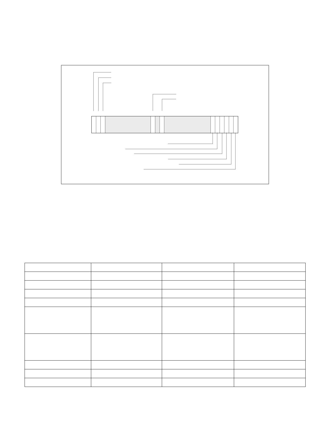
PROCESSOR MANAGEMENT AND INITIALIZATION
10.1.1 Processor State After Reset
Following power-up, The state of control register CR0 is 60000010H (see Figure 10-1). This places the processor is
in real-address mode with paging disabled.
Paging disabled: 0
Caching disabled: 1
Not write-through disabled: 1
Alignment check disabled: 0
Write-protect disabled: 0
31
30 29 28
19
18 17
16 15
6
5
4
3
2
1
0
P
C
N
A
W
N
T
E
M
P
Reserved
Reserved
1
G
D
W
M
P
E
S
M
P
E
External x87 FPU error reporting: 0
(Not used): 1
No task switch: 0
x87 FPU instructions not trapped: 0
WAIT/FWAIT instructions not trapped: 0
Real-address mode: 0
Figure 10-1. Contents of CR0 Register after Reset
The state of the flags and other registers following power-up for the Pentium 4, Pentium Pro, and Pentium proces-
sors are shown in Section 23.39, “Initial State of Pentium, Pentium Pro and Pentium 4 Processors,” of the Intel® 64
and IA-32 Architectures Software Developer’s Manual, Volume 3B.
Table 10-1 shows processor states of IA-32 and Intel 64 processors with CPUID DisplayFamily signature of 06H at
the following events: power-up, RESET, and INIT. In a few cases, the behavior of some registers behave slightly
different across warm RESET, the variant cases are marked in Table 10-1 and described in more detail in Table
10-2.
Table 10-1. IA-32 and Intel® 64 Processor States Following Power-up, Reset, or INIT
Register
Power up
Reset
INIT
EFLAGS1
00000002H
00000002H
00000002H
EIP
0000FFF0H
0000FFF0H
0000FFF0H
CR0
60000010H2
60000010H2
60000010H2
CR2, CR3, CR4
00000000H
00000000H
00000000H
CS
Selector = F000H
Selector = F000H
Selector = F000H
Base = FFFF0000H
Base = FFFF0000H
Base = FFFF0000H
Limit = FFFFH
Limit = FFFFH
Limit = FFFFH
AR = Present, R/W, Accessed
AR = Present, R/W, Accessed
AR = Present, R/W, Accessed
SS, DS, ES, FS, GS
Selector = 0000H
Selector = 0000H
Selector = 0000H
Base = 00000000H
Base = 00000000H
Base = 00000000H
Limit = FFFFH
Limit = FFFFH
Limit = FFFFH
AR = Present, R/W, Accessed
AR = Present, R/W, Accessed
AR = Present, R/W, Accessed
EDX
000n06xxH3
000n06xxH3
000n06xxH3
EAX
04
04
04
EBX, ECX, ESI, EDI, EBP, ESP
00000000H
00000000H
00000000H
10-2
Vol. 3A

PROCESSOR MANAGEMENT AND INITIALIZATION
Table 10-1. IA-32 and Intel® 64 Processor States Following Power-up, Reset, or INIT (Contd.)
Register
Power up
Reset
INIT
ST0 through ST75
+0.0
+0.0
FINIT/FNINIT: Unchanged
x87 FPU Control Word5
0040H
0040H
FINIT/FNINIT: 037FH
x87 FPU Status Word5
0000H
0000H
FINIT/FNINIT: 0000H
x87 FPU Tag Word5
5555H
5555H
FINIT/FNINIT: FFFFH
x87 FPU Data Operand and
0000H
0000H
FINIT/FNINIT: 0000H
CS Seg. Selectors5
x87 FPU Data Operand and
00000000H
00000000H
FINIT/FNINIT: 00000000H
Inst. Pointers5
MM0 through MM75
0000000000000000H
0000000000000000H
INIT or FINIT/FNINIT: Unchanged
XMM0 through XMM7
0H
0H
Unchanged
MXCSR
1F80H
1F80H
Unchanged
GDTR, IDTR
Base = 00000000H
Base = 00000000H
Base = 00000000H
Limit = FFFFH
Limit = FFFFH
Limit = FFFFH
AR = Present, R/W
AR = Present, R/W
AR = Present, R/W
LDTR, Task Register
Selector = 0000H
Selector = 0000H
Selector = 0000H
Base = 00000000H
Base = 00000000H
Base = 00000000H
Limit = FFFFH
Limit = FFFFH
Limit = FFFFH
AR = Present, R/W
AR = Present, R/W
AR = Present, R/W
DR0, DR1, DR2, DR3
00000000H
00000000H
00000000H
DR6
FFFF0FF0H
FFFF0FF0H
FFFF0FF0H
DR7
00000400H
00000400H
00000400H
R8-R15
0000000000000000H
0000000000000000H
0000000000000000H
XMM8-XMM15
0H
0H
Unchanged
XCR0
1H
1H
Unchanged
IA32_XSS
0H
0H
Unchanged
YMM_H[255:128]
0H
0H
Unchanged
BNDCFGU
0H
0H
0H
BND0-BND3
0H
0H
0H
IA32_BNDCFGS
0H
0H
0H
OPMASK
0H
0H
Unchanged
ZMM_H[511:256]
0H
0H
Unchanged
ZMMHi16[511:0]
0H
0H
Unchanged
PKRU
0H
0H
Unchanged
Intel Processor Trace MSRs
0H
0HW
Unchanged
Time-Stamp Counter
0H
0HW
Unchanged
IA32_TSC_AUX
0H
0H
Unchanged
IA32_TSC_ADJUST
0H
0H
Unchanged
IA32_TSC_DEADLINE
0H
0H
Unchanged
IA32_SYSENTER_CS/ESP/EIP
0H
0H
Unchanged
IA32_EFER
0000000000000000H
0000000000000000H
0000000000000000H
IA32_STAR/LSTAR
0H
0H
Unchanged
Vol. 3A
10-3

PROCESSOR MANAGEMENT AND INITIALIZATION
Table 10-1. IA-32 and Intel® 64 Processor States Following Power-up, Reset, or INIT (Contd.)
Register
Power up
Reset
INIT
IA32_FS_BASE/GS_BASE
0H
0H
0H
IA32_PMCx,
0H
0H
Unchanged
IA32_PERFEVTSELx
IA32_PERF_GLOBAL_CTRL
Sets bits n-1:0 and clears the
Sets bits n-1:0 and clears the
Unchanged
upper bits.7
upper bits.7
IA32_FIXED_CTRx,
0H
0H
Unchanged
IA32_FIXED_CTR_CTRL
Data and Code Cache, TLBs
Invalid6
Invalid6
Unchanged
Fixed MTRRs
Disabled
Disabled
Unchanged
Variable MTRRs
Disabled
Disabled
Unchanged
Machine-Check Banks
Undefined
UndefinedW
Unchanged
Last Branch Record Stack
0
0W
Unchanged
APIC
Enabled
Enabled
Unchanged
X2APIC
Disabled
Disabled
Unchanged
IA32_DEBUG_INTERFACE
0
0W
Unchanged
NOTES:
1. The 10 most-significant bits of the EFLAGS register are undefined following a reset. Software should not depend on the states of
any of these bits.
2. The CD and NW flags are unchanged, bit 4 is set to 1, all other bits are cleared.
3. Where “n” is the Extended Model Value for the respective processor, and “xx” = don’t care.
4. If Built-In Self-Test (BIST) is invoked on power up or reset, EAX is 0 only if all tests passed. (BIST cannot be invoked during an INIT.)
5. The state of the x87 FPU and MMX registers is not changed by the execution of an INIT.
6. Internal caches are invalid after power-up and RESET, but left unchanged with an INIT.
7. Where “n” is the number of general-purpose counters available in the processor. See Chapter 20, “Performance Monitoring,” for addi-
tional details.
W: Warm RESET behavior differs from power-on RESET with details listed in Table 10-2.
Table 10-2. Variance of RESET Values in Selected Intel Architecture Processors
State
XREF
Value
Feature Flag or DisplayFamily_DisplayModel Signatures
Time-Stamp Counter
Warm RESET
Unmodified across warm
06_2DH, 06_3EH
Reset
Machine-Check Banks
Warm RESET
IA32_MCi_Status banks are
06_2DH, 06_3EH, 06_3FH, 06_4FH, 06_56H
unmodified across warm
Reset
Last Branch Record Stack
Warm RESET
LBR stack MSRs are
06_1AH, 06_1CH, DisplayFamiy= 06 and DisplayModel >1DH
unmodified across warm
Reset
Intel Processor Trace
Warm RESET
Clears
If CPUID.(EAX=14H, ECX=0H):EBX[bit 2] = 1
MSRs
IA32_RTIT_CTL.TraceEn,
the rest of MSRs are
unmodified
IA32_DEBUG_INTERFACE
Warm RESET
Unmodified across warm
If CPUID.01H:ECX.[11] = 1
Reset
10-4
Vol. 3A
PROCESSOR MANAGEMENT AND INITIALIZATION
10.1.2 Processor Built-In Self-Test (BIST)
Hardware may request that the BIST be performed at power-up. The EAX register is cleared (0H) if the processor
passes the BIST. A nonzero value in the EAX register after the BIST indicates that a processor fault was detected.
If the BIST is not requested, the contents of the EAX register after a hardware reset is 0H.
The overhead for performing a BIST varies between processor families. For example, the BIST takes approximately
30 million processor clock periods to execute on the Pentium 4 processor. This clock count is model-specific; Intel
reserves the right to change the number of periods for any Intel 64 or IA-32 processor, without notification.
10.1.3 Model and Stepping Information
Following a hardware reset, the EDX register contains component identification and revision information (see
Figure 10-2). For example, the model, family, and processor type returned for the first processor in the Intel
Pentium 4 family is as follows: model (0000B), family (1111B), and processor type (00B).
31
28 27
20 19
1615
14 13
12 11
8 7
43
0
Extended
Extended
Stepping
EDX
Family
Model
Family
Model
ID
Processor Type
Family (1111B for the Pentium 4 Processor Family)
Model (Beginning with 0000B)
Reserved
Figure 10-2. Version Information in the EDX Register after Reset
The stepping ID field contains a unique identifier for the processor’s stepping ID or revision level. The extended
family and extended model fields were added to the IA-32 architecture in the Pentium 4 processors.
10.1.4 First Instruction Executed
The first instruction that is fetched and executed following a hardware reset is located at physical address
FFFFFFF0H. This address is 16 bytes below the processor’s uppermost physical address. The EPROM containing the
software-initialization code must be located at this address.
The address FFFFFFF0H is beyond the 1-MByte addressable range of the processor while in real-address mode. The
processor is initialized to this starting address as follows. The CS register has two parts: the visible segment
selector part and the hidden base address part. In real-address mode, the base address is normally formed by
shifting the 16-bit segment selector value 4 bits to the left to produce a 20-bit base address. However, during a
hardware reset, the segment selector in the CS register is loaded with F000H and the base address is loaded with
FFFF0000H. The starting address is thus formed by adding the base address to the value in the EIP register (that
is, FFFF0000 + FFF0H = FFFFFFF0H).
The first time the CS register is loaded with a new value after a hardware reset, the processor will follow the normal
rule for address translation in real-address mode (that is, [CS base address = CS segment selector * 16]). To
ensure that the base address in the CS register remains unchanged until the EPROM based software-initialization
code is completed, the code must not contain a far jump or far call or allow an interrupt to occur (which would
cause the CS selector value to be changed).
10.2
X87 FPU INITIALIZATION
Software-initialization code can determine the whether the processor contains an x87 FPU by using the CPUID
instruction. The code must then initialize the x87 FPU and set flags in control register CR0 to reflect the state of the
x87 FPU environment.
Vol. 3A
10-5
PROCESSOR MANAGEMENT AND INITIALIZATION
A hardware reset places the x87 FPU in the state shown in Table 10-1. This state is different from the state the x87
FPU is placed in following the execution of an FINIT or FNINIT instruction (also shown in Table 10-1). If the x87 FPU
is to be used, the software-initialization code should execute an FINIT/FNINIT instruction following a hardware
reset. These instructions, tag all data registers as empty, clear all the exception masks, set the TOP-of-stack value
to 0, and select the default rounding and precision controls setting (round to nearest and 64-bit precision).
If the processor is reset by asserting the INIT# pin, the x87 FPU state is not changed.
10.2.1 Configuring the x87 FPU Environment
Initialization code must load the appropriate values into the MP, EM, and NE flags of control register CR0. These bits
are cleared on hardware reset of the processor. Figure 10-3 shows the suggested settings for these flags,
depending on the IA-32 processor being initialized. Initialization code can test for the type of processor present
before setting or clearing these flags.
Table 10-3. Recommended Settings of EM and MP Flags on IA-32 Processors
EM
MP
NE
IA-32 processor
1
0
1
Intel486™ SX, Intel386™ DX, and Intel386™ SX processors only, without the presence of a math
coprocessor.
0
1
1 or 0*
Pentium 4, Intel Xeon, P6 family, Pentium, Intel486™ DX, and Intel 487 SX processors, and
Intel386 DX and Intel386 SX processors when a companion math coprocessor is present.
0
1
1 or 0*
More recent Intel 64 or IA-32 processors
NOTE:
* The setting of the NE flag depends on the operating system being used.
The EM flag determines whether floating-point instructions are executed by the x87 FPU (EM is cleared) or a
device-not-available exception (#NM) is generated for all floating-point instructions so that an exception handler
can emulate the floating-point operation (EM = 1). Ordinarily, the EM flag is cleared when an x87 FPU or math
coprocessor is present and set if they are not present. If the EM flag is set and no x87 FPU, math coprocessor, or
floating-point emulator is present, the processor will hang when a floating-point instruction is executed.
The MP flag determines whether WAIT/FWAIT instructions react to the setting of the TS flag. If the MP flag is clear,
WAIT/FWAIT instructions ignore the setting of the TS flag; if the MP flag is set, they will generate a device-not-
available exception (#NM) if the TS flag is set. Generally, the MP flag should be set for processors with an inte-
grated x87 FPU and clear for processors without an integrated x87 FPU and without a math coprocessor present.
However, an operating system can choose to save the floating-point context at every context switch, in which case
there would be no need to set the MP bit.
Table 2-2 shows the actions taken for floating-point and WAIT/FWAIT instructions based on the settings of the EM,
MP, and TS flags.
The NE flag determines whether unmasked floating-point exceptions are handled by generating a floating-point
error exception internally (NE is set, native mode) or through an external interrupt (NE is cleared). In systems
where an external interrupt controller is used to invoke numeric exception handlers (such as MS-DOS-based
systems), the NE bit should be cleared.
10.2.2 Setting the Processor for x87 FPU Software Emulation
Setting the EM flag causes the processor to generate a device-not-available exception (#NM) and trap to a software
exception handler whenever it encounters a floating-point instruction. (Table 10-3 shows when it is appropriate to
use this flag.) Setting this flag has two functions:
• It allows x87 FPU code to run on an IA-32 processor that has neither an integrated x87 FPU nor is connected to
an external math coprocessor, by using a floating-point emulator.
• It allows floating-point code to be executed using a special or nonstandard floating-point emulator, selected for
a particular application, regardless of whether an x87 FPU or math coprocessor is present.
10-6
Vol. 3A
PROCESSOR MANAGEMENT AND INITIALIZATION
To emulate floating-point instructions, the EM, MP, and NE flag in control register CR0 should be set as shown in
Table 10-4.
Table 10-4. Software Emulation Settings of EM, MP, and NE Flags
CR0 Bit
Value
EM
1
MP
0
NE
1
Regardless of the value of the EM bit, the Intel486 SX processor generates a device-not-available exception (#NM)
upon encountering any floating-point instruction.
10.3
CACHE ENABLING
IA-32 processors (beginning with the Intel486 processor) and Intel 64 processors contain internal instruction and
data caches. These caches are enabled by clearing the CD and NW flags in control register CR0. (They are set
during a hardware reset.) Because all internal cache lines are invalid following reset initialization, it is not neces-
sary to invalidate the cache before enabling caching. Any external caches may require initialization and invalidation
using a system-specific initialization and invalidation code sequence.
Depending on the hardware and operating system or executive requirements, additional configuration of the
processor’s caching facilities will probably be required. Beginning with the Intel486 processor, page-level caching
can be controlled with the PCD and PWT flags in page-directory and page-table entries. Beginning with the P6
family processors, the memory type range registers (MTRRs) control the caching characteristics of the regions of
physical memory. (For the Intel486 and Pentium processors, external hardware can be used to control the caching
characteristics of regions of physical memory.) See Chapter 12, “Memory Cache Control,” for detailed information
on configuration of the caching facilities in the Pentium 4, Intel Xeon, and P6 family processors and system
memory.
10.4
MODEL-SPECIFIC REGISTERS (MSRS)
Most IA-32 processors (starting from Pentium processors) and Intel 64 processors contain a model-specific regis-
ters (MSRs). A given MSR may not be supported across all families and models for Intel 64 and IA-32 processors.
Some MSRs are designated as architectural to simplify software programming; a feature introduced by an architec-
tural MSR is expected to be supported in future processors. Non-architectural MSRs are not guaranteed to be
supported or to have the same functions on future processors.
MSRs that provide control for a number of hardware and software-related features, include:
• Performance-monitoring counters (see Chapter 20, “Performance Monitoring”).
• Debug extensions (see Chapter 18, “Debug, Branch Profile, TSC, and Intel® Resource Director Technology
(Intel® RDT) Features”).
• Machine-check exception capability and its accompanying machine-check architecture (see Chapter 16,
“Machine-Check Architecture”).
• MTRRs (see Section 12.11, “Memory Type Range Registers (MTRRs)”).
• Thermal and power management.
• Instruction-specific support (for example: SYSENTER, SYSEXIT, SWAPGS, etc.).
• Processor feature/mode support (for example: IA32_EFER, IA32_FEATURE_CONTROL).
The MSRs can be read and written to using the RDMSR and WRMSR instructions, respectively.
When performing software initialization of an IA-32 or Intel 64 processor, many of the MSRs will need to be initial-
ized to set up things like performance-monitoring events, run-time machine checks, and memory types for phys-
ical memory.
Vol. 3A
10-7
PROCESSOR MANAGEMENT AND INITIALIZATION
Lists of available performance-monitoring events can be found at: https://perfmon-events.intel.com/ , and lists of
available MSRs are given in Chapter 2, “Model-Specific Registers (MSRs)‚” in the Intel® 64 and IA-32 Architectures
Software Developer’s Manual, Volume 4. The references earlier in this section show where the functions of the
various groups of MSRs are described in this manual.
10.5
MEMORY TYPE RANGE REGISTERS (MTRRS)
Memory type range registers (MTRRs) were introduced into the IA-32 architecture with the Pentium Pro processor.
They allow the type of caching (or no caching) to be specified in system memory for selected physical address
ranges. They allow memory accesses to be optimized for various types of memory such as RAM, ROM, frame buffer
memory, and memory-mapped I/O devices.
In general, initializing the MTRRs is normally handled by the software initialization code or BIOS and is not an oper-
ating system or executive function. At the very least, all the MTRRs must be cleared to 0, which selects the
uncached (UC) memory type. See Section 12.11, “Memory Type Range Registers (MTRRs),” for detailed informa-
tion on the MTRRs.
10.6
INITIALIZING SSE/SSE2/SSE3/SSSE3 EXTENSIONS
For processors that contain SSE/SSE2/SSE3/SSSE3 extensions, steps must be taken when initializing the
processor to allow execution of these instructions.
1. Check the CPUID feature flags for the presence of the SSE/SSE2/SSE3/SSSE3 extensions (respectively: EDX
bits 25 and 26, ECX bit 0 and 9) and support for the FXSAVE and FXRSTOR instructions (EDX bit 24). Also check
for support for the CLFLUSH instruction (EDX bit 19). The CPUID feature flags are loaded in the EDX and ECX
registers when the CPUID instruction is executed with a 1 in the EAX register.
2. Set the OSFXSR flag (bit 9 in control register CR4) to indicate that the operating system supports saving and
restoring the SSE/SSE2/SSE3/SSSE3 execution environment (XMM and MXCSR registers) with the FXSAVE and
FXRSTOR instructions, respectively. See Section 2.5, “Control Registers,” for a description of the OSFXSR flag.
3. Set the OSXMMEXCPT flag (bit 10 in control register CR4) to indicate that the operating system supports the
handling of SSE/SSE2/SSE3 SIMD floating-point exceptions (#XM). See Section 2.5, “Control Registers,” for a
description of the OSXMMEXCPT flag.
4. Set the mask bits and flags in the MXCSR register according to the mode of operation desired for
SSE/SSE2/SSE3 SIMD floating-point instructions. See “MXCSR Control and Status Register” in Chapter 10,
“Programming with Intel® Streaming SIMD Extensions (Intel® SSE),” of the Intel® 64 and IA-32 Architectures
Software Developer’s Manual, Volume 1, for a detailed description of the bits and flags in the MXCSR register.
10.7
SOFTWARE INITIALIZATION FOR REAL-ADDRESS MODE OPERATION
Following a hardware reset (either through a power-up or the assertion of the RESET# pin) the processor is placed
in real-address mode and begins executing software initialization code from physical address FFFFFFF0H. Software
initialization code must first set up the necessary data structures for handling basic system functions, such as a
real-mode IDT for handling interrupts and exceptions. If the processor is to remain in real-address mode, software
must then load additional operating-system or executive code modules and data structures to allow reliable execu-
tion of application programs in real-address mode.
If the processor is going to operate in protected mode, software must load the necessary data structures to operate
in protected mode and then switch to protected mode. The protected-mode data structures that must be loaded
are described in Section 10.8, “Software Initialization for Protected-Mode Operation.”
10.7.1 Real-Address Mode IDT
In real-address mode, the only system data structure that must be loaded into memory is the IDT (also called the
“interrupt vector table”). By default, the address of the base of the IDT is physical address 0H. This address can be
10-8
Vol. 3A
PROCESSOR MANAGEMENT AND INITIALIZATION
changed by using the LIDT instruction to change the base address value in the IDTR. Software initialization code
needs to load interrupt- and exception-handler pointers into the IDT before interrupts can be enabled.
The actual interrupt- and exception-handler code can be contained either in EPROM or RAM; however, the code
must be located within the 1-MByte addressable range of the processor in real-address mode. If the handler code
is to be stored in RAM, it must be loaded along with the IDT.
10.7.2 NMI Interrupt Handling
The NMI interrupt is always enabled (except when multiple NMIs are nested). If the IDT and the NMI interrupt
handler need to be loaded into RAM, there will be a period of time following hardware reset when an NMI interrupt
cannot be handled. During this time, hardware must provide a mechanism to prevent an NMI interrupt from halting
code execution until the IDT and the necessary NMI handler software is loaded. Here are two examples of how
NMIs can be handled during the initial states of processor initialization:
• A simple IDT and NMI interrupt handler can be provided in EPROM. This allows an NMI interrupt to be handled
immediately after reset initialization.
• The system hardware can provide a mechanism to enable and disable NMIs by passing the NMI# signal through
an AND gate controlled by a flag in an I/O port. Hardware can clear the flag when the processor is reset, and
software can set the flag when it is ready to handle NMI interrupts.
10.8
SOFTWARE INITIALIZATION FOR PROTECTED-MODE OPERATION
The processor is placed in real-address mode following a hardware reset. At this point in the initialization process,
some basic data structures and code modules must be loaded into physical memory to support further initialization
of the processor, as described in Section 10.7, “Software Initialization for Real-Address Mode Operation.” Before
the processor can be switched to protected mode, the software initialization code must load a minimum number of
protected mode data structures and code modules into memory to support reliable operation of the processor in
protected mode. These data structures include the following:
• A IDT.
• A GDT.
• A TSS.
• (Optional) An LDT.
• If paging is to be used, at least one page directory and one page table.
• A code segment that contains the code to be executed when the processor switches to protected mode.
• One or more code modules that contain the necessary interrupt and exception handlers.
Software initialization code must also initialize the following system registers before the processor can be switched
to protected mode:
• The GDTR.
• (Optional.) The IDTR. This register can also be initialized immediately after switching to protected mode, prior
to enabling interrupts.
• Control registers CR1 through CR4.
• (Pentium 4, Intel Xeon, and P6 family processors only.) The memory type range registers (MTRRs).
With these data structures, code modules, and system registers initialized, the processor can be switched to
protected mode by loading control register CR0 with a value that sets the PE flag (bit 0).
10.8.1 Protected-Mode System Data Structures
The contents of the protected-mode system data structures loaded into memory during software initialization,
depend largely on the type of memory management the protected-mode operating-system or executive is going to
support: flat, flat with paging, segmented, or segmented with paging.
Vol. 3A
10-9
PROCESSOR MANAGEMENT AND INITIALIZATION
To implement a flat memory model without paging, software initialization code must at a minimum load a GDT with
one code and one data-segment descriptor. A null descriptor in the first GDT entry is also required. The stack can
be placed in a normal read/write data segment, so no dedicated descriptor for the stack is required. A flat memory
model with paging also requires a page directory and at least one page table (unless all pages are 4 MBytes in
which case only a page directory is required). See Section 10.8.3, “Initializing Paging.”
Before the GDT can be used, the base address and limit for the GDT must be loaded into the GDTR register using
an LGDT instruction.
A multi-segmented model may require additional segments for the operating system, as well as segments and LDTs
for each application program. LDTs require segment descriptors in the GDT. Some operating systems allocate new
segments and LDTs as they are needed. This provides maximum flexibility for handling a dynamic programming
environment. However, many operating systems use a single LDT for all tasks, allocating GDT entries in advance.
An embedded system, such as a process controller, might pre-allocate a fixed number of segments and LDTs for a
fixed number of application programs. This would be a simple and efficient way to structure the software environ-
ment of a real-time system.
10.8.2 Initializing Protected-Mode Exceptions and Interrupts
Software initialization code must at a minimum load a protected-mode IDT with gate descriptor for each exception
vector that the processor can generate. If interrupt or trap gates are used, the gate descriptors can all point to the
same code segment, which contains the necessary exception handlers. If task gates are used, one TSS and accom-
panying code, data, and task segments are required for each exception handler called with a task gate.
If hardware allows interrupts to be generated, gate descriptors must be provided in the IDT for one or more inter-
rupt handlers.
Before the IDT can be used, the base address and limit for the IDT must be loaded into the IDTR register using an
LIDT instruction. This operation is typically carried out immediately after switching to protected mode.
10.8.3 Initializing Paging
Paging is controlled by the PG flag in control register CR0. When this flag is clear (its state following a hardware
reset), the paging mechanism is turned off; when it is set, paging is enabled. Before setting the PG flag, the
following data structures and registers must be initialized:
• Software must load at least one page directory and one page table into physical memory. The page table can
be eliminated if the page directory contains a directory entry pointing to itself (here, the page directory and
page table reside in the same page), or if only 4-MByte pages are used.
• Control register CR3 (also called the PDBR register) is loaded with the physical base address of the page
directory.
• (Optional) Software may provide one set of code and data descriptors in the GDT or in an LDT for supervisor
mode and another set for user mode.
With this paging initialization complete, paging is enabled and the processor is switched to protected mode at the
same time by loading control register CR0 with an image in which the PG and PE flags are set. (Paging cannot be
enabled before the processor is switched to protected mode.)
10.8.4 Initializing Multitasking
If the multitasking mechanism is not going to be used and changes between privilege levels are not allowed, it is
not necessary load a TSS into memory or to initialize the task register.
If the multitasking mechanism is going to be used and/or changes between privilege levels are allowed, software
initialization code must load at least one TSS and an accompanying TSS descriptor. (A TSS is required to change
privilege levels because pointers to the privileged-level 0, 1, and 2 stack segments and the stack pointers for these
stacks are obtained from the TSS.) TSS descriptors must not be marked as busy when they are created; they
should be marked busy by the processor only as a side-effect of performing a task switch. As with descriptors for
LDTs, TSS descriptors reside in the GDT.
10-10
Vol. 3A
PROCESSOR MANAGEMENT AND INITIALIZATION
After the processor has switched to protected mode, the LTR instruction can be used to load a segment selector for
a TSS descriptor into the task register. This instruction marks the TSS descriptor as busy, but does not perform a
task switch. The processor can, however, use the TSS to locate pointers to privilege-level 0, 1, and 2 stacks. The
segment selector for the TSS must be loaded before software performs its first task switch in protected mode,
because a task switch copies the current task state into the TSS.
After the LTR instruction has been executed, further operations on the task register are performed by task
switching. As with other segments and LDTs, TSSs and TSS descriptors can be either pre-allocated or allocated as
needed.
10.8.5 Initializing IA-32e Mode
On Intel 64 processors, the IA32_EFER MSR is cleared on system reset. The operating system must be in protected
mode with paging enabled before attempting to initialize IA-32e mode. IA-32e mode operation also requires phys-
ical-address extensions with four or five levels of enhanced paging structures (see Section 4.5, “4-Level Paging and
5-Level Paging”).
Operating systems should follow this sequence to initialize IA-32e mode:
1. Starting from protected mode, disable paging by setting CR0.PG = 0. Use the MOV CR0 instruction to disable
paging (the instruction must be located in an identity-mapped page).
2. Enable physical-address extensions (PAE) by setting CR4.PAE = 1. Failure to enable PAE will result in a #GP
fault when an attempt is made to initialize IA-32e mode.
3. Load CR3 with the physical base address of the Level 4 page map table (PML4) or Level 5 page map table
(PML5).
4. Enable IA-32e mode by setting IA32_EFER.LME = 1.
5. Enable paging by setting CR0.PG = 1. This causes the processor to set the IA32_EFER.LMA bit to 1. The MOV
CR0 instruction that enables paging and the following instructions must be located in an identity-mapped page
(until such time that a branch to non-identity mapped pages can be effected).
64-bit mode paging structures must be located in the first 4 GBytes of physical-address space prior to activating
IA-32e mode. This is necessary because the MOV CR3 instruction used to initialize the page-directory base must be
executed in legacy mode prior to activating IA-32e mode (setting CR0.PG = 1 to enable paging). Because MOV CR3
is executed in protected mode, only the lower 32 bits of the register are written, limiting the table location to the
low 4 GBytes of memory. Software can relocate the page tables anywhere in physical memory after IA-32e mode
is activated.
The processor performs 64-bit mode consistency checks whenever software attempts to modify any of the enable
bits directly involved in activating IA-32e mode (IA32_EFER.LME, CR0.PG, and CR4.PAE). It will generate a general
protection fault (#GP) if consistency checks fail. 64-bit mode consistency checks ensure that the processor does
not enter an undefined mode or state with unpredictable behavior.
64-bit mode consistency checks fail in the following circumstances:
• An attempt is made to enable or disable IA-32e mode while paging is enabled.
• IA-32e mode is enabled and an attempt is made to enable paging prior to enabling physical-address extensions
(PAE).
• IA-32e mode is active and an attempt is made to disable physical-address extensions (PAE).
• If the current CS has the L-bit set on an attempt to activate IA-32e mode.
• If the TR contains a 16-bit TSS on an attempt to activate IA-32e mode.
10.8.5.1 IA-32e Mode System Data Structures
After activating IA-32e mode, the system-descriptor-table registers (GDTR, LDTR, IDTR, TR) continue to reference
legacy protected-mode descriptor tables. Tables referenced by the descriptors all reside in the lower 4 GBytes of
linear-address space. After activating IA-32e mode, 64-bit operating-systems should use the LGDT, LLDT, LIDT,
and LTR instructions to load the system-descriptor-table registers with references to 64-bit descriptor tables.
Vol. 3A
10-11
PROCESSOR MANAGEMENT AND INITIALIZATION
10.8.5.2 IA-32e Mode Interrupts and Exceptions
Software must not allow exceptions or interrupts to occur between the time IA-32e mode is activated and the
update of the interrupt-descriptor-table register (IDTR) that establishes references to a 64-bit interrupt-descriptor
table (IDT). This is because the IDT remains in legacy form immediately after IA-32e mode is activated.
If an interrupt or exception occurs prior to updating the IDTR, a legacy 32-bit interrupt gate will be referenced and
interpreted as a 64-bit interrupt gate with unpredictable results. External interrupts can be disabled by using the
CLI instruction.
Non-maskable interrupts (NMI) must be disabled using external hardware.
10.8.5.3
64-bit Mode and Compatibility Mode Operation
IA-32e mode uses two code segment-descriptor bits (CS.L and CS.D, see Figure 3-8) to control the operating modes
after IA-32e mode is initialized. If CS.L = 1 and CS.D = 0, the processor is running in 64-bit mode. With this
encoding, the default operand size is 32 bits and default address size is 64 bits. Using instruction prefixes, operand
size can be changed to 64 bits or 16 bits; address size can be changed to 32 bits.
When IA-32e mode is active and CS.L = 0, the processor operates in compatibility mode. In this mode, CS.D
controls default operand and address sizes exactly as it does in the IA-32 architecture. Setting CS.D = 1 specifies
default operand and address size as 32 bits. Clearing CS.D to 0 specifies default operand and address size as 16
bits (the CS.L = 1, CS.D = 1 bit combination is reserved).
Compatibility mode execution is selected on a code-segment basis. This mode allows legacy applications to coexist
with 64-bit applications running in 64-bit mode. An operating system running in IA-32e mode can execute existing
16-bit and 32-bit applications by clearing their code-segment descriptor’s CS.L bit to 0.
In compatibility mode, the following system-level mechanisms continue to operate using the IA-32e-mode archi-
tectural semantics:
• Linear-to-physical address translation uses the 64-bit mode extended page-translation mechanism.
• Interrupts and exceptions are handled using the 64-bit mode mechanisms.
• System calls (calls through call gates and SYSENTER/SYSEXIT) are handled using the IA-32e mode
mechanisms.
10.8.5.4 Switching Out of IA-32e Mode Operation
To return from IA-32e mode to paged-protected mode operation operating systems must use the following
sequence:
1. Switch to compatibility mode.
2. Deactivate IA-32e mode by clearing CR0.PG = 0. This causes the processor to set IA32_EFER.LMA = 0. The
MOV CR0 instruction used to disable paging and subsequent instructions must be located in an identity-mapped
page.
3. Load CR3 with the physical base address of the legacy page-table-directory base address.
4. Disable IA-32e mode by setting IA32_EFER.LME = 0.
5. Enable legacy paged-protected mode by setting CR0.PG = 1
6. A branch instruction must follow the MOV CR0 that enables paging. Both the MOV CR0 and the branch
instruction must be located in an identity-mapped page.
Registers only available in 64-bit mode (R8-R15 and XMM8-XMM15) are preserved across transitions from 64-bit
mode into compatibility mode then back into 64-bit mode. However, values of R8-R15 and XMM8-XMM15 are unde-
fined after transitions from 64-bit mode through compatibility mode to legacy or real mode and then back through
compatibility mode to 64-bit mode.
10-12
Vol. 3A
PROCESSOR MANAGEMENT AND INITIALIZATION
10.9
MODE SWITCHING
To use the processor in protected mode after hardware or software reset, a mode switch must be performed from
real-address mode. Once in protected mode, software generally does not need to return to real-address mode. To
run software written to run in real-address mode (8086 mode), it is generally more convenient to run the software
in virtual-8086 mode, than to switch back to real-address mode.
10.9.1 Switching to Protected Mode
Before switching to protected mode from real mode, a minimum set of system data structures and code modules
must be loaded into memory, as described in Section 10.8, “Software Initialization for Protected-Mode Operation.”
Once these tables are created, software initialization code can switch into protected mode.
Protected mode is entered by executing a MOV CR0 instruction that sets the PE flag in the CR0 register. (In the
same instruction, the PG flag in register CR0 can be set to enable paging.) Execution in protected mode begins with
a CPL of 0.
Intel 64 and IA-32 processors have slightly different requirements for switching to protected mode. To ensure
upwards and downwards code compatibility with Intel 64 and IA-32 processors, we recommend that you follow
these steps:
1. Disable interrupts. A CLI instruction disables maskable hardware interrupts. NMI interrupts can be disabled
with external circuitry. (Software must guarantee that no exceptions or interrupts are generated during the
mode switching operation.)
2. Execute the LGDT instruction to load the GDTR register with the base address of the GDT.
3. Execute a MOV CR0 instruction that sets the PE flag (and optionally the PG flag) in control register CR0.
4. Immediately following the MOV CR0 instruction, execute a far JMP or far CALL instruction. (This operation is
typically a far jump or call to the next instruction in the instruction stream.)
5. The JMP or CALL instruction immediately after the MOV CR0 instruction changes the flow of execution and
serializes the processor.
6. If paging is enabled, the code for the MOV CR0 instruction and the JMP or CALL instruction must come from a
page that is identity mapped (that is, the linear address before the jump is the same as the physical address
after paging and protected mode is enabled). The target instruction for the JMP or CALL instruction does not
need to be identity mapped.
7. If a local descriptor table is going to be used, execute the LLDT instruction to load the segment selector for the
LDT in the LDTR register.
8. Execute the LTR instruction to load the task register with a segment selector to the initial protected-mode task
or to a writable area of memory that can be used to store TSS information on a task switch.
9. After entering protected mode, the segment registers continue to hold the contents they had in real-address
mode. The JMP or CALL instruction in step 4 resets the CS register. Perform one of the following operations to
update the contents of the remaining segment registers.
- Reload segment registers DS, SS, ES, FS, and GS. If the ES, FS, and/or GS registers are not going to be
used, load them with a null selector.
- Perform a JMP or CALL instruction to a new task, which automatically resets the values of the segment
registers and branches to a new code segment.
10. Execute the LIDT instruction to load the IDTR register with the address and limit of the protected-mode IDT.
11. Execute the STI instruction to enable maskable hardware interrupts and perform the necessary hardware
operation to enable NMI interrupts.
Random failures can occur if other instructions exist between steps 3 and 4 above. Failures will be readily seen in
some situations, such as when instructions that reference memory are inserted between steps 3 and 4 while in
system management mode.
Vol. 3A
10-13
PROCESSOR MANAGEMENT AND INITIALIZATION
10.9.2 Switching Back to Real-Address Mode
The processor switches from protected mode back to real-address mode if software clears the PE bit in the CR0
register with a MOV CR0 instruction. A procedure that re-enters real-address mode should perform the following
steps:
1.
Disable interrupts. A CLI instruction disables maskable hardware interrupts. NMI interrupts can be disabled
with external circuitry.
2.
If paging is enabled, perform the following operations:
- Transfer program control to linear addresses that are identity mapped to physical addresses (that is, linear
addresses equal physical addresses).
- Ensure that the GDT and IDT are in identity mapped pages.
- Clear the PG bit in the CR0 register.
- Move 0H into the CR3 register to flush the TLB.
3.
Transfer program control to a readable segment that has a limit of 64 KBytes (FFFFH). This operation loads the
CS register with the segment limit required in real-address mode.
4.
Load segment registers SS, DS, ES, FS, and GS with a selector for a descriptor containing the following values,
which are appropriate for real-address mode:
- Limit = 64 KBytes (0FFFFH)
- Byte granular (G = 0)
- Expand up (E = 0)
- Writable (W = 1)
- Present (P = 1)
- Base = any value
The segment registers must be loaded with non-null segment selectors or the segment registers will be
unusable in real-address mode. Note that if the segment registers are not reloaded, execution continues using
the descriptor attributes loaded during protected mode.
5.
Execute an LIDT instruction to point to a real-address mode interrupt table that is within the 1-MByte real-
address mode address range.
6.
Clear the PE flag in the CR0 register to switch to real-address mode.
7.
Execute a far JMP instruction to jump to a real-address mode program. This operation flushes the instruction
queue and loads the appropriate base-address value in the CS register.
8.
Load the SS, DS, ES, FS, and GS registers as needed by the real-address mode code. If any of the registers are
not going to be used in real-address mode, write 0s to them.
9.
Execute the STI instruction to enable maskable hardware interrupts and perform the necessary hardware
operation to enable NMI interrupts.
NOTE
All the code that is executed in steps 1 through 9 must be in a single page and the linear addresses
in that page must be identity mapped to physical addresses.
10.10 INITIALIZATION AND MODE SWITCHING EXAMPLE
This section provides an initialization and mode switching example that can be incorporated into an application.
This code was originally written to initialize the Intel386 processor, but it will execute successfully on the Pentium
4, Intel Xeon, P6 family, Pentium, and Intel486 processors. The code in this example is intended to reside in EPROM
and to run following a hardware reset of the processor. The function of the code is to do the following:
• Establish a basic real-address mode operating environment.
10-14
Vol. 3A
PROCESSOR MANAGEMENT AND INITIALIZATION
• Load the necessary protected-mode system data structures into RAM.
• Load the system registers with the necessary pointers to the data structures and the appropriate flag settings
for protected-mode operation.
• Switch the processor to protected mode.
Figure 10-3 shows the physical memory layout for the processor following a hardware reset and the starting point
of this example. The EPROM that contains the initialization code resides at the upper end of the processor’s physical
memory address range, starting at address FFFFFFFFH and going down from there. The address of the first instruc-
tion to be executed is at FFFFFFF0H, the default starting address for the processor following a hardware reset.
The main steps carried out in this example are summarized in Table 10-5. The source listing for the example (with
the filename STARTUP.ASM) is given in Example 10-1. The line numbers given in Table 10-5 refer to the source
listing.
The following are some additional notes concerning this example:
• When the processor is switched into protected mode, the original code segment base-address value of
FFFF0000H (located in the hidden part of the CS register) is retained and execution continues from the current
offset in the EIP register. The processor will thus continue to execute code in the EPROM until a far jump or call
is made to a new code segment, at which time, the base address in the CS register will be changed.
• Maskable hardware interrupts are disabled after a hardware reset and should remain disabled until the
necessary interrupt handlers have been installed. The NMI interrupt is not disabled following a reset. The NMI#
pin must thus be inhibited from being asserted until an NMI handler has been loaded and made available to the
processor.
• The use of a temporary GDT allows simple transfer of tables from the EPROM to anywhere in the RAM area. A
GDT entry is constructed with its base pointing to address 0 and a limit of 4 GBytes. When the DS and ES
registers are loaded with this descriptor, the temporary GDT is no longer needed and can be replaced by the
application GDT.
• This code loads one TSS and no LDTs. If more TSSs exist in the application, they must be loaded into RAM. If
there are LDTs they may be loaded as well.
After Reset
FFFF FFFFH
[CS.BASE+EIP]
FFFF FFF0H
64K EPROM
EIP = 0000 FFF0H
CS.BASE = FFFF 0000H
FFFF 0000H
DS.BASE = 0H
ES.BASE = 0H
SS.BASE = 0H
ESP = 0H
[SP, DS, SS, ES]
0
Figure 10-3. Processor State After Reset
Vol. 3A
10-15

PROCESSOR MANAGEMENT AND INITIALIZATION
Table 10-5. Main Initialization Steps in STARTUP.ASM Source Listing
STARTUP.ASM Line
Description
Numbers
From
To
157
157
Jump (short) to the entry code in the EPROM
162
169
Construct a temporary GDT in RAM with one entry:
0 - null
1 - R/W data segment, base = 0, limit = 4 GBytes
171
172
Load the GDTR to point to the temporary GDT
174
177
Load CR0 with PE flag set to switch to protected mode
179
181
Jump near to clear real mode instruction queue
184
186
Load DS, ES registers with GDT[1] descriptor, so both point to the entire physical memory space
188
195
Perform specific board initialization that is imposed by the new protected mode
196
218
Copy the application's GDT from ROM into RAM
220
238
Copy the application's IDT from ROM into RAM
241
243
Load application's GDTR
244
245
Load application's IDTR
247
261
Copy the application's TSS from ROM into RAM
263
267
Update TSS descriptor and other aliases in GDT (GDT alias or IDT alias)
277
277
Load the task register (without task switch) using LTR instruction
282
286
Load SS, ESP with the value found in the application's TSS
287
287
Push EFLAGS value found in the application's TSS
288
288
Push CS value found in the application's TSS
289
289
Push EIP value found in the application's TSS
290
293
Load DS, ES with the value found in the application's TSS
296
296
Perform IRET; pop the above values and enter the application code
10.10.1 Assembler Usage
In this example, the Intel assembler ASM386 and build tools BLD386 are used to assemble and build the initializa-
tion code module. The following assumptions are used when using the Intel ASM386 and BLD386 tools.
• The ASM386 will generate the right operand size opcodes according to the code-segment attribute. The
attribute is assigned either by the ASM386 invocation controls or in the code-segment definition.
• If a code segment that is going to run in real-address mode is defined, it must be set to a USE 16 attribute. If
a 32-bit operand is used in an instruction in this code segment (for example, MOV EAX, EBX), the assembler
automatically generates an operand prefix for the instruction that forces the processor to execute a 32-bit
operation, even though its default code-segment attribute is 16-bit.
• Intel's ASM386 assembler allows specific use of the 16- or 32-bit instructions, for example, LGDTW, LGDTD,
IRETD. If the generic instruction LGDT is used, the default- segment attribute will be used to generate the right
opcode.
10.10.2 STARTUP.ASM Listing
Example 10-1 provides high-level sample code designed to move the processor into protected mode. This listing
does not include any opcode and offset information.
10-16
Vol. 3A
PROCESSOR MANAGEMENT AND INITIALIZATION
Example 10-1. STARTUP.ASM
MS-DOS* 5.0(045-N) 386(TM) MACRO ASSEMBLER STARTUP
09:44:51 08/19/92 PAGE 1
MS-DOS 5.0(045-N) 386(TM) MACRO ASSEMBLER V4.0, ASSEMBLY OF MODULE STARTUP
OBJECT MODULE PLACED IN startup.obj
ASSEMBLER INVOKED BY: f:\386tools\ASM386.EXE startup.a58 pw (132 )
LINE
SOURCE
1
NAME
STARTUP
2
3
;;;;;;;;;;;;;;;;;;;;;;;;;;;;;;;;;;;;;;;;;;;;
4
;
5
;
ASSUMPTIONS:
6
;
7
;
1. The bottom 64K of memory is ram, and can be used for
8
;
scratch space by this module.
9
;
10
;
2. The system has sufficient free usable ram to copy the
11
;
initial GDT, IDT, and TSS
12
;
13
;;;;;;;;;;;;;;;;;;;;;;;;;;;;;;;;;;;;;;;;;;;;;;;;;;;;;;;;;;;;;;
14
15
; configuration data - must match with build definition
16
17
CS_BASE
EQU
0FFFF0000H
18
19
; CS_BASE is the linear address of the segment STARTUP_CODE
20
; - this is specified in the build language file
21
22
RAM_START
EQU
400H
23
24
; RAM_START is the start of free, usable ram in the linear
25
; memory space.
The GDT, IDT, and initial TSS will be
26
; copied above this space, and a small data segment will be
27
; discarded at this linear address.
The 32-bit word at
28
; RAM_START will contain the linear address of the first
29
; free byte above the copied tables - this may be useful if
30
; a memory manager is used.
31
32
TSS_INDEX
EQU
10
33
34
; TSS_INDEX is the index of the TSS of the first task to
35
; run after startup
36
37
38
;;;;;;;;;;;;;;;;;;;;;;;;;;;;;;;;;;;;;;;;;;;;;;;;;;;;;;;;;;;;
39
40
; ------------------------- STRUCTURES and EQU ---------------
41
; structures for system data
42
43
; TSS structure
44
TASK_STATE STRUC
45
link
DW ?
Vol. 3A
10-17
PROCESSOR MANAGEMENT AND INITIALIZATION
46
link_h
DW ?
47
ESP0
DD ?
48
SS0
DW ?
49
SS0_h
DW ?
50
ESP1
DD ?
51
SS1
DW ?
52
SS1_h
DW ?
53
ESP2
DD ?
54
SS2
DW ?
55
SS2_h
DW ?
56
CR3_reg
DD ?
57
EIP_reg
DD ?
58
EFLAGS_regDD ?
59
EAX_reg DD ?
60
ECX_reg DD ?
61
EDX_reg DD ?
62
EBX_reg DD ?
63
ESP_reg DD ?
64
EBP_reg DD ?
65
ESI_reg DD ?
66
EDI_reg DD ?
67
ES_reg
DW ?
68
ES_h
DW ?
69
CS_reg
DW ?
70
CS_h
DW ?
71
SS_reg
DW ?
72
SS_h
DW ?
73
DS_reg
DW ?
74
DS_h
DW ?
75
FS_reg
DW ?
76
FS_h
DW ?
77
GS_reg
DW ?
78
GS_h
DW ?
79
LDT_reg
DW ?
80
LDT_h
DW ?
81
TRAP_reg DW ?
82
IO_map_baseDW ?
83 TASK_STATE ENDS
84
85
; basic structure of a descriptor
86
DESC
STRUC
87
lim_0_15 DW ?
88
bas_0_15 DW ?
89
bas_16_23DB ?
90
access
DB ?
91
gran
DB ?
92
bas_24_31DB ?
93 DESC
ENDS
94
95
; structure for use with LGDT and LIDT instructions
96
TABLE_REG
STRUC
97
table_limDW ?
98
table_linearDD ?
99 TABLE_REG
ENDS
10-18
Vol. 3A