Intel 64 and IA-32 Architectures. Software Developer’s Manual (Collection, 2023) - page 43
SYSTEM ARCHITECTURE OVERVIEW
Table 14-1). If an IA-32 or Intel 64 processor incorporates the SSE/SSE2/SSE3/SSSE3/SSE4 extensions,
the EM flag must be set to 0 to enable execution of these extensions. SSE/SSE2/SSE3/SSSE3/SSE4
instructions not affected by the EM flag include: PAUSE, PREFETCHh, SFENCE, LFENCE, MFENCE, MOVNTI,
CLFLUSH, CRC32, and POPCNT.
CR0.MP
Monitor Coprocessor (bit 1 of CR0) - Controls the interaction of the WAIT (or FWAIT) instruction with
the TS flag (bit 3 of CR0). If the MP flag is set, a WAIT instruction generates a device-not-available exception
(#NM) if the TS flag is also set. If the MP flag is clear, the WAIT instruction ignores the setting of the TS flag.
Table 10-3 shows the recommended setting of this flag, depending on the IA-32 processor and x87 FPU or
math coprocessor present in the system. Table 2-2 shows the interaction of the MP, EM, and TS flags.
CR0.PE
Protection Enable (bit 0 of CR0) - Enables protected mode when set; enables real-address mode when
clear. This flag does not enable paging directly. It only enables segment-level protection. To enable paging,
both the PE and PG flags must be set.
See also: Section 10.9, “Mode Switching.”
CR3.PCD
Page-level Cache Disable (bit 4 of CR3) - Controls the memory type used to access the first paging
structure of the current paging-structure hierarchy. See Section 4.9, “Paging and Memory Typing.” This bit
is not used if paging is disabled, with PAE paging, or with 4-level paging1 or 5-level paging if CR4.PCIDE=1.
CR3.PWT
Page-level Write-Through (bit 3 of CR3) - Controls the memory type used to access the first paging
structure of the current paging-structure hierarchy. See Section 4.9, “Paging and Memory Typing.” This bit
is not used if paging is disabled, with PAE paging, or with 4-level paging or 5-level paging if CR4.PCIDE=1.
CR4.VME
Virtual-8086 Mode Extensions (bit 0 of CR4) - Enables interrupt- and exception-handling extensions
in virtual-8086 mode when set; disables the extensions when clear. Use of the virtual mode extensions can
improve the performance of virtual-8086 applications by eliminating the overhead of calling the virtual-
8086 monitor to handle interrupts and exceptions that occur while executing an 8086 program and,
instead, redirecting the interrupts and exceptions back to the 8086 program’s handlers. It also provides
hardware support for a virtual interrupt flag (VIF) to improve reliability of running 8086 programs in multi-
tasking and multiple-processor environments.
See also: Section 21.3, “Interrupt and Exception Handling in Virtual-8086 Mode.”
CR4.PVI
Protected-Mode Virtual Interrupts (bit 1 of CR4) - Enables hardware support for a virtual interrupt
flag (VIF) in protected mode when set; disables the VIF flag in protected mode when clear.
See also: Section 21.4, “Protected-Mode Virtual Interrupts.”
CR4.TSD
Time Stamp Disable (bit 2 of CR4) - Restricts the execution of the RDTSC instruction to procedures
running at privilege level 0 when set; allows RDTSC instruction to be executed at any privilege level when
clear. This bit also applies to the RDTSCP instruction if supported (if CPUID.80000001H:EDX[27] = 1).
CR4.DE
Debugging Extensions (bit 3 of CR4) - References to debug registers DR4 and DR5 cause an unde-
fined opcode (#UD) exception to be generated when set; when clear, processor aliases references to regis-
ters DR4 and DR5 for compatibility with software written to run on earlier IA-32 processors.
See also: Section 18.2.2, “Debug Registers DR4 and DR5.”
CR4.PSE
Page Size Extensions (bit 4 of CR4) - Enables 4-MByte pages with 32-bit paging when set; restricts
32-bit paging to pages of 4 KBytes when clear.
See also: Section 4.3, “32-Bit Paging.”
1. Earlier versions of this manual used the term “IA-32e paging” to identify 4-level paging.
Vol. 3A
2-17
SYSTEM ARCHITECTURE OVERVIEW
CR4.PAE
Physical Address Extension (bit 5 of CR4) - When set, enables paging to produce physical addresses
with more than 32 bits. When clear, restricts physical addresses to 32 bits. PAE must be set before entering
IA-32e mode.
See also: Chapter 4, “Paging.”
CR4.MCE
Machine-Check Enable (bit 6 of CR4) - Enables the machine-check exception when set; disables the
machine-check exception when clear.
See also: Chapter 16, “Machine-Check Architecture.”
CR4.PGE
Page Global Enable (bit 7 of CR4) - (Introduced in the P6 family processors.) Enables the global page
feature when set; disables the global page feature when clear. The global page feature allows frequently
used or shared pages to be marked as global to all users (done with the global flag, bit 8, in a page-direc-
tory-pointer-table entry, a page-directory entry, or a page-table entry). Global pages are not flushed from
the translation-lookaside buffer (TLB) on a task switch or a write to register CR3.
When enabling the global page feature, paging must be enabled (by setting the PG flag in control register
CR0) before the PGE flag is set. Reversing this sequence may affect program correctness, and processor
performance will be impacted.
See also: Section 4.10, “Caching Translation Information.”
CR4.PCE
Performance-Monitoring Counter Enable (bit 8 of CR4) - Enables execution of the RDPMC instruc-
tion for programs or procedures running at any protection level when set; RDPMC instruction can be
executed only at protection level 0 when clear.
CR4.OSFXSR
Operating System Support for FXSAVE and FXRSTOR instructions (bit 9 of CR4) - When set, this
flag: (1) indicates to software that the operating system supports the use of the FXSAVE and FXRSTOR
instructions, (2) enables the FXSAVE and FXRSTOR instructions to save and restore the contents of the
XMM and MXCSR registers along with the contents of the x87 FPU and MMX registers, and (3) enables the
processor to execute SSE/SSE2/SSE3/SSSE3/SSE4 instructions, with the exception of the PAUSE,
PREFETCHh, SFENCE, LFENCE, MFENCE, MOVNTI, CLFLUSH, CRC32, and POPCNT.
If this flag is clear, the FXSAVE and FXRSTOR instructions will save and restore the contents of the x87 FPU
and MMX registers, but they may not save and restore the contents of the XMM and MXCSR registers. Also,
the processor will generate an invalid opcode exception (#UD) if it attempts to execute any
SSE/SSE2/SSE3 instruction, with the exception of PAUSE, PREFETCHh, SFENCE, LFENCE, MFENCE,
MOVNTI, CLFLUSH, CRC32, and POPCNT. The operating system or executive must explicitly set this flag.
NOTE
CPUID feature flag FXSR indicates availability of the FXSAVE/FXRSTOR instructions. The OSFXSR
bit provides operating system software with a means of enabling FXSAVE/FXRSTOR to save/restore
the contents of the X87 FPU, XMM, and MXCSR registers. Consequently OSFXSR bit indicates that
the operating system provides context switch support for SSE/SSE2/SSE3/SSSE3/SSE4.
CR4.OSXMMEXCPT
Operating System Support for Unmasked SIMD Floating-Point Exceptions (bit 10 of CR4) -
When set, indicates that the operating system supports the handling of unmasked SIMD floating-point
exceptions through an exception handler that is invoked when a SIMD floating-point exception (#XM) is
generated. SIMD floating-point exceptions are only generated by SSE/SSE2/SSE3/SSE4.1 SIMD floating-
point instructions.
The operating system or executive must explicitly set this flag. If this flag is not set, the processor will
generate an invalid opcode exception (#UD) whenever it detects an unmasked SIMD floating-point excep-
tion.
2-18
Vol. 3A
SYSTEM ARCHITECTURE OVERVIEW
CR4.UMIP
User-Mode Instruction Prevention (bit 11 of CR4) - When set, the following instructions cannot be
executed if CPL > 0: SGDT, SIDT, SLDT, SMSW, and STR. An attempt at such execution causes a general-
protection exception (#GP).
CR4.LA57
57-bit linear addresses (bit 12 of CR4) - When set in IA-32e mode, the processor uses 5-level paging
to translate 57-bit linear addresses. When clear in IA-32e mode, the processor uses 4-level paging to
translate 48-bit linear addresses. This bit cannot be modified in IA-32e mode.
See also: Chapter 4, “Paging.”
CR4.VMXE
VMX-Enable Bit (bit 13 of CR4) - Enables VMX operation when set. See Chapter 24, “Introduction to
Virtual Machine Extensions.”
CR4.SMXE
SMX-Enable Bit (bit 14 of CR4) - Enables SMX operation when set. See Chapter 7, “Safer Mode Exten-
sions Reference,” of Intel® 64 and IA-32 Architectures Software Developer’s Manual, Volume 2D.
CR4.FSGSBASE
FSGSBASE-Enable Bit (bit 16 of CR4) - Enables the instructions RDFSBASE, RDGSBASE, WRFSBASE,
and WRGSBASE.
CR4.PCIDE
PCID-Enable Bit (bit 17 of CR4) - Enables process-context identifiers (PCIDs) when set. See Section
4.10.1, “Process-Context Identifiers (PCIDs).” Applies only in IA-32e mode (if IA32_EFER.LMA = 1).
CR4.OSXSAVE
XSAVE and Processor Extended States-Enable Bit (bit 18 of CR4) - When set, this flag: (1) indi-
cates (via CPUID.01H:ECX.OSXSAVE[bit 27]) that the operating system supports the use of the XGETBV,
XSAVE, and XRSTOR instructions by general software; (2) enables the XSAVE and XRSTOR instructions to
save and restore the x87 FPU state (including MMX registers), the SSE state (XMM registers and MXCSR),
along with other processor extended states enabled in XCR0; (3) enables the processor to execute XGETBV
and XSETBV instructions in order to read and write XCR0. See Section 2.6 and Chapter 14, “System
Programming for Instruction Set Extensions and Processor Extended States.”
CR4.KL
Key-Locker-Enable Bit (bit 19 of CR4) - When set, the LOADIWKEY instruction is enabled; in addition,
if support for the AES Key Locker instructions has been activated by system firmware,
CPUID.19H:EBX.AESKLE[bit 0] is enumerated as 1 and the AES Key Locker instructions are enabled.1
When clear, CPUID.19H:EBX.AESKLE[bit 0] is enumerated as 0 and execution of any Key Locker instruction
causes an invalid-opcode exception (#UD).
CR4.SMEP
SMEP-Enable Bit (bit 20 of CR4) - Enables supervisor-mode execution prevention (SMEP) when set.
See Section 4.6, “Access Rights.”
CR4.SMAP
SMAP-Enable Bit (bit 21 of CR4) - Enables supervisor-mode access prevention (SMAP) when set. See
Section 4.6, “Access Rights.”
CR4.PKE
Enable protection keys for user-mode pages (bit 22 of CR4) - 4-level paging and 5-level paging
associate each user-mode linear address with a protection key. When set, this flag indicates (via
CPUID.(EAX=07H,ECX=0H):ECX.OSPKE [bit 4]) that the operating system supports use of the PKRU
register to specify, for each protection key, whether user-mode linear addresses with that protection key
can be read or written. This bit also enables access to the PKRU register using the RDPKRU and WRPKRU
instructions.
1. Software can check CPUID.19H:EBX.AESKLE[bit 0] after setting CR4.KL to determine whether the AES Key Locker instructions have
been enabled. Note that some processors may allow enabling of those instructions without activation by system firmware. Some
processors may not support use of the AES Key Locker instructions in system-management mode (SMM). Those processors enumer-
ate CPUID.19H:EBX.AESKLE[bit 0] as 0 in SMM regardless of the setting of CR4.KL.
Vol. 3A
2-19
SYSTEM ARCHITECTURE OVERVIEW
CR4.CET
Control-flow Enforcement Technology (bit 23 of CR4) - Enables control-flow enforcement tech-
nology when set. See Chapter 17, “Control-flow Enforcement Technology (CET)‚” of the IA-32 Intel® Archi-
tecture Software Developer’s Manual, Volume 1. This flag can be set only if CR0.WP is set, and it must be
clear before CR0.WP can be cleared (see below).
CR4.PKS
Enable protection keys for supervisor-mode pages (bit 24 of CR4) - 4-level paging and 5-level
paging associate each supervisor-mode linear address with a protection key. When set, this flag allows use
of the IA32_PKRS MSR to specify, for each protection key, whether supervisor-mode linear addresses with
that protection key can be read or written.
CR4.UINTR
User Interrupts Enable Bit (bit 25 of CR4) - Enables user interrupts when set, including user-interrupt
delivery, user-interrupt notification identification, and the user-interrupt instructions.
CR8.TPL
Task Priority Level (bit 3:0 of CR8) - This sets the threshold value corresponding to the highest-
priority interrupt to be blocked. A value of 0 means all interrupts are enabled. This field is available in 64-
bit mode. A value of 15 means all interrupts will be disabled.
2.5.1
CPUID Qualification of Control Register Flags
Not all flags in control register CR4 are implemented on all processors. With the exception of the PCE flag, they can
be qualified with the CPUID instruction to determine if they are implemented on the processor before they are
used.
The CR8 register is available on processors that support Intel 64 architecture.
2.6
EXTENDED CONTROL REGISTERS (INCLUDING XCR0)
If CPUID.01H:ECX.XSAVE[bit 26] is 1, the processor supports one or more extended control registers (XCRs).
Currently, the only such register defined is XCR0. This register specifies the set of processor state components for
which the operating system provides context management, e.g., x87 FPU state, SSE state, AVX state. The OS
programs XCR0 to reflect the features for which it provides context management.
2-20
Vol. 3A
SYSTEM ARCHITECTURE OVERVIEW
63
18
17
10
9
8
7
6
5
4
3
2
1
0
1
Reserved for XCR0 bit vector expansion
Reserved / Future processor extended states
TILEDATA state
TILECONFIG state
PKRU state
Hi16_ZMM state
ZMM_Hi256 state
Opmask state
BNDCSR state
BNDREG state
AVX state
SSE state
X87 FPU/MMX state (must be 1)
Reserved (must be 0)
Figure 2-8. XCR0
Software can access XCR0 only if CR4.OSXSAVE[bit 18] = 1. (This bit is also readable as
CPUID.01H:ECX.OSXSAVE[bit 27].) Software can use CPUID leaf function 0DH to enumerate the bits in XCR0 that
the processor supports (see CPUID instruction in Intel® 64 and IA-32 Architectures Software Developer’s Manual,
Volume 2A). Each supported state component is represented by a bit in XCR0. System software enables state
components by loading an appropriate bit mask value into XCR0 using the XSETBV instruction.
As each bit in XCR0 (except bit 63) corresponds to a processor state component, XCR0 thus provides support for
up to 63 sets of processor state components. Bit 63 of XCR0 is reserved for future expansion and will not represent
a processor state component.
Currently, XCR0 defines support for the following state components:
• XCR0.X87 (bit 0): This bit 0 must be 1. An attempt to write 0 to this bit causes a #GP exception.
• XCR0.SSE (bit 1): If 1, the XSAVE feature set can be used to manage MXCSR and the XMM registers (XMM0-
XMM15 in 64-bit mode; otherwise XMM0-XMM7).
• XCR0.AVX (bit 2): If 1, Intel AVX instructions can be executed and the XSAVE feature set can be used to
manage the upper halves of the YMM registers (YMM0-YMM15 in 64-bit mode; otherwise YMM0-YMM7).
• XCR0.BNDREG (bit 3): If 1, Intel MPX instructions can be executed and the XSAVE feature set can be used to
manage the bounds registers BND0-BND3.
• XCR0.BNDCSR (bit 4): If 1, Intel MPX instructions can be executed and the XSAVE feature set can be used to
manage the BNDCFGU and BNDSTATUS registers.
• XCR0.opmask (bit 5): If 1, Intel AVX-512 instructions can be executed and the XSAVE feature set can be used
to manage the opmask registers k0-k7.
• XCR0.ZMM_Hi256 (bit 6): If 1, Intel AVX-512 instructions can be executed and the XSAVE feature set can be
used to manage the upper halves of the lower ZMM registers (ZMM0-ZMM15 in 64-bit mode; otherwise ZMM0-
ZMM7).
• XCR0.Hi16_ZMM (bit 7): If 1, Intel AVX-512 instructions can be executed and the XSAVE feature set can be
used to manage the upper ZMM registers (ZMM16-ZMM31, only in 64-bit mode).
• XCR0.PKRU (bit 9): If 1, the XSAVE feature set can be used to manage the PKRU register (see Section 2.7).
• XCR0.TILECFG (bit 17): If 1, and if XCR0.TILEDATA is also 1, Intel AMX instructions can be executed and the
XSAVE feature set can be used to manage TILECFG.
Vol. 3A
2-21
SYSTEM ARCHITECTURE OVERVIEW
• XCR0.TILEDATA (bit 18): If 1, and if XCR0.TILECFG is also 1, Intel AMX instructions can be executed and the
XSAVE feature set can be used to manage TILEDATA.
An attempt to use XSETBV to write to XCR0 results in general-protection exceptions (#GP) if it would do any of the
following:
• Set a bit reserved in XCR0 for a given processor (as determined by the contents of EAX and EDX after executing
CPUID with EAX=0DH, ECX= 0H).
• Clear XCR0.x87.
• Clear XCR0.SSE and set XCR0.AVX.
• Clear XCR0.AVX and set any of XCR0.opmask, XCR0.ZMM_Hi256, or XCR0.Hi16_ZMM.
• Set either XCR0.BNDREG or XCR0.BNDCSR while not setting the other.
• Set any of XCR0.opmask, XCR0.ZMM_Hi256, and XCR0.Hi16_ZMM while not setting all of them.
• Set either XCR0.TILECFG or XCR0.TILEDATA while not setting the other.
After reset, all bits (except bit 0) in XCR0 are cleared to zero; XCR0[0] is set to 1.
2.7
PROTECTION-KEY RIGHTS REGISTERS (PKRU AND IA32_PKRS)
Processors may support either or both of two protection-key rights registers: PKRU for user-mode pages and the
IA32_PKRS MSR (MSR index 6E1H) for supervisor-mode pages. 4-level paging and 5-level paging associate a 4-bit
protection key with each page. The protection-key rights registers determine accessibility based on a page’s
protection key.
If CPUID.(EAX=07H,ECX=0H):ECX.PKU [bit 3] = 1, the processor supports the protection-key feature for user-
mode pages. When CR4.PKE = 1, software can use the protection-key rights register for user pages (PKRU)
to specify the access rights for user-mode pages for each protection key.
If CPUID.(EAX=07H,ECX=0H):ECX.PKS [bit 31] = 1, the processor supports the protection-key feature for super-
visor-mode pages. When CR4.PKS = 1, software can use the protection-key rights register for supervisor
pages (the IA32_PKRS MSR) to specify the access rights for supervisor-mode pages for each protection key.
31 30 29 28 27 26 25 24 23 22 21 20 19 18 17 16 15 14 13 12 11
10 9
8
7
6
5
4
3
2
1
0
Bit Position
W
A
W
A
W
A
W
A
W
A
W
A
W
A
W
A
W
A
W
A
W
A
W
A
W
A
W
A
W
A
W
A
D
D
D
D
D
D
D
D
D
D
D
D
D
D
D
D
D
D
D
D
D
D
D
D
D
D
D
D
D
D
D
D
15
15
14
14
13
13
12
12
11
11
1010
9
9
8
8
7
7
6
6
5
5
4
4
3
3
2
2
1
1
0
0
Figure 2-9. Format of Protection-Key Rights Registers
The format of each protection-key rights register is given in Figure 2-9. Each contains 16 pairs of disable controls
to prevent data accesses to linear addresses (user-mode or supervisor-mode, depending on the register) based on
their protection keys. Each protection key i (0 ≤ i ≤ 15) is associated with two bits in each protection-key rights
register:
• Bit 2i, shown as “ADi” (access disable): if set, the processor prevents any data accesses to linear addresses
(user-mode or supervisor-mode, depending on the register) with protection key i.
• Bit 2i+1, shown as “WDi” (write disable): if set, the processor prevents write accesses to linear addresses
(user-mode or supervisor-mode, depending on the register) with protection key i.
(Bits 63:32 of the IA32_PKRS MSR are reserved and must be zero.)
See Section 4.6.2, “Protection Keys,” for details of how the processor uses the protection-key rights registers to
control accesses to linear addresses.
Software can read and write PKRU using the RDPKRU and WRPKRU instructions. The IA32_PKRS MSR can be read
and written with the RDMSR and WRMSR instructions. Writes to the IA32_PKRS MSR using WRMSR are not serial-
izing.
2-22
Vol. 3A

SYSTEM ARCHITECTURE OVERVIEW
2.8
SYSTEM INSTRUCTION SUMMARY
System instructions handle system-level functions such as loading system registers, managing the cache,
managing interrupts, or setting up the debug registers. Many of these instructions can be executed only by oper-
ating-system or executive procedures (that is, procedures running at privilege level 0). Others can be executed at
any privilege level and are thus available to application programs.
Table 2-3 lists the system instructions and indicates whether they are available and useful for application
programs. These instructions are described in the Intel® 64 and IA-32 Architectures Software Developer’s Manual,
Volumes 2A, 2B, 2C, & 2D.
Table 2-3. Summary of System Instructions
Useful to
Protected from
Instruction
Description
Application?
Application?
LLDT
Load LDT Register
No
Yes
SLDT
Store LDT Register
No
If CR4.UMIP = 1
LGDT
Load GDT Register
No
Yes
SGDT
Store GDT Register
No
If CR4.UMIP = 1
LTR
Load Task Register
No
Yes
STR
Store Task Register
No
If CR4.UMIP = 1
LIDT
Load IDT Register
No
Yes
SIDT
Store IDT Register
No
If CR4.UMIP = 1
MOV CRn
Load and store control registers
No
Yes
SMSW
Store MSW
Yes
If CR4.UMIP = 1
LMSW
Load MSW
No
Yes
CLTS
Clear TS flag in CR0
No
Yes
ARPL
Adjust RPL
Yes1, 5
No
LAR
Load Access Rights
Yes
No
LSL
Load Segment Limit
Yes
No
VERR
Verify for Reading
Yes
No
VERW
Verify for Writing
Yes
No
MOV DRn
Load and store debug registers
No
Yes
INVD
Invalidate cache, no writeback
No
Yes
WBINVD
Invalidate cache, with writeback
No
Yes
INVLPG
Invalidate TLB entry
No
Yes
HLT
Halt Processor
No
Yes
LOCK (Prefix)
Bus Lock
Yes
No
RSM
Return from system management mode
No
Yes
RDMSR3
Read Model-Specific Registers
No
Yes
WRMSR3
Write Model-Specific Registers
No
Yes
RDPMC4
Read Performance-Monitoring Counter
Yes
Yes2
RDTSC3
Read Time-Stamp Counter
Yes
Yes2
RDTSCP7
Read Serialized Time-Stamp Counter
Yes
Yes2
XGETBV
Return the state of XCR0
Yes
No
XSETBV
Enable one or more processor extended states
No6
Yes
Vol. 3A
2-23
SYSTEM ARCHITECTURE OVERVIEW
Table 2-3. Summary of System Instructions (Contd.)
Useful to
Protected from
Instruction
Description
Application?
Application?
NOTES:
1. Useful to application programs running at a CPL of 1 or 2.
2. The TSD and PCE flags in control register CR4 control access to these instructions by application programs running at a CPL of 3.
3. These instructions were introduced into the IA-32 Architecture with the Pentium processor.
4. This instruction was introduced into the IA-32 Architecture with the Pentium Pro processor and the Pentium processor with MMX technol-
ogy.
5. This instruction is not supported in 64-bit mode.
6. Application uses XGETBV to query which set of processor extended states are enabled.
7. RDTSCP is introduced in Intel Core i7 processor.
2.8.1
Loading and Storing System Registers
The GDTR, LDTR, IDTR, and TR registers each have a load and store instruction for loading data into and storing
data from the register:
• LGDT (Load GDTR Register) - Loads the GDT base address and limit from memory into the GDTR register.
• SGDT (Store GDTR Register) - Stores the GDT base address and limit from the GDTR register into memory.
• LIDT (Load IDTR Register) - Loads the IDT base address and limit from memory into the IDTR register.
• SIDT (Store IDTR Register) - Stores the IDT base address and limit from the IDTR register into memory.
• LLDT (Load LDTR Register) - Loads the LDT segment selector and segment descriptor from memory into
the LDTR. (The segment selector operand can also be located in a general-purpose register.)
• SLDT (Store LDTR Register) - Stores the LDT segment selector from the LDTR register into memory or a
general-purpose register.
• LTR (Load Task Register) - Loads segment selector and segment descriptor for a TSS from memory into the
task register. (The segment selector operand can also be located in a general-purpose register.)
• STR (Store Task Register) - Stores the segment selector for the current task TSS from the task register into
memory or a general-purpose register.
The LMSW (load machine status word) and SMSW (store machine status word) instructions operate on bits 0
through 15 of control register CR0. These instructions are provided for compatibility with the 16-bit Intel 286
processor. Programs written to run on 32-bit IA-32 processors should not use these instructions. Instead, they
should access the control register CR0 using the MOV CR instruction.
The CLTS (clear TS flag in CR0) instruction is provided for use in handling a device-not-available exception (#NM)
that occurs when the processor attempts to execute a floating-point instruction when the TS flag is set. This
instruction allows the TS flag to be cleared after the x87 FPU context has been saved, preventing further #NM
exceptions. See Section 2.5, “Control Registers,” for more information on the TS flag.
The control registers (CR0, CR1, CR2, CR3, CR4, and CR8) are loaded using the MOV instruction. The instruction
loads a control register from a general-purpose register or stores the content of a control register in a general-
purpose register.
2.8.2
Verifying of Access Privileges
The processor provides several instructions for examining segment selectors and segment descriptors to determine
if access to their associated segments is allowed. These instructions duplicate some of the automatic access rights
and type checking done by the processor, thus allowing operating-system or executive software to prevent excep-
tions from being generated.
The ARPL (adjust RPL) instruction adjusts the RPL (requestor privilege level) of a segment selector to match that of
the program or procedure that supplied the segment selector. See Section 5.10.4, “Checking Caller Access Privi-
leges (ARPL Instruction),” for a detailed explanation of the function and use of this instruction. Note that ARPL is
not supported in 64-bit mode.
2-24
Vol. 3A
SYSTEM ARCHITECTURE OVERVIEW
The LAR (load access rights) instruction verifies the accessibility of a specified segment and loads access rights
information from the segment’s segment descriptor into a general-purpose register. Software can then examine
the access rights to determine if the segment type is compatible with its intended use. See Section 5.10.1,
“Checking Access Rights (LAR Instruction),” for a detailed explanation of the function and use of this instruction.
The LSL (load segment limit) instruction verifies the accessibility of a specified segment and loads the segment
limit from the segment’s segment descriptor into a general-purpose register. Software can then compare the
segment limit with an offset into the segment to determine whether the offset lies within the segment. See Section
5.10.3, “Checking That the Pointer Offset Is Within Limits (LSL Instruction),” for a detailed explanation of the func-
tion and use of this instruction.
The VERR (verify for reading) and VERW (verify for writing) instructions verify if a selected segment is readable or
writable, respectively, at a given CPL. See Section 5.10.2, “Checking Read/Write Rights (VERR and VERW Instruc-
tions),” for a detailed explanation of the function and use of these instructions.
2.8.3
Loading and Storing Debug Registers
Internal debugging facilities in the processor are controlled by a set of 8 debug registers (DR0-DR7). The MOV
instruction allows setup data to be loaded to and stored from these registers.
On processors that support Intel 64 architecture, debug registers DR0-DR7 are 64 bits. In 32-bit modes and
compatibility mode, writes to a debug register fill the upper 32 bits with zeros. Reads return the lower 32 bits. In
64-bit mode, the upper 32 bits of DR6-DR7 are reserved and must be written with zeros. Writing one to any of the
upper 32 bits causes an exception, #GP(0).
In 64-bit mode, MOV DRn instructions read or write all 64 bits of a debug register (operand-size prefixes are
ignored). All 64 bits of DR0-DR3 are writable by software. However, MOV DRn instructions do not check that
addresses written to DR0-DR3 are in the limits of the implementation. Address matching is supported only on valid
addresses generated by the processor implementation.
2.8.4
Invalidating Caches and TLBs
The processor provides several instructions for use in explicitly invalidating its caches and TLB entries. The INVD
(invalidate cache with no writeback) instruction invalidates all data and instruction entries in the internal caches
and sends a signal to the external caches indicating that they should also be invalidated.
The WBINVD (invalidate cache with writeback) instruction performs the same function as the INVD instruction,
except that it writes back modified lines in its internal caches to memory before it invalidates the caches. After
invalidating the caches local to the executing logical processor or processor core, WBINVD signals caches higher in
the cache hierarchy (caches shared with the invalidating logical processor or core) to write back any data they have
in modified state at the time of instruction execution and to invalidate their contents.
Note, non-shared caches may not be written back nor invalidated. In Figure 2-10 below, if code executing on either
LP0 or LP1 were to execute a WBINVD, the shared L1 and L2 for LP0/LP1 will be written back and invalidated as will
the shared L3. However, the L1 and L2 caches not shared with LP0 and LP1 will not be written back nor invalidated.
Vol. 3A
2-25
SYSTEM ARCHITECTURE OVERVIEW
Not Written back and
not Invalidated
Logical Processors
LP0
LP1
LP2
LP3
LP4
LP5
LP6
LP7
L1 & L2 Cache
Written back
& Invalidated
Execution Engine
L3 Cache
Written back and Invalidated
Uncore
QPI
DDR3
Figure 2-10. WBINVD Invalidation of Shared and Non-Shared Cache Hierarchy
The INVLPG (invalidate TLB entry) instruction invalidates (flushes) the TLB entry for a specified page.
2.8.5
Controlling the Processor
The HLT (halt processor) instruction stops the processor until an enabled interrupt (such as NMI or SMI, which are
normally enabled), a debug exception, the BINIT# signal, the INIT# signal, or the RESET# signal is received. The
processor generates a special bus cycle to indicate that the halt mode has been entered.
Hardware may respond to this signal in a number of ways. An indicator light on the front panel may be turned on.
An NMI interrupt for recording diagnostic information may be generated. Reset initialization may be invoked (note
that the BINIT# pin was introduced with the Pentium Pro processor). If any non-wake events are pending during
shutdown, they will be handled after the wake event from shutdown is processed (for example, A20M# interrupts).
The LOCK prefix invokes a locked (atomic) read-modify-write operation when modifying a memory operand. This
mechanism is used to allow reliable communications between processors in multiprocessor systems, as described
below:
• In the Pentium processor and earlier IA-32 processors, the LOCK prefix causes the processor to assert the
LOCK# signal during the instruction. This always causes an explicit bus lock to occur.
• In the Pentium 4, Intel Xeon, and P6 family processors, the locking operation is handled with either a cache lock
or bus lock. If a memory access is cacheable and affects only a single cache line, a cache lock is invoked and
the system bus and the actual memory location in system memory are not locked during the operation. Here,
other Pentium 4, Intel Xeon, or P6 family processors on the bus write-back any modified data and invalidate
their caches as necessary to maintain system memory coherency. If the memory access is not cacheable
and/or it crosses a cache line boundary, the processor’s LOCK# signal is asserted and the processor does not
respond to requests for bus control during the locked operation.
The RSM (return from SMM) instruction restores the processor (from a context dump) to the state it was in prior to
a system management mode (SMM) interrupt.
2.8.6
Reading Performance-Monitoring and Time-Stamp Counters
The RDPMC (read performance-monitoring counter) and RDTSC (read time-stamp counter) instructions allow
application programs to read the processor’s performance-monitoring and time-stamp counters, respectively.
Processors based on Intel NetBurst® microarchitecture have eighteen 40-bit performance-monitoring counters; P6
family processors have two 40-bit counters. Intel Atom® processors and most of the processors based on the Intel
Core microarchitecture support two types of performance monitoring counters: programmable performance coun-
ters similar to those available in the P6 family, and three fixed-function performance monitoring counters. Details
2-26
Vol. 3A
SYSTEM ARCHITECTURE OVERVIEW
of programmable and fixed-function performance monitoring counters for each processor generation are described
in Chapter 20, “Performance Monitoring.”
The programmable performance counters can support counting either the occurrence or duration of events. Events
that can be monitored on programmable counters generally are model specific (except for architectural perfor-
mance events enumerated by CPUID leaf 0AH); they may include the number of instructions decoded, interrupts
received, or the number of cache loads. Individual counters can be set up to monitor different events. Use the
system instruction WRMSR to set up values in one of the IA32_PERFEVTSELx MSR, in one of the 45 ESCRs and one
of the 18 CCCR MSRs (for Pentium 4 and Intel Xeon processors); or in the PerfEvtSel0 or the PerfEvtSel1 MSR (for
the P6 family processors). The RDPMC instruction loads the current count from the selected counter into the
EDX:EAX registers.
Fixed-function performance counters record only specific events that are defined at: https://perfmon-
events.intel.com/, and the width/number of fixed-function counters are enumerated by CPUID leaf 0AH.
The time-stamp counter is a model-specific 64-bit counter that is reset to zero each time the processor is reset. If
not reset, the counter will increment ~9.5 x 10¹⁶ times per year when the processor is operating at a clock rate
of 3GHz. At this clock frequency, it would take over 190 years for the counter to wrap around. The RDTSC
instruction loads the current count of the time-stamp counter into the EDX:EAX registers.
See Section 20.1, “Performance Monitoring Overview,” and Section 18.17, “Time-Stamp Counter,” for more infor-
mation about the performance monitoring and time-stamp counters.
The RDTSC instruction was introduced into the IA-32 architecture with the Pentium processor. The RDPMC instruc-
tion was introduced into the IA-32 architecture with the Pentium Pro processor and the Pentium processor with
MMX technology. Earlier Pentium processors have two performance-monitoring counters, but they can be read only
with the RDMSR instruction, and only at privilege level 0.
2.8.6.1
Reading Counters in 64-Bit Mode
In 64-bit mode, RDTSC operates the same as in protected mode. The count in the time-stamp counter is stored in
EDX:EAX (or RDX[31:0]:RAX[31:0] with RDX[63:32]:RAX[63:32] cleared).
RDPMC requires an index to specify the offset of the performance-monitoring counter. In 64-bit mode for Pentium
4 or Intel Xeon processor families, the index is specified in ECX[30:0]. The current count of the performance-moni-
toring counter is stored in EDX:EAX (or RDX[31:0]:RAX[31:0] with RDX[63:32]:RAX[63:32] cleared).
2.8.7
Reading and Writing Model-Specific Registers
The RDMSR (read model-specific register) and WRMSR (write model-specific register) instructions allow a
processor’s 64-bit model-specific registers (MSRs) to be read and written, respectively. The MSR to be read or
written is specified by the value in the ECX register.
RDMSR reads the value from the specified MSR to the EDX:EAX registers; WRMSR writes the value in the EDX:EAX
registers to the specified MSR. RDMSR and WRMSR were introduced into the IA-32 architecture with the Pentium
processor.
See Section 10.4, “Model-Specific Registers (MSRs),” for more information.
2.8.7.1
Reading and Writing Model-Specific Registers in 64-Bit Mode
RDMSR and WRMSR require an index to specify the address of an MSR. In 64-bit mode, the index is 32 bits; it is
specified using ECX.
2.8.8
Enabling Processor Extended States
The XSETBV instruction is required to enable OS support of individual processor extended states in XCR0 (see
Section 2.6).
Vol. 3A
2-27
SYSTEM ARCHITECTURE OVERVIEW
2-28
Vol. 3A
CHAPTER 3
PROTECTED-MODE MEMORY MANAGEMENT
This chapter describes the Intel 64 and IA-32 architecture’s protected-mode memory management facilities,
including the physical memory requirements, segmentation mechanism, and paging mechanism.
See also: Chapter 5, “Protection‚” (for a description of the processor’s protection mechanism) and Chapter 21,
“8086 Emulation‚” (for a description of memory addressing protection in real-address and virtual-8086 modes).
3.1
MEMORY MANAGEMENT OVERVIEW
The memory management facilities of the IA-32 architecture are divided into two parts: segmentation and paging.
Segmentation provides a mechanism of isolating individual code, data, and stack modules so that multiple
programs (or tasks) can run on the same processor without interfering with one another. Paging provides a mech-
anism for implementing a conventional demand-paged, virtual-memory system where sections of a program’s
execution environment are mapped into physical memory as needed. Paging can also be used to provide isolation
between multiple tasks. When operating in protected mode, some form of segmentation must be used. There is
no mode bit to disable segmentation. The use of paging, however, is optional.
These two mechanisms (segmentation and paging) can be configured to support simple single-program (or single-
task) systems, multitasking systems, or multiple-processor systems that used shared memory.
As shown in Figure 3-1, segmentation provides a mechanism for dividing the processor’s addressable memory
space (called the linear address space) into smaller protected address spaces called segments. Segments can
be used to hold the code, data, and stack for a program or to hold system data structures (such as a TSS or LDT).
If more than one program (or task) is running on a processor, each program can be assigned its own set of
segments. The processor then enforces the boundaries between these segments and ensures that one program
does not interfere with the execution of another program by writing into the other program’s segments. The
segmentation mechanism also allows typing of segments so that the operations that may be performed on a partic-
ular type of segment can be restricted.
All the segments in a system are contained in the processor’s linear address space. To locate a byte in a particular
segment, a logical address (also called a far pointer) must be provided. A logical address consists of a segment
selector and an offset. The segment selector is a unique identifier for a segment. Among other things it provides an
offset into a descriptor table (such as the global descriptor table, GDT) to a data structure called a segment
descriptor. Each segment has a segment descriptor, which specifies the size of the segment, the access rights and
privilege level for the segment, the segment type, and the location of the first byte of the segment in the linear
address space (called the base address of the segment). The offset part of the logical address is added to the base
address for the segment to locate a byte within the segment. The base address plus the offset thus forms a linear
address in the processor’s linear address space.
Vol. 3A
3-1
PROTECTED-MODE MEMORY MANAGEMENT
Logical Address
(or Far Pointer)
Segment
Selector
Offset
Linear Address
Space
Linear Address
Global Descriptor
Dir
Table
Offset
Physical
Table (GDT)
Address
Space
Segment
Page Table
Segment
Page
Descriptor
Page Directory
Phy. Addr.
Lin. Addr.
Entry
Entry
Segment
Base Address
Page
Segmentation
Paging
Figure 3-1. Segmentation and Paging
If paging is not used, the linear address space of the processor is mapped directly into the physical address space
of processor. The physical address space is defined as the range of addresses that the processor can generate on
its address bus.
Because multitasking computing systems commonly define a linear address space much larger than it is economi-
cally feasible to contain all at once in physical memory, some method of “virtualizing” the linear address space is
needed. This virtualization of the linear address space is handled through the processor’s paging mechanism.
Paging supports a “virtual memory” environment where a large linear address space is simulated with a small
amount of physical memory (RAM and ROM) and some disk storage. When using paging, each segment is divided
into pages (typically 4 KBytes each in size), which are stored either in physical memory or on the disk. The oper-
ating system or executive maintains a page directory and a set of page tables to keep track of the pages. When a
program (or task) attempts to access an address location in the linear address space, the processor uses the page
directory and page tables to translate the linear address into a physical address and then performs the requested
operation (read or write) on the memory location.
If the page being accessed is not currently in physical memory, the processor interrupts execution of the program
(by generating a page-fault exception). The operating system or executive then reads the page into physical
memory from the disk and continues executing the program.
When paging is implemented properly in the operating-system or executive, the swapping of pages between phys-
ical memory and the disk is transparent to the correct execution of a program. Even programs written for 16-bit IA-
32 processors can be paged (transparently) when they are run in virtual-8086 mode.
3.2
USING SEGMENTS
The segmentation mechanism supported by the IA-32 architecture can be used to implement a wide variety of
system designs. These designs range from flat models that make only minimal use of segmentation to protect
3-2
Vol. 3A
PROTECTED-MODE MEMORY MANAGEMENT
programs to multi-segmented models that employ segmentation to create a robust operating environment in
which multiple programs and tasks can be executed reliably.
The following sections give several examples of how segmentation can be employed in a system to improve
memory management performance and reliability.
3.2.1
Basic Flat Model
The simplest memory model for a system is the basic “flat model,” in which the operating system and application
programs have access to a continuous, unsegmented address space. To the greatest extent possible, this basic flat
model hides the segmentation mechanism of the architecture from both the system designer and the application
programmer.
To implement a basic flat memory model with the IA-32 architecture, at least two segment descriptors must be
created, one for referencing a code segment and one for referencing a data segment (see Figure 3-2). Both of
these segments, however, are mapped to the entire linear address space: that is, both segment descriptors have
the same base address value of 0 and the same segment limit of 4 GBytes. By setting the segment limit to 4
GBytes, the segmentation mechanism is kept from generating exceptions for out of limit memory references, even
if no physical memory resides at a particular address. ROM (EPROM) is generally located at the top of the physical
address space, because the processor begins execution at FFFF_FFF0H. RAM (DRAM) is placed at the bottom of the
address space because the initial base address for the DS data segment after reset initialization is 0.
3.2.2
Protected Flat Model
The protected flat model is similar to the basic flat model, except the segment limits are set to include only the
range of addresses for which physical memory actually exists (see Figure 3-3). A general-protection exception
(#GP) is then generated on any attempt to access nonexistent memory. This model provides a minimum level of
hardware protection against some kinds of program bugs.
Linear Address Space
(or Physical Memory)
Segment
FFFFFFFFH
Registers
Code
CS
Code- and Data-Segment
Descriptors
Not Present
SS
DS
Access
Limit
Data and
Base Address
Stack
0
ES
FS
GS
Figure 3-2. Flat Model
Vol. 3A
3-3
PROTECTED-MODE MEMORY MANAGEMENT
Segment
Linear Address Space
Descriptors
(or Physical Memory)
Segment
Access
Limit
Registers
Code
FFFFFFFFH
Base Address
CS
Not Present
ES
Memory I/O
SS
Access
Limit
DS
Base Address
Data and
FS
Stack
GS
0
Figure 3-3. Protected Flat Model
More complexity can be added to this protected flat model to provide more protection. For example, for the paging
mechanism to provide isolation between user and supervisor code and data, four segments need to be defined:
code and data segments at privilege level 3 for the user, and code and data segments at privilege level 0 for the
supervisor. Usually these segments all overlay each other and start at address 0 in the linear address space. This
flat segmentation model along with a simple paging structure can protect the operating system from applications,
and by adding a separate paging structure for each task or process, it can also protect applications from each other.
Similar designs are used by several popular multitasking operating systems.
3.2.3
Multi-Segment Model
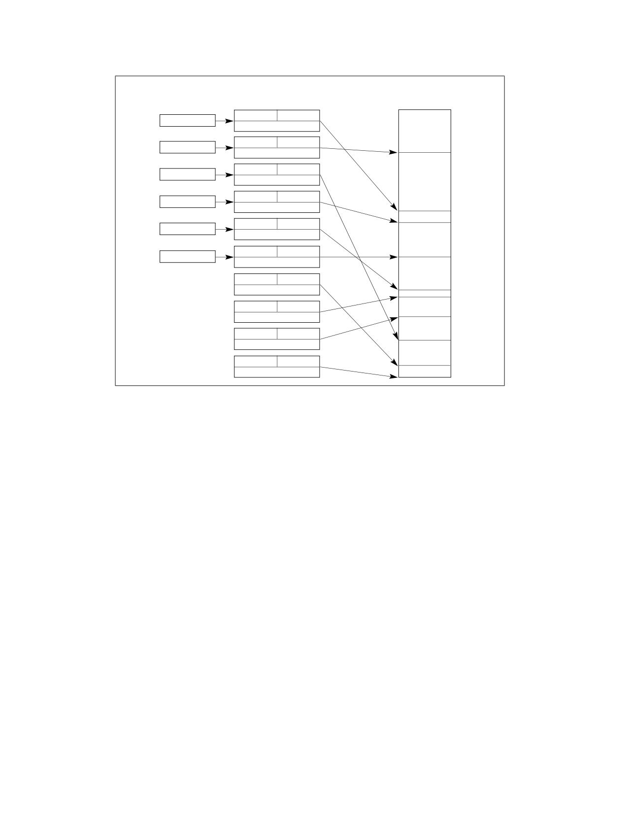
A multi-segment model (such as the one shown in Figure 3-4) uses the full capabilities of the segmentation mech-
anism to provide hardware enforced protection of code, data structures, and programs and tasks. Here, each
program (or task) is given its own table of segment descriptors and its own segments. The segments can be
completely private to their assigned programs or shared among programs. Access to all segments and to the
execution environments of individual programs running on the system is controlled by hardware.
3-4
Vol. 3A
PROTECTED-MODE MEMORY MANAGEMENT
Segment
Segment
Linear Address Space
Registers
Descriptors
(or Physical Memory)
Access
Limit
CS
Base Address
Stack
Access
Limit
SS
Base Address
Access
Limit
DS
Base Address
Code
Access
Limit
ES
Base Address
Data
Access
Limit
FS
Base Address
Data
Access
Limit
GS
Base Address
Data
Access
Limit
Base Address
Access
Limit
Base Address
Data
Access
Limit
Base Address
Access
Limit
Base Address
Figure 3-4. Multi-Segment Model
Access checks can be used to protect not only against referencing an address outside the limit of a segment, but
also against performing disallowed operations in certain segments. For example, since code segments are desig-
nated as read-only segments, hardware can be used to prevent writes into code segments. The access rights infor-
mation created for segments can also be used to set up protection rings or levels. Protection levels can be used to
protect operating-system procedures from unauthorized access by application programs.
3.2.4
Segmentation in IA-32e Mode
In IA-32e mode of Intel 64 architecture, the effects of segmentation depend on whether the processor is running
in compatibility mode or 64-bit mode. In compatibility mode, segmentation functions just as it does using legacy
16-bit or 32-bit protected mode semantics.
In 64-bit mode, segmentation is generally (but not completely) disabled, creating a flat 64-bit linear-address
space. The processor treats the segment base of CS, DS, ES, SS as zero, creating a linear address that is equal to
the effective address. The FS and GS segments are exceptions. These segment registers (which hold the segment
base) can be used as additional base registers in linear address calculations. They facilitate addressing local data
and certain operating system data structures.
Note that the processor does not perform segment limit checks at runtime in 64-bit mode.
3.2.5
Paging and Segmentation
Paging can be used with any of the segmentation models described in Figures 3-2, 3-3, and 3-4. The processor’s
paging mechanism divides the linear address space (into which segments are mapped) into pages (as shown in
Figure 3-1). These linear-address-space pages are then mapped to pages in the physical address space. The
paging mechanism offers several page-level protection facilities that can be used with or instead of the segment-
Vol. 3A
3-5
PROTECTED-MODE MEMORY MANAGEMENT
protection facilities. For example, it lets read-write protection be enforced on a page-by-page basis. The paging
mechanism also provides two-level user-supervisor protection that can also be specified on a page-by-page basis.
3.3
PHYSICAL ADDRESS SPACE
In protected mode, the IA-32 architecture provides a normal physical address space of 4 GBytes (232 bytes). This
is the address space that the processor can address on its address bus. This address space is flat (unsegmented),
with addresses ranging continuously from 0 to FFFFFFFFH. This physical address space can be mapped to read-
write memory, read-only memory, and memory mapped I/O. The memory mapping facilities described in this
chapter can be used to divide this physical memory up into segments and/or pages.
Starting with the Pentium Pro processor, the IA-32 architecture also supports an extension of the physical address
space to 236 bytes (64 GBytes); with a maximum physical address of FFFFFFFFFH. This extension is invoked in
either of two ways:
• Using the physical address extension (PAE) flag, located in bit 5 of control register CR4.
• Using the 36-bit page size extension (PSE-36) feature (introduced in the Pentium III processors).
Physical address support has since been extended beyond 36 bits. See Chapter 4, “Paging‚” for more information
about 36-bit physical addressing.
3.3.1
Intel® 64 Processors and Physical Address Space
On processors that support Intel 64 architecture (CPUID.80000001H:EDX[29] = 1), the size of the physical
address range is implementation-specific and indicated by CPUID.80000008H:EAX[bits 7-0].
For the format of information returned in EAX, see “CPUID-CPU Identification” in Chapter 3 of the Intel® 64 and
IA-32 Architectures Software Developer’s Manual, Volume 2A. See also: Chapter 4, “Paging.”
3.4
LOGICAL AND LINEAR ADDRESSES
At the system-architecture level in protected mode, the processor uses two stages of address translation to arrive
at a physical address: logical-address translation and linear address space paging.
Even with the minimum use of segments, every byte in the processor’s address space is accessed with a logical
address. A logical address consists of a 16-bit segment selector and a 32-bit offset (see Figure 3-5). The segment
selector identifies the segment the byte is located in and the offset specifies the location of the byte in the segment
relative to the base address of the segment.
The processor translates every logical address into a linear address. A linear address is a 32-bit address in the
processor’s linear address space. Like the physical address space, the linear address space is a flat (unsegmented),
232-byte address space, with addresses ranging from 0 to FFFFFFFFH. The linear address space contains all the
segments and system tables defined for a system.
To translate a logical address into a linear address, the processor does the following:
1. Uses the offset in the segment selector to locate the segment descriptor for the segment in the GDT or LDT and
reads it into the processor. (This step is needed only when a new segment selector is loaded into a segment
register.)
2. Examines the segment descriptor to check the access rights and range of the segment to ensure that the
segment is accessible and that the offset is within the limits of the segment.
3. Adds the base address of the segment from the segment descriptor to the offset to form a linear address.
3-6
Vol. 3A
PROTECTED-MODE MEMORY MANAGEMENT
15
0
31(63)
0
Logical
Seg. Selector
Offset (Effective Address)
Address
Descriptor Table
Base Address
Segment
+
Descriptor
31(63)
0
Linear Address
Figure 3-5. Logical Address to Linear Address Translation
If paging is not used, the processor maps the linear address directly to a physical address (that is, the linear
address goes out on the processor’s address bus). If the linear address space is paged, a second level of address
translation is used to translate the linear address into a physical address.
See also: Chapter 4, “Paging.”
3.4.1
Logical Address Translation in IA-32e Mode
In IA-32e mode, an Intel 64 processor uses the steps described above to translate a logical address to a linear
address. In 64-bit mode, the offset and base address of the segment are 64-bits instead of 32 bits. The linear
address format is also 64 bits wide and is subject to the canonical form requirement.
Each code segment descriptor provides an L bit. This bit allows a code segment to execute 64-bit code or legacy
32-bit code by code segment.
3.4.2
Segment Selectors
A segment selector is a 16-bit identifier for a segment (see Figure 3-6). It does not point directly to the segment,
but instead points to the segment descriptor that defines the segment. A segment selector contains the following
items:
Index
(Bits 3 through 15) - Selects one of 8192 descriptors in the GDT or LDT. The processor multiplies
the index value by 8 (the number of bytes in a segment descriptor) and adds the result to the base
address of the GDT or LDT (from the GDTR or LDTR register, respectively).
TI (table indicator) flag
(Bit 2) - Specifies the descriptor table to use: clearing this flag selects the GDT; setting this flag
selects the current LDT.
15
3
2
1
0
T
Index
RPL
I
Table Indicator
0 = GDT
1 = LDT
Requested Privilege Level (RPL)
Figure 3-6. Segment Selector
Vol. 3A
3-7
PROTECTED-MODE MEMORY MANAGEMENT
Requested Privilege Level (RPL)
(Bits 0 and 1) - Specifies the privilege level of the selector. The privilege level can range from 0 to
3, with 0 being the most privileged level. See Section 5.5, “Privilege Levels,” for a description of the
relationship of the RPL to the CPL of the executing program (or task) and the descriptor privilege
level (DPL) of the descriptor the segment selector points to.
The first entry of the GDT is not used by the processor. A segment selector that points to this entry of the GDT (that
is, a segment selector with an index of 0 and the TI flag set to 0) is used as a “null segment selector.” The processor
does not generate an exception when a segment register (other than the CS or SS registers) is loaded with a null
selector. It does, however, generate an exception when a segment register holding a null selector is used to access
memory. A null selector can be used to initialize unused segment registers. Loading the CS or SS register with a null
segment selector causes a general-protection exception (#GP) to be generated.
Segment selectors are visible to application programs as part of a pointer variable, but the values of selectors are
usually assigned or modified by link editors or linking loaders, not application programs.
3.4.3
Segment Registers
To reduce address translation time and coding complexity, the processor provides registers for holding up to 6
segment selectors (see Figure 3-7). Each of these segment registers support a specific kind of memory reference
(code, stack, or data). For virtually any kind of program execution to take place, at least the code-segment (CS),
data-segment (DS), and stack-segment (SS) registers must be loaded with valid segment selectors. The processor
also provides three additional data-segment registers (ES, FS, and GS), which can be used to make additional data
segments available to the currently executing program (or task).
For a program to access a segment, the segment selector for the segment must have been loaded in one of the
segment registers. So, although a system can define thousands of segments, only 6 can be available for immediate
use. Other segments can be made available by loading their segment selectors into these registers during program
execution.
Visible Part
Hidden Part
Segment Selector
Base Address, Limit, Access Information
CS
SS
DS
ES
FS
GS
Figure 3-7. Segment Registers
Every segment register has a “visible” part and a “hidden” part. (The hidden part is sometimes referred to as a
“descriptor cache” or a “shadow register.”) When a segment selector is loaded into the visible part of a segment
register, the processor also loads the hidden part of the segment register with the base address, segment limit, and
access control information from the segment descriptor pointed to by the segment selector. The information cached
in the segment register (visible and hidden) allows the processor to translate addresses without taking extra bus
cycles to read the base address and limit from the segment descriptor. In systems in which multiple processors
have access to the same descriptor tables, it is the responsibility of software to reload the segment registers when
the descriptor tables are modified. If this is not done, an old segment descriptor cached in a segment register might
be used after its memory-resident version has been modified.
Two kinds of load instructions are provided for loading the segment registers:
1. Direct load instructions such as the MOV, POP, LDS, LES, LSS, LGS, and LFS instructions. These instructions
explicitly reference the segment registers.
2. Implied load instructions such as the far pointer versions of the CALL, JMP, and RET instructions, the SYSENTER
and SYSEXIT instructions, and the IRET, INT n, INTO, INT3, and INT1 instructions. These instructions change
3-8
Vol. 3A
PROTECTED-MODE MEMORY MANAGEMENT
the contents of the CS register (and sometimes other segment registers) as an incidental part of their
operation.
The MOV instruction can also be used to store the visible part of a segment register in a general-purpose register.
3.4.4
Segment Loading Instructions in IA-32e Mode
Because ES, DS, and SS segment registers are not used in 64-bit mode, their fields (base, limit, and attribute) in
segment descriptor registers are ignored. Some forms of segment load instructions are also invalid (for example,
LDS, POP ES). Address calculations that reference the ES, DS, or SS segments are treated as if the segment base
is zero.
The processor checks that all linear-address references are in canonical form instead of performing limit checks.
Mode switching does not change the contents of the segment registers or the associated descriptor registers.
These registers are also not changed during 64-bit mode execution, unless explicit segment loads are performed.
In order to set up compatibility mode for an application, segment-load instructions (MOV to Sreg, POP Sreg) work
normally in 64-bit mode. An entry is read from the system descriptor table (GDT or LDT) and is loaded in the hidden
portion of the segment register. The descriptor-register base, limit, and attribute fields are all loaded. However, the
contents of the data and stack segment selector and the descriptor registers are ignored.
When FS and GS segment overrides are used in 64-bit mode, their respective base addresses are used in the linear
address calculation: (FS or GS).base + index + displacement. FS.base and GS.base are then expanded to the full
linear-address size supported by the implementation. The resulting effective address calculation can wrap across
positive and negative addresses; the resulting linear address must be canonical.
In 64-bit mode, memory accesses using FS-segment and GS-segment overrides are not checked for a runtime limit
nor subjected to attribute-checking. Normal segment loads (MOV to Sreg and POP Sreg) into FS and GS load a
standard 32-bit base value in the hidden portion of the segment register. The base address bits above the standard
32 bits are cleared to 0 to allow consistency for implementations that use less than 64 bits.
The hidden descriptor register fields for FS.base and GS.base are physically mapped to MSRs in order to load all
address bits supported by a 64-bit implementation. Software with CPL = 0 (privileged software) can load all
supported linear-address bits into FS.base or GS.base using WRMSR. Addresses written into the 64-bit FS.base
and GS.base registers must be in canonical form. A WRMSR instruction that attempts to write a non-canonical
address to those registers causes a #GP fault.
When in compatibility mode, FS and GS overrides operate as defined by 32-bit mode behavior regardless of the
value loaded into the upper 32 linear-address bits of the hidden descriptor register base field. Compatibility mode
ignores the upper 32 bits when calculating an effective address.
A new 64-bit mode instruction, SWAPGS, can be used to load GS base. SWAPGS exchanges the kernel data struc-
ture pointer from the IA32_KERNEL_GS_BASE MSR with the GS base register. The kernel can then use the GS
prefix on normal memory references to access the kernel data structures. An attempt to write a non-canonical
value (using WRMSR) to the IA32_KERNEL_GS_BASE MSR causes a #GP fault.
3.4.5
Segment Descriptors
A segment descriptor is a data structure in a GDT or LDT that provides the processor with the size and location of
a segment, as well as access control and status information. Segment descriptors are typically created by
compilers, linkers, loaders, or the operating system or executive, but not application programs. Figure 3-8 illus-
trates the general descriptor format for all types of segment descriptors.
Vol. 3A
3-9
PROTECTED-MODE MEMORY MANAGEMENT
31
2423 22 21 20 19
16 15 14 13 12 11
8
7
0
D
A
Seg.
D
Base 31:24
G
/
L
V
Limit
P
P
S
Type
Base 23:16
4
B
L
19:16
L
31
16 15
0
Base Address 15:00
Segment Limit 15:00
0
L
- 64-bit code segment (IA-32e mode only)
AVL
- Available for use by system software
BASE - Segment base address
D/B
- Default operation size (0 = 16-bit segment; 1 = 32-bit segment)
DPL
- Descriptor privilege level
G
- Granularity
LIMIT - Segment Limit
P
- Segment present
S
- Descriptor type (0 = system; 1 = code or data)
TYPE - Segment type
Figure 3-8. Segment Descriptor
The flags and fields in a segment descriptor are as follows:
Segment limit field
Specifies the size of the segment. The processor puts together the two segment limit fields to form
a 20-bit value. The processor interprets the segment limit in one of two ways, depending on the
setting of the G (granularity) flag:
• If the granularity flag is clear, the segment size can range from 1 byte to 1 MByte, in byte incre-
ments.
• If the granularity flag is set, the segment size can range from 4 KBytes to 4 GBytes, in 4-KByte
increments.
The processor uses the segment limit in two different ways, depending on whether the segment is
an expand-up or an expand-down segment. See Section 3.4.5.1, “Code- and Data-Segment
Descriptor Types,” for more information about segment types. For expand-up segments, the offset
in a logical address can range from 0 to the segment limit. Offsets greater than the segment limit
generate general-protection exceptions (#GP, for all segments other than SS) or stack-fault excep-
tions (#SS for the SS segment). For expand-down segments, the segment limit has the reverse
function; the offset can range from the segment limit plus 1 to FFFFFFFFH or FFFFH, depending on
the setting of the B flag. Offsets less than or equal to the segment limit generate general-protection
exceptions or stack-fault exceptions. Decreasing the value in the segment limit field for an expand-
down segment allocates new memory at the bottom of the segment's address space, rather than at
the top. IA-32 architecture stacks always grow downwards, making this mechanism convenient for
expandable stacks.
Base address fields
Defines the location of byte 0 of the segment within the 4-GByte linear address space. The
processor puts together the three base address fields to form a single 32-bit value. Segment base
addresses should be aligned to 16-byte boundaries. Although 16-byte alignment is not required,
this alignment allows programs to maximize performance by aligning code and data on 16-byte
boundaries.
Type field
Indicates the segment or gate type and specifies the kinds of access that can be made to the
segment and the direction of growth. The interpretation of this field depends on whether the
descriptor type flag specifies an application (code or data) descriptor or a system descriptor. The
encoding of the type field is different for code, data, and system descriptors (see Figure 5-1). See
Section 3.4.5.1, “Code- and Data-Segment Descriptor Types,” for a description of how this field is
used to specify code and data-segment types.
3-10
Vol. 3A
PROTECTED-MODE MEMORY MANAGEMENT
S (descriptor type) flag
Specifies whether the segment descriptor is for a system segment (S flag is clear) or a code or data
segment (S flag is set).
DPL (descriptor privilege level) field
Specifies the privilege level of the segment. The privilege level can range from 0 to 3, with 0 being
the most privileged level. The DPL is used to control access to the segment. See Section 5.5, “Priv-
ilege Levels,” for a description of the relationship of the DPL to the CPL of the executing code
segment and the RPL of a segment selector.
P (segment-present) flag
Indicates whether the segment is present in memory (set) or not present (clear). If this flag is clear,
the processor generates a segment-not-present exception (#NP) when a segment selector that
points to the segment descriptor is loaded into a segment register. Memory management software
can use this flag to control which segments are actually loaded into physical memory at a given
time. It offers a control in addition to paging for managing virtual memory.
Figure 3-9 shows the format of a segment descriptor when the segment-present flag is clear. When
this flag is clear, the operating system or executive is free to use the locations marked “Available” to
store its own data, such as information regarding the whereabouts of the missing segment.
D/B (default operation size/default stack pointer size and/or upper bound) flag
Performs different functions depending on whether the segment descriptor is an executable code
segment, an expand-down data segment, or a stack segment. (This flag should always be set to 1
for 32-bit code and data segments and to 0 for 16-bit code and data segments.)
• Executable code segment. The flag is called the D flag and it indicates the default length for
effective addresses and operands referenced by instructions in the segment. If the flag is set,
32-bit addresses and 32-bit or 8-bit operands are assumed; if it is clear, 16-bit addresses and
16-bit or 8-bit operands are assumed.
The instruction prefix 66H can be used to select an operand size other than the default, and the
prefix 67H can be used select an address size other than the default.
• Stack segment (data segment pointed to by the SS register). The flag is called the B (big)
flag and it specifies the size of the stack pointer used for implicit stack operations (such as
pushes, pops, and calls). If the flag is set, a 32-bit stack pointer is used, which is stored in the
32-bit ESP register; if the flag is clear, a 16-bit stack pointer is used, which is stored in the 16-
bit SP register. If the stack segment is set up to be an expand-down data segment (described in
the next paragraph), the B flag also specifies the upper bound of the stack segment.
• Expand-down data segment. The flag is called the B flag and it specifies the upper bound of
the segment. If the flag is set, the upper bound is FFFFFFFFH (4 GBytes); if the flag is clear, the
upper bound is FFFFH (64 KBytes).
31
16 15 14 13 12 11
8 7
0
D
Available
0
P
S
Type
Available
4
L
31
0
Available
0
Figure 3-9. Segment Descriptor When Segment-Present Flag Is Clear
G (granularity) flag
Determines the scaling of the segment limit field. When the granularity flag is clear, the segment
limit is interpreted in byte units; when flag is set, the segment limit is interpreted in 4-KByte units.
(This flag does not affect the granularity of the base address; it is always byte granular.) When the
granularity flag is set, the twelve least significant bits of an offset are not tested when checking the
Vol. 3A
3-11
PROTECTED-MODE MEMORY MANAGEMENT
offset against the segment limit. For example, when the granularity flag is set, a limit of 0 results in
valid offsets from 0 to 4095.
L (64-bit code segment) flag
In IA-32e mode, bit 21 of the second doubleword of the segment descriptor indicates whether a
code segment contains native 64-bit code. A value of 1 indicates instructions in this code segment
are executed in 64-bit mode. A value of 0 indicates the instructions in this code segment are
executed in compatibility mode. If the L-bit is set, then the D-bit must be cleared. Bit 21 is not used
outside IA-32e mode (or for data segments). Because an attempt to activate IA-32e mode will fault
if the current CS has the L-bit set (see Section 10.8.5), software operating outside IA-32e mode
should avoid loading CS from a descriptor that sets the L-bit.
Available and reserved bits
Bit 20 of the second doubleword of the segment descriptor is available for use by system software.
3.4.5.1
Code- and Data-Segment Descriptor Types
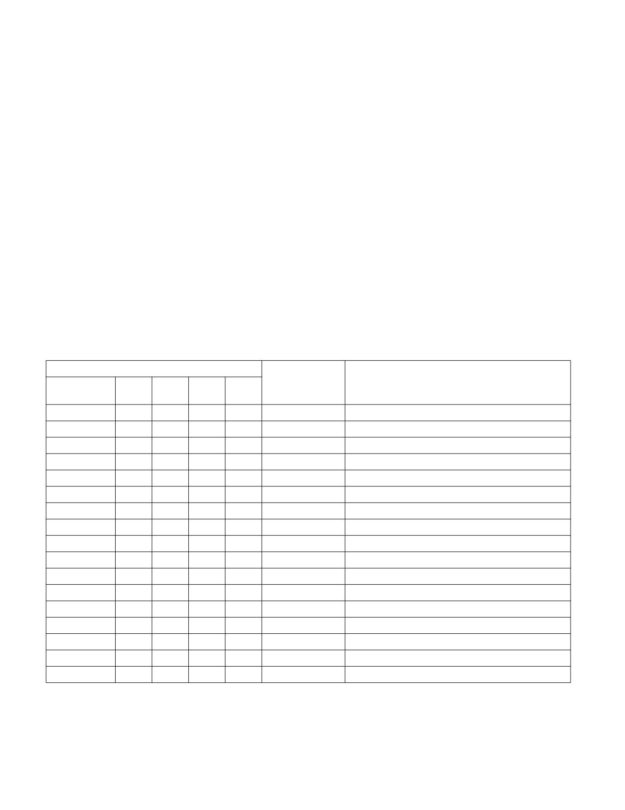
When the S (descriptor type) flag in a segment descriptor is set, the descriptor is for either a code or a data
segment. The highest order bit of the type field (bit 11 of the second double word of the segment descriptor) then
determines whether the descriptor is for a data segment (clear) or a code segment (set).
For data segments, the three low-order bits of the type field (bits 8, 9, and 10) are interpreted as accessed (A),
write-enable (W), and expansion-direction (E). See Table 3-1 for a description of the encoding of the bits in the
type field for code and data segments. Data segments can be read-only or read/write segments, depending on the
setting of the write-enable bit.
Table 3-1. Code- and Data-Segment Types
Type Field
Descriptor
Description
Type
Decimal
11
10
9
8
E
W
A
0
0
0
0
0
Data
Read-Only
1
0
0
0
1
Data
Read-Only, accessed
2
0
0
1
0
Data
Read/Write
3
0
0
1
1
Data
Read/Write, accessed
4
0
1
0
0
Data
Read-Only, expand-down
5
0
1
0
1
Data
Read-Only, expand-down, accessed
6
0
1
1
0
Data
Read/Write, expand-down
7
0
1
1
1
Data
Read/Write, expand-down, accessed
C
R
A
8
1
0
0
0
Code
Execute-Only
9
1
0
0
1
Code
Execute-Only, accessed
10
1
0
1
0
Code
Execute/Read
11
1
0
1
1
Code
Execute/Read, accessed
12
1
1
0
0
Code
Execute-Only, conforming
13
1
1
0
1
Code
Execute-Only, conforming, accessed
14
1
1
1
0
Code
Execute/Read, conforming
15
1
1
1
1
Code
Execute/Read, conforming, accessed
Stack segments are data segments which must be read/write segments. Loading the SS register with a segment
selector for a nonwritable data segment generates a general-protection exception (#GP). If the size of a stack
segment needs to be changed dynamically, the stack segment can be an expand-down data segment (expansion-
3-12
Vol. 3A
PROTECTED-MODE MEMORY MANAGEMENT
direction flag set). Here, dynamically changing the segment limit causes stack space to be added to the bottom of
the stack. If the size of a stack segment is intended to remain static, the stack segment may be either an expand-
up or expand-down type.
The accessed bit indicates whether the segment has been accessed since the last time the operating-system or
executive cleared the bit. The processor sets this bit whenever it loads a segment selector for the segment into a
segment register, assuming that the type of memory that contains the segment descriptor supports processor
writes. The bit remains set until explicitly cleared. This bit can be used both for virtual memory management and
for debugging.
For code segments, the three low-order bits of the type field are interpreted as accessed (A), read enable (R), and
conforming (C). Code segments can be execute-only or execute/read, depending on the setting of the read-enable
bit. An execute/read segment might be used when constants or other static data have been placed with instruction
code in a ROM. Here, data can be read from the code segment either by using an instruction with a CS override
prefix or by loading a segment selector for the code segment in a data-segment register (the DS, ES, FS, or GS
registers). In protected mode, code segments are not writable.
Code segments can be either conforming or nonconforming. A transfer of execution into a more-privileged
conforming segment allows execution to continue at the current privilege level. A transfer into a nonconforming
segment at a different privilege level results in a general-protection exception (#GP), unless a call gate or task gate
is used (see Section 5.8.1, “Direct Calls or Jumps to Code Segments,” for more information on conforming and
nonconforming code segments). System utilities that do not access protected facilities and handlers for some types
of exceptions (such as, divide error or overflow) may be loaded in conforming code segments. Utilities that need to
be protected from less privileged programs and procedures should be placed in nonconforming code segments.
NOTE
Execution cannot be transferred by a call or a jump to a less-privileged (numerically higher
privilege level) code segment, regardless of whether the target segment is a conforming or
nonconforming code segment. Attempting such an execution transfer will result in a general-
protection exception.
All data segments are nonconforming, meaning that they cannot be accessed by less privileged programs or proce-
dures (code executing at numerically higher privilege levels). Unlike code segments, however, data segments can
be accessed by more privileged programs or procedures (code executing at numerically lower privilege levels)
without using a special access gate.
If the segment descriptors in the GDT or an LDT are placed in ROM, the processor can enter an indefinite loop if
software or the processor attempts to update (write to) the ROM-based segment descriptors. To prevent this
problem, set the accessed bits for all segment descriptors placed in a ROM. Also, remove operating-system or
executive code that attempts to modify segment descriptors located in ROM.
3.5
SYSTEM DESCRIPTOR TYPES
When the S (descriptor type) flag in a segment descriptor is clear, the descriptor type is a system descriptor. The
processor recognizes the following types of system descriptors:
• Local descriptor-table (LDT) segment descriptor.
• Task-state segment (TSS) descriptor.
• Call-gate descriptor.
• Interrupt-gate descriptor.
• Trap-gate descriptor.
• Task-gate descriptor.
These descriptor types fall into two categories: system-segment descriptors and gate descriptors. System-
segment descriptors point to system segments (LDT and TSS segments). Gate descriptors are in themselves
“gates,” which hold pointers to procedure entry points in code segments (call, interrupt, and trap gates) or which
hold segment selectors for TSS’s (task gates).
Vol. 3A
3-13
PROTECTED-MODE MEMORY MANAGEMENT
Table 3-2 shows the encoding of the type field for system-segment descriptors and gate descriptors. Note that
system descriptors in IA-32e mode are 16 bytes instead of 8 bytes.
Table 3-2. System-Segment and Gate-Descriptor Types
Type Field
Description
Decimal
11
10
9
8
32-Bit Mode
IA-32e Mode
0
0
0
0
0
Reserved
Reserved
1
0
0
0
1
16-bit TSS (Available)
Reserved
2
0
0
1
0
LDT
LDT
3
0
0
1
1
16-bit TSS (Busy)
Reserved
4
0
1
0
0
16-bit Call Gate
Reserved
5
0
1
0
1
Task Gate
Reserved
6
0
1
1
0
16-bit Interrupt Gate
Reserved
7
0
1
1
1
16-bit Trap Gate
Reserved
8
1
0
0
0
Reserved
Reserved
9
1
0
0
1
32-bit TSS (Available)
64-bit TSS (Available)
10
1
0
1
0
Reserved
Reserved
11
1
0
1
1
32-bit TSS (Busy)
64-bit TSS (Busy)
12
1
1
0
0
32-bit Call Gate
64-bit Call Gate
13
1
1
0
1
Reserved
Reserved
14
1
1
1
0
32-bit Interrupt Gate
64-bit Interrupt Gate
15
1
1
1
1
32-bit Trap Gate
64-bit Trap Gate
See also: Section 3.5.1, “Segment Descriptor Tables,” and Section 8.2.2, “TSS Descriptor,” (for more information
on the system-segment descriptors); see Section 5.8.3, “Call Gates,” Section 6.11, “IDT Descriptors,” and Section
8.2.5, “Task-Gate Descriptor,” (for more information on the gate descriptors).
3.5.1
Segment Descriptor Tables
A segment descriptor table is an array of segment descriptors (see Figure 3-10). A descriptor table is variable in
length and can contain up to 8192 (213) 8-byte descriptors. There are two kinds of descriptor tables:
• The global descriptor table (GDT).
• The local descriptor tables (LDT).
3-14
Vol. 3A
PROTECTED-MODE MEMORY MANAGEMENT
Global
Local
Descriptor
Descriptor
Table (GDT)
Table (LDT)
T
I
TI = 0
TI = 1
Segment
Selector
56
56
48
48
40
40
32
32
24
24
16
16
8
8
First Descriptor in
GDT is Not Used
0
0
GDTR Register
LDTR Register
Limit
Limit
Base Address
Base Address
Seg. Sel.
Figure 3-10. Global and Local Descriptor Tables
Each system must have one GDT defined, which may be used for all programs and tasks in the system. Optionally,
one or more LDTs can be defined. For example, an LDT can be defined for each separate task being run, or some or
all tasks can share the same LDT.
The GDT is not a segment itself; instead, it is a data structure in linear address space. The base linear address and
limit of the GDT must be loaded into the GDTR register (see Section 2.4, “Memory-Management Registers”). The
base address of the GDT should be aligned on an eight-byte boundary to yield the best processor performance. The
limit value for the GDT is expressed in bytes. As with segments, the limit value is added to the base address to get
the address of the last valid byte. A limit value of 0 results in exactly one valid byte. Because segment descriptors
are always 8 bytes long, the GDT limit should always be one less than an integral multiple of eight (that is, 8N - 1).
The first descriptor in the GDT is not used by the processor. A segment selector to this “null descriptor” does not
generate an exception when loaded into a data-segment register (DS, ES, FS, or GS), but it always generates a
general-protection exception (#GP) when an attempt is made to access memory using the descriptor. By initializing
the segment registers with this segment selector, accidental reference to unused segment registers can be guar-
anteed to generate an exception.
The LDT is located in a system segment of the LDT type. The GDT must contain a segment descriptor for the LDT
segment. If the system supports multiple LDTs, each must have a separate segment selector and segment
descriptor in the GDT. The segment descriptor for an LDT can be located anywhere in the GDT. See Section 3.5,
“System Descriptor Types,” for information on the LDT segment-descriptor type.
An LDT is accessed with its segment selector. To eliminate address translations when accessing the LDT, the
segment selector, base linear address, limit, and access rights of the LDT are stored in the LDTR register (see
Section 2.4, “Memory-Management Registers”).
When the GDTR register is stored (using the SGDT instruction), a 48-bit “pseudo-descriptor” is stored in memory
(see top diagram in Figure 3-11). To avoid alignment check faults in user mode (privilege level 3), the pseudo-
descriptor should be located at an odd word address (that is, address MOD 4 is equal to 2). This causes the
Vol. 3A
3-15
PROTECTED-MODE MEMORY MANAGEMENT
processor to store an aligned word, followed by an aligned doubleword. User-mode programs normally do not store
pseudo-descriptors, but the possibility of generating an alignment check fault can be avoided by aligning pseudo-
descriptors in this way. The same alignment should be used when storing the IDTR register using the SIDT instruc-
tion. When storing the LDTR or task register (using the SLDT or STR instruction, respectively), the pseudo-
descriptor should be located at a doubleword address (that is, address MOD 4 is equal to 0).
47
16 15
0
32-bit Base Address
Limit
79
16 15
0
64-bit Base Address
Limit
Figure 3-11. Pseudo-Descriptor Formats
3.5.2
Segment Descriptor Tables in IA-32e Mode
In IA-32e mode, a segment descriptor table can contain up to 8192 (213) 8-byte descriptors. An entry in the
segment descriptor table can be 8 bytes. System descriptors are expanded to 16 bytes (occupying the space of two
entries).
GDTR and LDTR registers are expanded to hold 64-bit base address. The corresponding pseudo-descriptor is 80
bits. (see the bottom diagram in Figure 3-11).
The following system descriptors expand to 16 bytes:
- Call gate descriptors (see Section 5.8.3.1, “IA-32e Mode Call Gates”).
- IDT gate descriptors (see Section 6.14.1, “64-Bit Mode IDT”).
- LDT and TSS descriptors (see Section 8.2.3, “TSS Descriptor in 64-bit mode”).
3-16
Vol. 3A
CHAPTER 4
PAGING
Chapter 3 explains how segmentation converts logical addresses to linear addresses. Paging (or linear-address
translation) is the process of translating linear addresses so that they can be used to access memory or I/O
devices. Paging translates each linear address to a physical address and determines, for each translation, what
accesses to the linear address are allowed (the address’s access rights) and the type of caching used for such
accesses (the address’s memory type).
Intel-64 processors support four different paging modes. These modes are identified and defined in Section 4.1.
Section 4.2 gives an overview of the translation mechanism that is used in all modes. Section 4.3, Section 4.4, and
Section 4.5 discuss the four paging modes in detail.
Section 4.6 details how paging determines and uses access rights. Section 4.7 discusses exceptions that may be
generated by paging (page-fault exceptions). Section 4.8 considers data which the processor writes in response to
linear-address accesses (accessed and dirty flags).
Section 4.9 describes how paging determines the memory types used for accesses to linear addresses. Section
4.10 provides details of how a processor may cache information about linear-address translation. Section 4.11
outlines interactions between paging and certain VMX features. Section 4.12 gives an overview of how paging can
be used to implement virtual memory.
4.1
PAGING MODES AND CONTROL BITS
Paging behavior is controlled by the following control bits:
• The WP and PG flags in control register CR0 (bit 16 and bit 31, respectively).
• The PSE, PAE, PGE, LA57, PCIDE, SMEP, SMAP, PKE, CET, and PKS flags in control register CR4 (bit 4, bit 5,
bit 7, bit 12, bit 17, bit 20, bit 21, bit 22, bit 23, and bit 24, respectively).
• The LME and NXE flags in the IA32_EFER MSR (bit 8 and bit 11, respectively).
• The AC flag in the EFLAGS register (bit 18).
• The “enable HLAT” VM-execution control (tertiary processor-based VM-execution control bit 1; see Section
25.6.2, “Processor-Based VM-Execution Controls,” in the Intel® 64 and IA-32 Architectures Software
Developer’s Manual, Volume 3C).
Software enables paging by using the MOV to CR0 instruction to set CR0.PG. Before doing so, software should
ensure that control register CR3 contains the physical address of the first paging structure that the processor will
use for linear-address translation (see Section 4.2) and that that structure is initialized as desired. See Table 4-3,
Table 4-7, and Table 4-12 for the use of CR3 in the different paging modes.
Section 4.1.1 describes how the values of CR0.PG, CR4.PAE, CR4.LA57, and IA32_EFER.LME determine whether
paging is enabled and, if so, which of four paging modes is in use. Section 4.1.2 explains how to manage these bits
to establish or make changes in paging modes. Section 4.1.3 discusses how CR0.WP, CR4.PSE, CR4.PGE,
CR4.PCIDE, CR4.SMEP, CR4.SMAP, CR4.PKE, CR4.CET, CR4.PKS, and IA32_EFER.NXE modify the operation of the
different paging modes.
4.1.1
Four Paging Modes
If CR0.PG = 0, paging is not used. The logical processor treats all linear addresses as if they were physical
addresses. CR4.PAE, CR4.LA57, and IA32_EFER.LME are ignored by the processor, as are CR0.WP, CR4.PSE,
CR4.PGE, CR4.SMEP, CR4.SMAP, and IA32_EFER.NXE. (CR4.CET is also ignored insofar as it affects linear-address
access rights.)
Paging is enabled if CR0.PG = 1. Paging can be enabled only if protection is enabled (CR0.PE = 1). If paging is
enabled, one of four paging modes is used. The values of CR4.PAE, CR4.LA57, and IA32_EFER.LME determine
which paging mode is used:
Vol. 3A
4-1
PAGING
• If CR4.PAE = 0, 32-bit paging is used. 32-bit paging is detailed in Section 4.3. 32-bit paging uses CR0.WP,
CR4.PSE, CR4.PGE, CR4.SMEP, CR4.SMAP, and CR4.CET as described in Section 4.1.3 and Section 4.6.
• If CR4.PAE = 1 and IA32_EFER.LME = 0, PAE paging is used. PAE paging is detailed in Section 4.4. PAE paging
uses CR0.WP, CR4.PGE, CR4.SMEP, CR4.SMAP, CR4.CET, and IA32_EFER.NXE as described in Section 4.1.3 and
Section 4.6.
• If CR4.PAE = 1, IA32_EFER.LME = 1, and CR4.LA57 = 0, 4-level paging1 is used.2 4-level paging is detailed
in Section 4.5 (along with 5-level paging). 4-level paging uses CR0.WP, CR4.PGE, CR4.PCIDE, CR4.SMEP,
CR4.SMAP, CR4.PKE, CR4.CET, CR4.PKS, and IA32_EFER.NXE as described in Section 4.1.3 and Section 4.6.
• If CR4.PAE = 1, IA32_EFER.LME = 1, and CR4.LA57 = 1, 5-level paging is used. 5-level paging is detailed in
Section 4.5 (along with 4-level paging). 5-level paging uses CR0.WP, CR4.PGE, CR4.PCIDE, CR4.SMEP,
CR4.SMAP, CR4.PKE, CR4.CET, CR4.PKS, and IA32_EFER.NXE as described in Section 4.1.3 and Section 4.6.
NOTE
32-bit paging and PAE paging can be used only in legacy protected mode (IA32_EFER.LME = 0). In
contrast, 4-level paging and 5-level paging can be used only IA-32e mode (IA32_EFER.LME = 1).
The four paging modes differ with regard to the following details:
• Linear-address width. The size of the linear addresses that can be translated.
• Physical-address width. The size of the physical addresses produced by paging.
• Page size. The granularity at which linear addresses are translated. Linear addresses on the same page are
translated to corresponding physical addresses on the same page.
• Support for execute-disable access rights. In some paging modes, software can be prevented from fetching
instructions from pages that are otherwise readable.
• Support for PCIDs. With 4-level paging and 5-level paging, software can enable a facility by which a logical
processor caches information for multiple linear-address spaces. The processor may retain cached information
when software switches between different linear-address spaces.
• Support for protection keys. With 4-level paging and 5-level paging, each linear address is associated with a
protection key. Software can use the protection-key rights registers to disable, for each protection key, how
certain accesses to linear addresses associated with that protection key.
Table 4-1 illustrates the principal differences between the four paging modes.
Table 4-1. Properties of Different Paging Modes
Supports
Lin.-
Phys.-
Supports
Paging
PG in
PAE in
LME in
LA57 in
Page
PCIDs and
Addr.
Addr.
Execute-
Mode
CR0
CR4
IA32_EFER
CR4
Sizes
protection
Width
Width1
Disable?
keys?
None
0
N/A
N/A
N/A
32
32
N/A
No
No
4 KB
32-bit
1
0
02
N/A
32
Up to 403
No
No
4 MB4
4 KB
PAE
1
1
0
N/A
32
Up to 52
Yes5
No
2 MB
4 KB
4-level
1
1
1
0
48
Up to 52
2 MB
Yes5
Yes7
1 GB6
1. Earlier versions of this manual used the term “IA-32e paging” to identify 4-level paging.
2. The LMA flag in the IA32_EFER MSR (bit 10) is a status bit that indicates whether the logical processor is in IA-32e mode (and thus
uses either 4-level paging or 5-level paging). The processor always sets IA32_EFER.LMA to CR0.PG & IA32_EFER.LME. Software can-
not directly modify IA32_EFER.LMA; an execution of WRMSR to the IA32_EFER MSR ignores bit 10 of its source operand.
4-2
Vol. 3A
PAGING
Table 4-1. Properties of Different Paging Modes (Contd.)
Supports
Lin.-
Phys.-
Supports
Paging
PG in
PAE in
LME in
LA57 in
Page
PCIDs and
Addr.
Addr.
Execute-
Mode
CR0
CR4
IA32_EFER
CR4
Sizes
protection
Width
Width1
Disable?
keys?
4 KB
5-level
1
1
1
1
57
Up to 52
2 MB
Yes5
Yes7
1 GB6
NOTES:
1. The physical-address width is always bounded by MAXPHYADDR; see Section 4.1.4.
2. The processor ensures that IA32_EFER.LME must be 0 if CR0.PG = 1 and CR4.PAE = 0.
3. 32-bit paging supports physical-address widths of more than 32 bits only for 4-MByte pages and only if the PSE-36 mechanism is
supported; see Section 4.1.4 and Section 4.3.
4. 32-bit paging uses 4-MByte pages only if CR4.PSE = 1; see Section 4.3.
5. Execute-disable access rights are applied only if IA32_EFER.NXE = 1; see Section 4.6.
6. Processors that support 4-level paging or 5-level paging do not necessarily support 1-GByte pages; see Section 4.1.4.
7. PCIDs are used only if CR4.PCIDE = 1; see Section 4.10.1. Protection keys are used only if certain conditions hold; see Section 4.6.2.
Because 32-bit paging and PAE paging are used only in legacy protected mode and because legacy protected mode
cannot produce linear addresses larger than 32 bits, 32-bit paging and PAE paging translate 32-bit linear
addresses.
4-level paging and 5-level paging are used only in IA-32e mode. IA-32e mode has two sub-modes:
• Compatibility mode. This sub-mode uses only 32-bit linear addresses. In this sub-mode, 4-level paging and 5-
level paging treat bits 63:32 of such an address as all 0.
•
64-bit mode. While this sub-mode produces 64-bit linear addresses, the processor enforces canonicality,
meaning that the upper bits of such an address are identical: bits 63:47 for 4-level paging and bits 63:56 for
5-level paging. 4-level paging (respectively, 5-level paging) does not use bits 63:48 (respectively, bits 63:57)
of such addresses.
4.1.2
Paging-Mode Enabling
If CR0.PG = 1, a logical processor is in one of four paging modes, depending on the values of CR4.PAE,
IA32_EFER.LME, and CR4.LA57. Figure 4-1 illustrates how software can enable these modes and make transitions
between them. The following items identify certain limitations and other details:
• IA32_EFER.LME cannot be modified while paging is enabled (CR0.PG = 1). Attempts to do so using WRMSR
cause a general-protection exception (#GP(0)).
• Paging cannot be enabled (by setting CR0.PG to 1) while CR4.PAE = 0 and IA32_EFER.LME = 1. Attempts to do
so using MOV to CR0 cause a general-protection exception (#GP(0)).
• One node in Figure 4-1 is labeled “IA-32e mode.” This node represents either 4-level paging (if CR4.LA57 = 0)
or 5-level paging (if CR4.LA57 = 1). As noted in the following items, software cannot modify CR4.LA57
(effecting transition between 4-level paging and 5-level paging) without first disabling paging.
• CR4.PAE and CR4.LA57 cannot be modified while either 4-level paging or 5-level paging is in use (when
CR0.PG = 1 and IA32_EFER.LME = 1). Attempts to do so using MOV to CR4 cause a general-protection
exception (#GP(0)).
• Regardless of the current paging mode, software can disable paging by clearing CR0.PG with MOV to CR0.1
• Software can transition between 32-bit paging and PAE paging by changing the value of CR4.PAE with MOV to
CR4.
1. If the logical processor is in 64-bit mode or if CR4.PCIDE = 1, an attempt to clear CR0.PG causes a general-protection exception
(#GP). Software should transition to compatibility mode and clear CR4.PCIDE before attempting to disable paging.
Vol. 3A
4-3
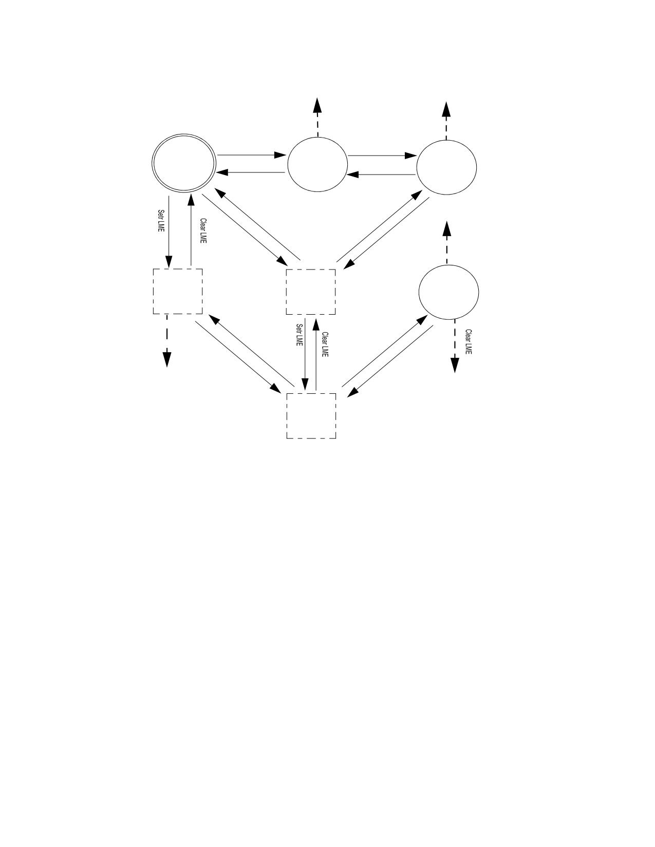
PAGING
#GP
#GP
Set LME
Set LME
No Paging
Set PG
32-bit Paging
Set PAE
PAE Paging
PG = 0
PG = 1
PG = 1
PAE = 0
PAE = 0
PAE = 1
LME = 0
Clear PG
LME = 0
Clear PAE
LME = 0
#GP
Clear PAE
Set PG
Clear PAE
Set PAE
Clear PG
No Paging
No Paging
4-level Paging
PG = 0
PG = 0
PG = 1
PAE = 0
PAE = 1
PAE = 1
LME = 1
LME = 0
LME = 1
Set PG
Set PG
Clear PAE
Clear PG
Set PAE
#GP
#GP
No Paging
PG = 0
PAE = 1
LME = 1
Figure 4-1. Enabling and Changing Paging Modes
•
Software cannot transition directly between 4-level paging (or 5-level paging) and any of other paging mode.
It must first disable paging (by clearing CR0.PG with MOV to CR0), then set CR4.PAE, IA32_EFER.LME, and
CR4.LA57 to the desired values (with MOV to CR4 and WRMSR), and then re-enable paging (by setting CR0.PG
with MOV to CR0). As noted earlier, an attempt to modify CR4.PAE, IA32_EFER.LME, or CR.LA57 while 4-level
paging or 5-level paging is enabled causes a general-protection exception (#GP(0)).
•
VMX transitions allow transitions between paging modes that are not possible using MOV to CR or WRMSR. This
is because VMX transitions can load CR0, CR4, and IA32_EFER in one operation. See Section 4.11.1.
4.1.3
Paging-Mode Modifiers
Details of how each paging mode operates are determined by the following control bits:
• The WP flag in CR0 (bit 16).
• The PSE, PGE, PCIDE, SMEP, SMAP, PKE, CET, and PKS flags in CR4 (bit 4, bit 7, bit 17, bit 20, bit 21, bit 22,
bit 23, and bit 24, respectively).
• The NXE flag in the IA32_EFER MSR (bit 11).
• The “enable HLAT” VM-execution control (tertiary processor-based VM-execution control bit 1).
CR0.WP allows pages to be protected from supervisor-mode writes. If CR0.WP = 0, supervisor-mode write
accesses are allowed to linear addresses with read-only access rights; if CR0.WP = 1, they are not. (User-mode
write accesses are never allowed to linear addresses with read-only access rights, regardless of the value of
4-4
Vol. 3A
PAGING
CR0.WP.) Section 4.6 explains how access rights are determined, including the definition of supervisor-mode and
user-mode accesses.
CR4.PSE enables 4-MByte pages for 32-bit paging. If CR4.PSE = 0, 32-bit paging can use only 4-KByte pages; if
CR4.PSE = 1, 32-bit paging can use both 4-KByte pages and 4-MByte pages. See Section 4.3 for more information.
(PAE paging, 4-level paging, and 5-level paging can use multiple page sizes regardless of the value of CR4.PSE.)
CR4.PGE enables global pages. If CR4.PGE = 0, no translations are shared across address spaces; if CR4.PGE = 1,
specified translations may be shared across address spaces. See Section 4.10.2.4 for more information.
CR4.PCIDE enables process-context identifiers (PCIDs) for 4-level paging and 5-level paging. PCIDs allow a logical
processor to cache information for multiple linear-address spaces. See Section 4.10.1 for more information.
CR4.SMEP allows pages to be protected from supervisor-mode instruction fetches. If CR4.SMEP = 1, software
operating in supervisor mode cannot fetch instructions from linear addresses that are accessible in user mode.
Section 4.6 explains how access rights are determined, including the definition of supervisor-mode accesses and
user-mode accessibility.
CR4.SMAP allows pages to be protected from supervisor-mode data accesses. If CR4.SMAP = 1, software oper-
ating in supervisor mode cannot access data at linear addresses that are accessible in user mode. Software can
override this protection by setting EFLAGS.AC. Section 4.6 explains how access rights are determined, including
the definition of supervisor-mode accesses and user-mode accessibility.
CR4.PKE and CR4.PKS enable specification of access rights based on protection keys. 4-level paging and 5-level
paging associate each linear address with a protection key. When CR4.PKE = 1, the PKRU register specifies, for
each protection key, whether user-mode linear addresses with that protection key can be read or written. When
CR4.PKS = 1, the IA32_PKRS MSR does the same for supervisor-mode linear addresses. See Section 4.6 for more
information.
CR4.CET enables control-flow enforcement technology, including the shadow-stack feature. If CR4.CET = 1,
certain memory accesses are identified as shadow-stack accesses and certain linear addresses translate to
shadow-stack pages. Section 4.6 explains how access rights are determined for these accesses and pages. (The
processor allows CR4.CET to be set only if CR0.WP is also set.)
IA32_EFER.NXE enables execute-disable access rights for PAE paging, 4-level paging, and 5-level paging. If
IA32_EFER.NXE = 1, instruction fetches can be prevented from specified linear addresses (even if data reads from
the addresses are allowed). Section 4.6 explains how access rights are determined. (IA32_EFER.NXE has no effect
with 32-bit paging. Software that wants to use this feature to limit instruction fetches from readable pages must
use PAE paging, 4-level paging, or 5-level paging.)
The “enable HLAT” VM-execution control enables HLAT paging for 4-level paging and 5-level paging. HLAT paging
does not use control register CR3 to identify the address of the first paging structure used for linear-address trans-
lation; instead, that structure is located using a field in the virtual-machine control structure (VMCS). In addition,
HLAT paging interprets certain bits in paging-structure entries differently than ordinary paging. See Section 4.5 for
details.
4.1.4
Enumeration of Paging Features by CPUID
Software can discover support for different paging features using the CPUID instruction:
• PSE: page-size extensions for 32-bit paging.
If CPUID.01H:EDX.PSE [bit 3] = 1, CR4.PSE may be set to 1, enabling support for 4-MByte pages with 32-bit
paging (see Section 4.3).
• PAE: physical-address extension.
If CPUID.01H:EDX.PAE [bit 6] = 1, CR4.PAE may be set to 1, enabling PAE paging (this setting is also required
for 4-level paging and 5-level paging).
• PGE: global-page support.
If CPUID.01H:EDX.PGE [bit 13] = 1, CR4.PGE may be set to 1, enabling the global-page feature (see Section
4.10.2.4).
• PAT: page-attribute table.
If CPUID.01H:EDX.PAT [bit 16] = 1, the 8-entry page-attribute table (PAT) is supported. When the PAT is
Vol. 3A
4-5
PAGING
supported, three bits in certain paging-structure entries select a memory type (used to determine type of
caching used) from the PAT (see Section 4.9.2).
•
PSE-36: page-size extensions with 40-bit physical-address extension.
If CPUID.01H:EDX.PSE-36 [bit 17] = 1, the PSE-36 mechanism is supported, indicating that translations using
4-MByte pages with 32-bit paging may produce physical addresses with up to 40 bits (see Section 4.3).
•
PCID: process-context identifiers.
If CPUID.01H:ECX.PCID [bit 17] = 1, CR4.PCIDE may be set to 1, enabling process-context identifiers (see
Section 4.10.1).
•
SMEP: supervisor-mode execution prevention.
If CPUID.(EAX=07H,ECX=0H):EBX.SMEP [bit 7] = 1, CR4.SMEP may be set to 1, enabling supervisor-mode
execution prevention (see Section 4.6).
•
SMAP: supervisor-mode access prevention.
If CPUID.(EAX=07H,ECX=0H):EBX.SMAP [bit 20] = 1, CR4.SMAP may be set to 1, enabling supervisor-mode
access prevention (see Section 4.6).
•
PKU: protection keys for user-mode pages.
If CPUID.(EAX=07H,ECX=0H):ECX.PKU [bit 3] = 1, CR4.PKE may be set to 1, enabling protection keys for
user-mode pages (see Section 4.6).
•
OSPKE: enabling of protection keys for user-mode pages.
CPUID.(EAX=07H,ECX=0H):ECX.OSPKE [bit 4] returns the value of CR4.PKE. Thus, protection keys for user-
mode pages are enabled if this flag is 1 (see Section 4.6).
•
CET: control-flow enforcement technology.
If CPUID.(EAX=07H,ECX=0H):ECX.CET_SS [bit 7] = 1, CR4.CET may be set to 1, enabling shadow-stack
pages (see Section 4.6).
•
LA57: 57-bit linear addresses and 5-level paging.
If CPUID.(EAX=07H,ECX=0):ECX.LA57 [bit 16] = 1, CR4.LA57 may be set to 1, enabling 5-level paging.
•
PKS: protection keys for supervisor-mode pages.
If CPUID.(EAX=07H,ECX=0H):ECX.PKS [bit 31] = 1, CR4.PKS may be set to 1, enabling protection keys for
supervisor-mode pages (see Section 4.6).
•
NX: execute disable.
If CPUID.80000001H:EDX.NX [bit 20] = 1, IA32_EFER.NXE may be set to 1, allowing software to disable
execute access to selected pages (see Section 4.6). (Processors that do not support CPUID function
80000001H do not allow IA32_EFER.NXE to be set to 1.)
•
Page1GB: 1-GByte pages.
If CPUID.80000001H:EDX.Page1GB [bit 26] = 1, 1-GByte pages may be supported with 4-level paging and 5-
level paging (see Section 4.5).
•
LM: IA-32e mode support.
If CPUID.80000001H:EDX.LM [bit 29] = 1, IA32_EFER.LME may be set to 1, enabling IA-32e mode (with either
4-level paging or 5-level paging). (Processors that do not support CPUID function 80000001H do not allow
IA32_EFER.LME to be set to 1.)
•
CPUID.80000008H:EAX[7:0] reports the physical-address width supported by the processor. (For processors
that do not support CPUID function 80000008H, the width is generally 36 if CPUID.01H:EDX.PAE [bit 6] = 1
and 32 otherwise.) This width is referred to as MAXPHYADDR. MAXPHYADDR is at most 52.
•
CPUID.80000008H:EAX[15:8] reports the linear-address width supported by the processor. Generally, this
value is reported as follows:
- If CPUID.80000001H:EDX.LM [bit 29] = 0, the value is reported as 32.
- If CPUID.80000001H:EDX.LM [bit 29] = 1 and CPUID.(EAX=07H,ECX=0):ECX.LA57 [bit 16] = 0, the
value is reported as 48.
- If CPUID.(EAX=07H,ECX=0):ECX.LA57 [bit 16] = 1, the value is reported as 57.
(Processors that do not support CPUID function 80000008H, support a linear-address width of 32.)
4-6
Vol. 3A
PAGING
4.2
HIERARCHICAL PAGING STRUCTURES: AN OVERVIEW
All four paging modes translate linear addresses using hierarchical paging structures. This section provides an
overview of their operation. Section 4.3, Section 4.4, Section 4.5, and Section 4.6 provide details for the four
paging modes.
Every paging structure is 4096 Bytes in size and comprises a number of individual entries. With 32-bit paging,
each entry is 32 bits (4 bytes); there are thus 1024 entries in each structure. With the other paging modes, each
entry is 64 bits (8 bytes); there are thus 512 entries in each structure. (PAE paging includes one exception, a
paging structure that is 32 bytes in size, containing 4 64-bit entries.)
The processor uses the upper portion of a linear address to identify a series of paging-structure entries. The last of
these entries identifies the physical address of the region to which the linear address translates (called the page
frame). The lower portion of the linear address (called the page offset) identifies the specific address within that
region to which the linear address translates.
Each paging-structure entry contains a physical address, which is either the address of another paging structure or
the address of a page frame. In the first case, the entry is said to reference the other paging structure; in the
latter, the entry is said to map a page.
The first paging structure used for any translation is located at the physical address in CR3.1 A linear address is
translated using the following iterative procedure. A portion of the linear address (initially the uppermost bits)
selects an entry in a paging structure (initially the one located using CR3). If that entry references another paging
structure, the process continues with that paging structure and with the portion of the linear address immediately
below that just used. If instead the entry maps a page, the process completes: the physical address in the entry is
that of the page frame and the remaining lower portion of the linear address is the page offset.
The following items give an example for each of the four paging modes (each example locates a 4-KByte page
frame):
• With 32-bit paging, each paging structure comprises 1024 = 210 entries. For this reason, the translation
process uses 10 bits at a time from a 32-bit linear address. Bits 31:22 identify the first paging-structure entry
and bits 21:12 identify a second. The latter identifies the page frame. Bits 11:0 of the linear address are the
page offset within the 4-KByte page frame. (See Figure 4-2 for an illustration.)
• With PAE paging, the first paging structure comprises only 4 = 22 entries. Translation thus begins by using
bits 31:30 from a 32-bit linear address to identify the first paging-structure entry. Other paging structures
comprise 512 =29 entries, so the process continues by using 9 bits at a time. Bits 29:21 identify a second
paging-structure entry and bits 20:12 identify a third. This last identifies the page frame. (See Figure 4-5 for
an illustration.)
• With 4-level paging, each paging structure comprises 512 = 29 entries and translation uses 9 bits at a time
from a 48-bit linear address. Bits 47:39 identify the first paging-structure entry, bits 38:30 identify a second,
bits 29:21 a third, and bits 20:12 identify a fourth. Again, the last identifies the page frame. (See Figure 4-8
for an illustration.)
•
5-level paging is similar to 4-level paging except that 5-level paging translates 57-bit linear addresses.
Bits 56:48 identify the first paging-structure entry, while the remaining bits are used as with 4-level paging.
The translation process in each of the examples above completes by identifying a page frame; the page frame is
part of the translation of the original linear address. In some cases, however, the paging structures may be
configured so that the translation process terminates before identifying a page frame. This occurs if the process
encounters a paging-structure entry that is marked “not present” (because its P flag - bit 0 - is clear) or in which
a reserved bit is set. In this case, there is no translation for the linear address; an access to that address causes a
page-fault exception (see Section 4.7).
In the examples above, a paging-structure entry maps a page with a 4-KByte page frame when only 12 bits remain
in the linear address; entries identified earlier always reference other paging structures. That may not apply in
other cases. The following items identify when an entry maps a page and when it references another paging struc-
ture:
• If more than 12 bits remain in the linear address, bit 7 (PS - page size) of the current paging-structure entry
is consulted. If the bit is 0, the entry references another paging structure; if the bit is 1, the entry maps a page.
1. If HLAT paging is in use, a different mechanism is used to identify the first paging structure. See Section 4.5 for more information.
Vol. 3A
4-7

PAGING
• If only 12 bits remain in the linear address, the current paging-structure entry always maps a page (bit 7 is
used for other purposes).
If a paging-structure entry maps a page when more than 12 bits remain in the linear address, the entry identifies
a page frame larger than 4 KBytes. For example, 32-bit paging uses the upper 10 bits of a linear address to locate
the first paging-structure entry; 22 bits remain. If that entry maps a page, the page frame is 222 Bytes = 4 MBytes.
32-bit paging can use 4-MByte pages if CR4.PSE = 1. The other paging modes can use 2-MByte pages (regardless
of the value of CR4.PSE). 4-level paging and 5-level paging can use 1-GByte pages if the processor supports them
(see Section 4.1.4).
Paging structures are given different names based on their uses in the translation process. Table 4-2 gives the
names of the different paging structures. It also provides, for each structure, the source of the physical address
used to locate it (CR3 or a different paging-structure entry); the bits in the linear address used to select an entry
from the structure; and details of whether and how such an entry can map a page.
Table 4-2. Paging Structures in the Different Paging Modes
Physical
Entry
Bits Selecting
Paging Structure
Paging Mode
Address of
Page Mapping
Name
Entry
Structure
32-bit, PAE, 4-level
N/A
PML5 table
PML5E
5-level
CR31
56:48
N/A (PS must be 0)
32-bit, PAE
N/A
PML4 table
PML4E
4-level
CR31
47:39
N/A (PS must be 0)
5-level
PML5E
32-bit
N/A
Page-directory-
PDPTE
PAE
CR3
31:30
N/A (PS must be 0)
pointer table
4-level, 5-level
PML4E
38:30
1-GByte page if PS=12
32-bit
CR3
31:22
4-MByte page if PS=13
Page directory
PDE
PAE, 4-level, 5-level
PDPTE
29:21
2-MByte page if PS=1
32-bit
21:12
Page table
PTE
PDE
4-KByte page
PAE, 4-level, 5-level
20:12
NOTES:
1. If HLAT paging is in use, a different mechanism is used to identify the first paging structure. See Section 4.5 for more information.
2. Not all processors support 1-GByte pages; see Section 4.1.4.
3. 32-bit paging ignores the PS flag in a PDE (and uses the entry to reference a page table) unless CR4.PSE = 1. Not all processors sup-
port 4-MByte pages with 32-bit paging; see Section 4.1.4.
4-8
Vol. 3A
PAGING
4.3
32-BIT PAGING
A logical processor uses 32-bit paging if CR0.PG = 1 and CR4.PAE = 0. 32-bit paging translates 32-bit linear
addresses to 40-bit physical addresses.1 Although 40 bits corresponds to 1 TByte, linear addresses are limited to
32 bits; at most 4 GBytes of linear-address space may be accessed at any given time.
32-bit paging uses a hierarchy of paging structures to produce a translation for a linear address. CR3 is used to
locate the first paging-structure, the page directory. Table 4-3 illustrates how CR3 is used with 32-bit paging.
32-bit paging may map linear addresses to either 4-KByte pages or 4-MByte pages. Figure 4-2 illustrates the
translation process when it uses a 4-KByte page; Figure 4-3 covers the case of a 4-MByte page. The following
items describe the 32-bit paging process in more detail as well has how the page size is determined:
• A 4-KByte naturally aligned page directory is located at the physical address specified in bits 31:12 of CR3 (see
Table 4-3). A page directory comprises 1024 32-bit entries (PDEs). A PDE is selected using the physical address
defined as follows:
- Bits 39:32 are all 0.
- Bits 31:12 are from CR3.
- Bits 11:2 are bits 31:22 of the linear address.
- Bits 1:0 are 0.
Because a PDE is identified using bits 31:22 of the linear address, it controls access to a 4-Mbyte region of the
linear-address space. Use of the PDE depends on CR4.PSE and the PDE’s PS flag (bit 7):
• If CR4.PSE = 1 and the PDE’s PS flag is 1, the PDE maps a 4-MByte page (see Table 4-4). The final physical
address is computed as follows:
- Bits 39:32 are bits 20:13 of the PDE.
- Bits 31:22 are bits 31:22 of the PDE.2
- Bits 21:0 are from the original linear address.
• If CR4.PSE = 0 or the PDE’s PS flag is 0, a 4-KByte naturally aligned page table is located at the physical
address specified in bits 31:12 of the PDE (see Table 4-5). A page table comprises 1024 32-bit entries (PTEs).
A PTE is selected using the physical address defined as follows:
- Bits 39:32 are all 0.
- Bits 31:12 are from the PDE.
- Bits 11:2 are bits 21:12 of the linear address.
- Bits 1:0 are 0.
• Because a PTE is identified using bits 31:12 of the linear address, every PTE maps a 4-KByte page (see
Table 4-6). The final physical address is computed as follows:
- Bits 39:32 are all 0.
- Bits 31:12 are from the PTE.
- Bits 11:0 are from the original linear address.
If a paging-structure entry’s P flag (bit 0) is 0 or if the entry sets any reserved bit, the entry is used neither to refer-
ence another paging-structure entry nor to map a page. There is no translation for a linear address whose transla-
tion would use such a paging-structure entry; a reference to such a linear address causes a page-fault exception
(see Section 4.7).
1. Bits in the range 39:32 are 0 in any physical address used by 32-bit paging except those used to map 4-MByte pages. If the proces-
sor does not support the PSE-36 mechanism, this is true also for physical addresses used to map 4-MByte pages. If the processor
does support the PSE-36 mechanism and MAXPHYADDR < 40, bits in the range 39:MAXPHYADDR are 0 in any physical address used
to map a 4-MByte page. (The corresponding bits are reserved in PDEs.) See Section 4.1.4 for how to determine MAXPHYADDR and
whether the PSE-36 mechanism is supported.
2. The upper bits in the final physical address do not all come from corresponding positions in the PDE; the physical-address bits in the
PDE are not all contiguous.
Vol. 3A
4-9
PAGING
With 32-bit paging, there are reserved bits only if CR4.PSE = 1:
• If the P flag and the PS flag (bit 7) of a PDE are both 1, the bits reserved depend on MAXPHYADDR, and whether
the PSE-36 mechanism is supported:1
- If the PSE-36 mechanism is not supported, bits 21:13 are reserved.
- If the PSE-36 mechanism is supported, bits 21:(M-19) are reserved, where M is the minimum of 40 and
MAXPHYADDR.
• If the PAT is not supported:2
- If the P flag of a PTE is 1, bit 7 is reserved.
- If the P flag and the PS flag of a PDE are both 1, bit 12 is reserved.
(If CR4.PSE = 0, no bits are reserved with 32-bit paging.)
A reference using a linear address that is successfully translated to a physical address is performed only if allowed
by the access rights of the translation; see Section 4.6.
Linear Address
31
22 21
12 11
0
Directory
Table
Offset
12
4-KByte Page
Page Table
Physical Address
10
10
Page Directory
PTE
20
PDE with PS=0
20
32
CR3
Figure 4-2. Linear-Address Translation to a 4-KByte Page using 32-Bit Paging
1. See Section 4.1.4 for how to determine MAXPHYADDR and whether the PSE-36 mechanism is supported.
2. See Section 4.1.4 for how to determine whether the PAT is supported.
4-10
Vol. 3A
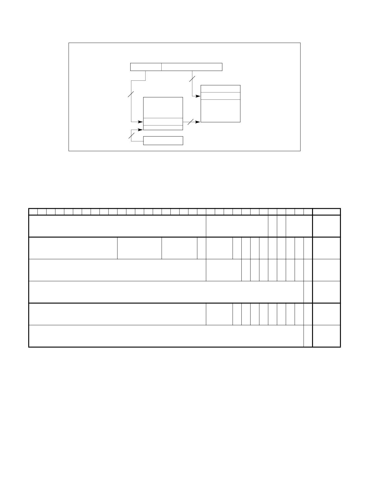
PAGING
Linear Address
31
22 21
0
Directory
Offset
22
4-MByte Page
Page Directory
10
Physical Address
PDE with PS=1
18
32
CR3
Figure 4-3. Linear-Address Translation to a 4-MByte Page using 32-Bit Paging
Figure 4-4 gives a summary of the formats of CR3 and the paging-structure entries with 32-bit paging. For the
paging structure entries, it identifies separately the format of entries that map pages, those that reference other
paging structures, and those that do neither because they are “not present”; bit 0 (P) and bit 7 (PS) are high-
lighted because they determine how such an entry is used.
31
30
29
28
27
26
25
24
23
22
21
20
19
18
17
16
15
14
13
12
11
10
9
8
7
6
5
4
3
2
1
0
P
P
Address of page directory1
Ignored
C
W
Ignored
CR3
D
T
P
P
P
U
R
PDE:
Bits 31:22 of address
Reserved
Bits 39:32 of
A
Ignored
G
1
D
A
C
W
/
/
1
4MB
of 4MB page frame
(must be 0)
address2
T
D
T
S
W
page
I
P
P
U
R
PDE:
Address of page table
Ignored
0
g
A
C
W
/
/
1
page
n
D
T
S
W
table
PDE:
Ignored
0
not
present
P
P
P
U
R
PTE:
Address of 4KB page frame
Ignored
G
A
D
A
C
W
/
/
1
4KB
T
D
T
S
W
page
PTE:
Ignored
0
not
present
Figure 4-4. Formats of CR3 and Paging-Structure Entries with 32-Bit Paging
NOTES:
1. CR3 has 64 bits on processors supporting the Intel-64 architecture. These bits are ignored with 32-bit paging.
2. This example illustrates a processor in which MAXPHYADDR is 36. If this value is larger or smaller, the number of bits reserved in
positions 20:13 of a PDE mapping a 4-MByte page will change.
Vol. 3A
4-11

PAGING
Table 4-3. Use of CR3 with 32-Bit Paging
Bit
Contents
Position(s)
2:0
Ignored
3 (PWT)
Page-level write-through; indirectly determines the memory type used to access the page directory during linear-
address translation (see Section 4.9)
4 (PCD)
Page-level cache disable; indirectly determines the memory type used to access the page directory during linear-
address translation (see Section 4.9)
11:5
Ignored
31:12
Physical address of the 4-KByte aligned page directory used for linear-address translation
63:32
Ignored (these bits exist only on processors supporting the Intel-64 architecture)
Table 4-4. Format of a 32-Bit Page-Directory Entry that Maps a 4-MByte Page
Bit
Contents
Position(s)
0 (P)
Present; must be 1 to map a 4-MByte page
1 (R/W)
Read/write; if 0, writes may not be allowed to the 4-MByte page referenced by this entry (see Section 4.6)
2 (U/S)
User/supervisor; if 0, user-mode accesses are not allowed to the 4-MByte page referenced by this entry (see Section
4.6)
3 (PWT)
Page-level write-through; indirectly determines the memory type used to access the 4-MByte page referenced by
this entry (see Section 4.9)
4 (PCD)
Page-level cache disable; indirectly determines the memory type used to access the 4-MByte page referenced by
this entry (see Section 4.9)
5 (A)
Accessed; indicates whether software has accessed the 4-MByte page referenced by this entry (see Section 4.8)
6 (D)
Dirty; indicates whether software has written to the 4-MByte page referenced by this entry (see Section 4.8)
7 (PS)
Page size; must be 1 (otherwise, this entry references a page table; see Table 4-5)
8 (G)
Global; if CR4.PGE = 1, determines whether the translation is global (see Section 4.10); ignored otherwise
11:9
Ignored
12 (PAT)
If the PAT is supported, indirectly determines the memory type used to access the 4-MByte page referenced by this
entry (see Section 4.9.2); otherwise, reserved (must be 0)1
(M-20):13
Bits (M-1):32 of physical address of the 4-MByte page referenced by this entry2
21:(M-19)
Reserved (must be 0)
31:22
Bits 31:22 of physical address of the 4-MByte page referenced by this entry
NOTES:
1. See Section 4.1.4 for how to determine whether the PAT is supported.
2. If the PSE-36 mechanism is not supported, M is 32, and this row does not apply. If the PSE-36 mechanism is supported, M is the min-
imum of 40 and MAXPHYADDR (this row does not apply if MAXPHYADDR = 32). See Section 4.1.4 for how to determine MAXPHY-
ADDR and whether the PSE-36 mechanism is supported.
4-12
Vol. 3A