Loongson 1C300 Processor User Manual (Version 1.0, 2014) - page 11
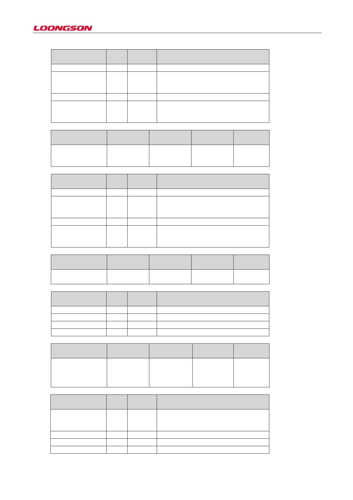
y_range
Bit
Default
Description
values
reserved
31:26
0x0
y_range_max
25:16
0x3ff
The maximum threshold of y direction is
used to judge whether the touch screen has
been pressed.
reserved
15:10
0x0
y_range_min
9:0
0x0
The minimum threshold of y direction is
used to judge whether the touch screen has
been pressed.
Register name
Address
Read / Write
Function
Reset value
(R / W)
description
awatchdog_range
0xbfe74018
r/w
Analog
0x3f0000f
watchdog
threshold
awatchdog_range
Bit
Default
Description
values
reserved
31:26
0x0
awcg_range_max
25:16
0x3f0
The maximum threshold of analog
watchdog is used to judge whether the
interrupt is generated.
reserved
15:10
0x0
awcg_range_min
9:0
0xf
The minimum threshold of analog
watchdog is used to judge whether the
interrupt is generated.
Register name
Address
Read / Write
Function
Reset value
(R / W)
description
axis
0xbfe74020
ro
Touch screen0x0
coordinates
axis
Bit
Default
Description
values
reserved
31:26
0x0
x_axis
25:16
0x0
X coordinate of the touch screen
reserved
15:10
0x0
y_axis
9:0
0x0
Y coordinates of the touch screen
Register name
Address
Read / Write (R
Function
Reset value
/ W)
description
adc_s_dout0
0xbfe74024
ro
Single
0x0
conversion
result, channel
0 and channel 1
adc_s_dout0
Bit
Default
Description
values
adc_busy
31
0x0
Switch to busy status and set the bit to 1
after writing soc. The hardware is cleared
after all single conversions.
reserved
30:26
0x0
adc_data1
25:16
0x0
Single conversion result of Channel 1
reserved
15:10
0x0
-198-
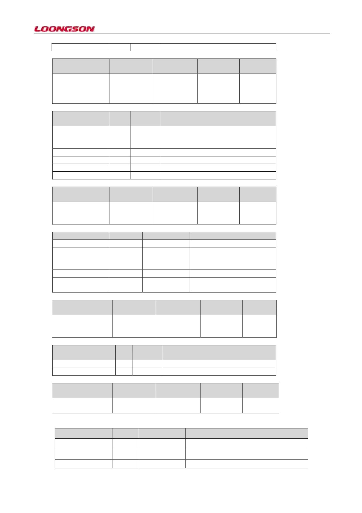
adc_data0
9:0
0x0
Single conversion result of Channel 0
Register name
Address
Read / Write (R
Function
Reset value
/ W)
description
adc_s_dout1
0xbfe74020
ro
Single
0x0
conversion
result, channel
0 and channel 1
adc_s_dout1
Bit
Default
Description
values
adc_busy
31
0x0
Switch to busy status and set the bit to 1
after writing soc. The hardware is cleared
after all single conversions.
reserved
30:26
0x0
adc_data3
25:16
0x0
Single conversion result of Channel 3
reserved
15:10
0x0
adc_data2
9:0
0x0
Single conversion result of Channel 2
Register name
Address
Read / Write (R
Function
Reset value
/ W)
description
adc_c_dout
0xbfe74028
ro
Continuous
0x0
conversion
results
adc_c_dout
Bit
Default values
Description
reserved
31:26
0x0
adc[i+1]
25:16
0x0
Conversion
results
of
ADC[i+1] in
continuous
conversion
reserved
15:10
0x0
adc[i]
9:0
0x0
Conversion results of ADC[i]
in continuous conversion
Register name
Address
Read / Write (R
Function
Reset value
/ W)
description
adc_debounce_cnt
0xbfe7402c
ro
Touch screen0x640
debouncing
time
adc_debounce_cnt
Bit
Default
Description
values
reserved
31:20
0x0
debounce_cnt
19:0
0x640
Debouncing delay time
Register name
Address
Read / Write (R
Function
Reset value
/ W)
description
adc_int
0xbfe74030
ro
ADC interrupt0x0
flag and control
Bit
Default values
Description
adc_int
reserved
31:10
0x0
fifo empty status in continuous conversion
fifo_empty
9
0x0
fifo_full_int_en
8
0x0
In continuous conversion, fifo full interrupt
-199-
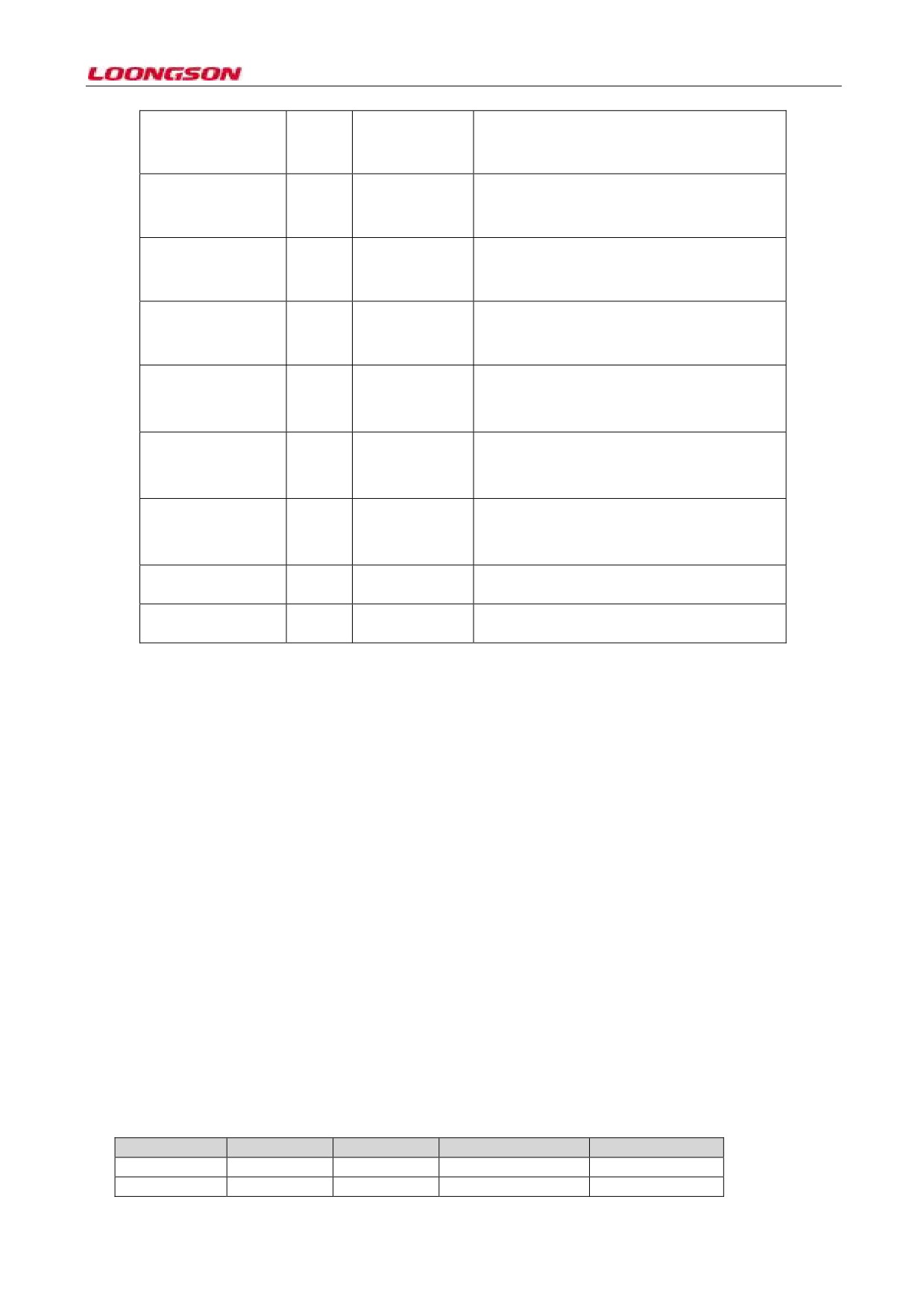
enable. When the bit is 1, the interrupt is
started; when the bit is 0, the interrupt is
masked.
awcg_int_en
7
0x0
Analog watchdog interrupt enable. When the
bit is 1, the interrupt is started; when the bit is
0, the interrupt is masked.
release_int_en
6
0x0
Touch screen released interrupt enable. When
the bit is 1, the interrupt is started; when the
bit is 0, the interrupt is masked.
press_int_en
5
0x0
Touch screen pressed interrupt enable. When
the bit is 1, the interrupt is started; when the
bit is 0, the interrupt is masked.
Fifo_full_int
4
0x0
In continuous conversion, fifo full interrupt
status, the software writes 1 and is cleared
0
awcg_h_int
3
0x0
The voltage of analog watchdog exceeds the
maximum threshold interrupt state, the
software writes 1 and is cleared
awcg_l_int
2
0x0
The voltage of analog watchdog exceeds the
minimum threshold interrupt state, the
software writes 1 and is cleared
Touch screen released interrupt status. The
release_int
1
0x0
software writes 1 and is cleared.
Touch screen pressed interrupt status. The
press_int
0
0x0
software writes 1 and is cleared.
24.3 Configuration Operations
Before the ADC interface works normally, configure all registers need configuring. The configuration procedures
of ADC controller are as follows:
1. Configure adc_int register, enable or disable the interrupt of ADC controller.
2. Configure time parameter register adc_cnt, set frequency division factor and interval of continuous conversion.
3. If there is touch screen application, configure adc_debounce_cnt, and set the pressed or released deboucing time;
in addition, thresholds in X and Y directions are configured to judge whether the interrupt is generated.
4. If there is analog watchdog application, configure the awatchdog_range register, and the watchdog threshold.
5. Configure adc_c_ctrl register, set the application mode (such as touch screen application and analog watchdo)
and continuous conversion channel.
6. Configure adc_s_ctrl register, set the single conversion channel, start and stop conversion.
7. Result-reading register. The single conversion result is stored in adc_s_dout0 and adc_s_dout1; the coordinates
of touch screen are stored in axis; the result of continuous conversion read adc_c_dout register via DMA.
Notes: after the continuous conversion starts, the conversion won’t stop unless adc_c_ctrl[7] is configured to 0. If
it’s necessary to change the continuous conversion channel, stop the continuous conversion first, and start the
conversion again after the reconfiguration of channels. If it’s necessary to insert the single conversion during
continuous conversion (the single conversion can’t be done in the used continuous conversion channel), and it’s
not necessary to stop the continuous conversion. The results of each continuous conversion will replace the
previous value, so the touch screen coordinates axis and adc_c_dout must be read promptly.
In addition, in general ADC continuous conversion, the corresponding relationship of channel selection and
adc_c_dout output is shown in the table below. For example, ch_c_sel[3:0]=b, select ADC0, ADC1 and ADC3
continuous conversion, the ADC0 data are put in adc_c_dout[9:0] of the first word, the ADC1 data put in
adc_c_dout[25:16] of the first word, and the ADC3 data put in adc_c_dout[9:0] of the second word.
ch_c_sel[3:0]
ch[0]
ch[1]
ch[2]
ch[3]
1
Dout0[9:0]
2
Dout0[9:0]
-200-
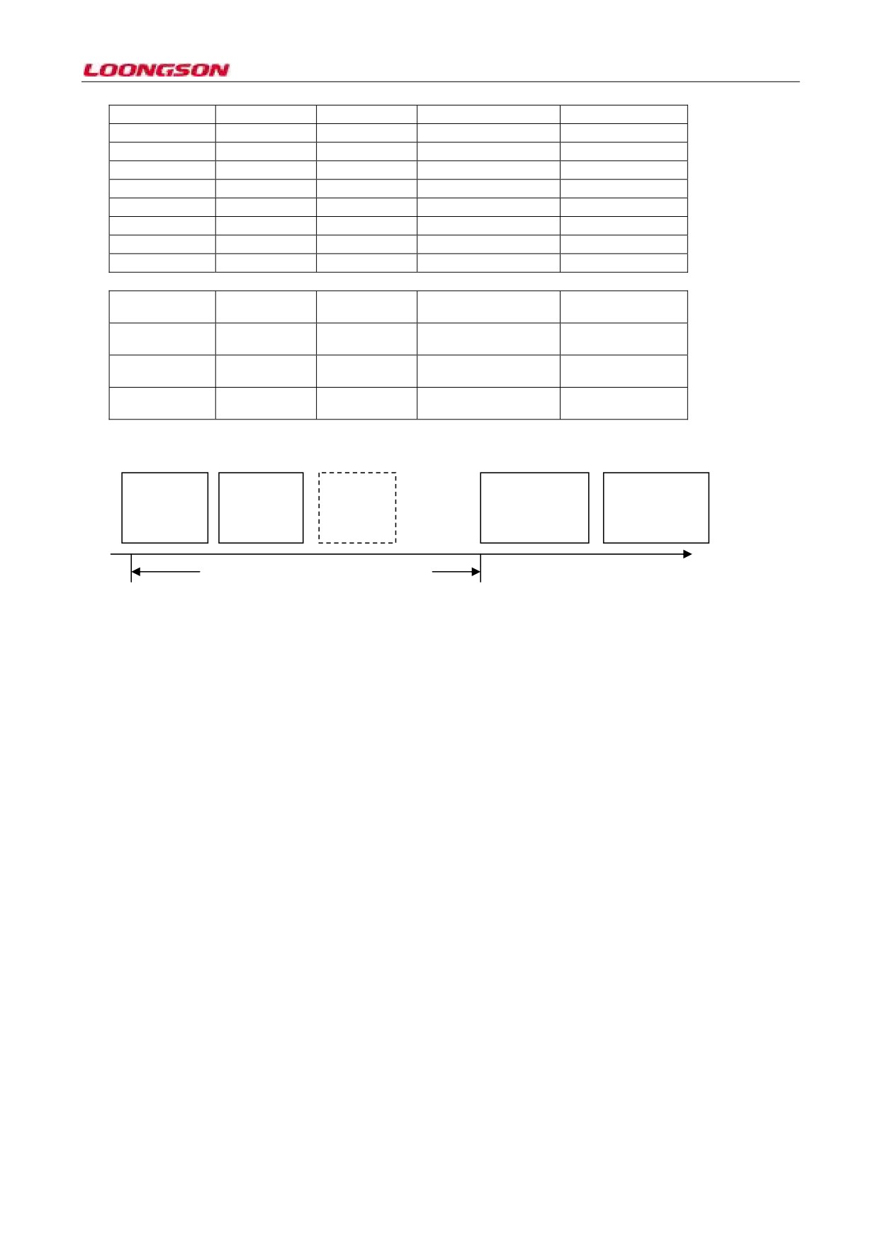
3
Dout0[9:0]
Dout0[25:16]
4
Dout0[9:0]
5
Dout0[9:0]
Dout0[25:16]
6
Dout0[9:0]
Dout0[25:16]
7
Dout0[9:0]
Dout0[25:16]
Dout1[9:0]
8
Dout0[9:0]
9
Dout0[9:0]
Dout0[25:16]
a
Dout0[9:0]
Dout0[25:16]
b
Dout0[9:0]
Dout0[25:16]
Dout1[9:0]
c)
Dout0[9:0]
Dout0[25:16]
d
Dout0[9:0]
Dout0[25:16]
Dout1[9:0]
e
Dout0[9:0]
Dout0[25:16]
Dout1[9:0]
f
Dout0[9:0]
Dout0[25:16]
Dout1[9:0]
Dout1[25:16]
The sequence diagram of inserting single conversion in continuous conversion is shown as follows:
Continuous
Continuous
If any
Next continuous
Next continuous
。。。
conversion
conversion
single
conversion
conversion
conversion
ch[i]
ch[i+1]
ch[i]
ch[i+1]
cc-gap
time
Figure 24-1 Schematic diagram of ADC single conversion/continuous conversion
If the cc_gap interval is not long enough for inserting one single conversion, it will cause the timing of the next
continuous conversion move backwards, which should be noted in software configuration of cc_gap.
-201-
25 PWM Controller
25.1 Overview
Loongson 1C has implemented the four-way pulse width adjustment/count controller (hereinafter referred to as
PWM), and each way of PWM work and control mode are the same. Each PWM has one way pulse width output
signal (pwm_o)). The system clock is up to 100MHz, and count register and parameter register are all 24bits data
width.
The base address of the four-way PWM controller system is shown as follows:
Table 25-1 Four-channel controller description
Name
Base address
PWM0
0xbfe5_c000
PWM1
0xbfe5_c010
PWM2
0xbfe5_c020
PWM3
0xbfe5_c030
Each way of controller has four control registers in total as follows:
Table 25-2 Control register description
Name
Address
Width
Access
Note
CNTR
Base + 0x0
24
R/W
Basic counter
HRC
Base + 0x4
24
R/W
High
pulse
timing
reference register
LRC
Base + 0x8
24
R/W
Low
pulse
timing
reference register
CTRL
Base + 0xC
8
R/W
Control register
25.2 PWM Register Description
Implement pulse width function
CNTR register can be written in by system programming to obtain the initial value, and after the system
programming and writing, driven by system clock CNTR register will add continuously, and is cleared after
reaching the value of LRC register. Then, it will start to add continuously, and the controller produces the
continuous pulse width output.
Table 25-3 Basic counter settings
CNTR
Bit field
Access
Reset value
Note
Reserved
31:24
R/W
0x0
CNTR
23:0
R/W
0x0
Basic counter count value. After
the counter starts to work
(CTRL[0] is 1), after counted to
Lvalue, the counter is cleared. If
CTRL[4] is 0, the counter starts
to count from start; if CTRL[4] is
1, the counter stops.
HRC register is written in by system, and when the value of CNTR register is equal to HRC value, controller
generates high level pulse.
Table 25-4 High pulse count threshold settings
Hvalue
Bit field
Access
Reset value
Note
Reserved
Hvalue
23:0
R/W
0x0
High pulse count threshold.
-202-

When the counter counts to the
threshold, output high level (it’s
necessary to configure CTRL[3]
to 0)
LRC register is written in by system, and when the value of CNTR register is equal to LRC value, the controller
will generate low pulse level.
Table 25-5 Low pulse count threshold settings
Lvalue
Bit field
Access
Reset value
Note
Reserved
Lvalue
23:0
R/W
0x0
Low pulse count threshold.
When the counter counts to the
threshold, the low level is
output.
For example, if the width to be generated has been the high pulse width 50 times system clock cycle and low pulse
width 90 times system clock cycle. In HRC, the initial value should be configured as (90-1)=89, and in LRC
register, the initial value configured as (50+90-1)=139
When working in timer mode, CNTR records the internal system clock, and the initial value of HRC and LRC
registers are written in by system programming. When the value of CNTR register is equal to HRC or LRC, the
chip will generate an interrupt, and the timer function is implemented thereby.
In three operating modes of CTRL control register, the function of control register remains unchanged, and
different configurations are selected based on functional requirement.
Table 25-6 Control register settings
CTRL
Bit field
Access
Reset value
Description
INT_LRC_EN
11
R/W
0
Low pulse counter interrupt enable
Set
1: when the INTEN is
1, the
interrupt is generated after the CNTR
counts to LRC.
Set to 0: no interrupt is generated
INT_HRC_EN
10
R/W
0
High pulse counter interrupt enable
Set 1, when the INTEN is 1, CNTR
an interrupt is generated after CNTR
counts to HRC,
Set to 0: no interrupt is generated
Reserved
9:8
R/W
0
CNTR_RST
7
R/W
0
Make CNTR counter clear
Set to 1: CNTR counter is cleared
Set
0: the CNTR counter works
normally
INT_SR
6
R/W
0
Interrupt status bit
Read operation:
1 represents that the
interrupt occurs;
0 represents no
interrupt
Write in 1: Clear interrupt
Interrupt enable bit
INTEN
5
R/W
0
Set 1: interrupt enable. Only when the
bit is
1 and meets the interrupt
conditions of high pulse or low pulse,
the interrupt occurs.
Set to 0: no interrupt is generated
SINGLE
4
R/W
0
Single pulse control bit
Set to 1: generate pulse only once
Set to 0: continue to generate pulse,
-203-

OE
3
R/W
0
pulse output enable control bit, active
low
Set to 0: pulse output enable
Set to 1: pulse output mask
Reserved
2: 1
R/W
2'b0
Reserved
CNT_EN
R/W
0
Basic counter enable bit
0
Set to 1: CNTR to count
Set to 0: CNTR stops counting
-204-
26 Watchdog (WDT)
26.1 Overview
In the system, the WDT (Watchdog Timer) is actually a counter. Generally, a large number is assigned to the
Watchdog, and the Watchdog starts to count down after the system runs. If the program works normally, later the
CPU should send out command to make the Watchdog reset and restart to count down. If the Watchdog reduces to
0, the program is considered to work abnormally, and the entire system is forced to reset. The figure below is the
implementation of Watchdog, and the system configuration of Watchdog. The Watchdog has one counter inside,
and the internal comparator compares if the counter value is zero. If it’s zero, it will send the soft reset signal to
restart the system.
Figure 26-1 Watchdog architecture chart
26.2 Description of WATCHDOG Register
The Watchdog logic mainly has three programmable registers, and the base address is Those formations are
described as follows:
26.2.1 Watchdog Enable Register (WDT_EN)
Address: 0xbfe7_c060
Bit
Bit field name
RW
Description
(read/write)
31:1
Reserved
0
WDT_EN
R/W
Watchdog enable
26.2.2 Watchdog Set Register (WDT_SET)
Address: 0xbfe7_c068
Bit
Bit field name
RW
Description
(read/write)
31:1
Reserved
0
WDT_SET
R/W
Watchdog counter setting
26.2.3 Watchdog Timer (WDT_timer)
Address: 0xbfe7_c064
-205-

Bit
Bit field name
RW
Description
31:0
WDT_timer
R/W
Watchdog counter value
The setup sequence of such three registers in system: the system first configures the Watchdog enable bit
WDT_EN; then, it configures the initial value of Watchdog starts timer WDT_TIMER, and the value has been
stored in a special register; after the system sets WDT_SET, the counter begins to count.
The Watchdog hasn’t implemented the function of low consumption, and its operation has nothing to do with the
hardware design. If the Watchdog is required to operate, the software needs to update the counter value timely.
-206-
27 High-precision Timer (HCNTR)
27.1 Overview
1C2 chip adds a high-precision timer inside, adopts 1M clock count, and may generate the cyclic interrupt output
by 1us at least and 231us at most based on configuration register. The timer clock is from external oscillator, and
isn’t affected by the chip operating frequency. When the system implements the dynamic undeclocking, it provides
the steady clock.
27.2 Register Description
Register name
Address
RW (read/write)
Function description
Reset value
hcntr_ctrl
0xbfe74028
r/w
CNTR control register
0x0
hcntr_ctrl
Bit
Default values
Description
cnt_en
31
0x0
Counter enable. When the bit is 1, the counter starts to count.
When the bit is 0, the counter stops counting
Reserved
30:5
0x0
int_prd
4:0
0x0
Timer interrupt period The interrupt cycle is 2int_prdus
Register name
Address
RW (read/write)
Function description
Reset value
hcntr_cntr
0xbfe74028
ro
CNTR counter value
0x0
hcntr_ctrl
Bit
Default values
Description
Reserved
31:20
0x0
hcntr_cntr
19:0
0x0
Timer count value for the current count
The timer can only implement the cycle timing by powers of 2, such as 1, 2, 4, 8 and16us. For example, if int_prd
is configured to 5, the interrupt cycle is 25=32us.
-207-