Loongson 1C300 Processor User Manual (Version 1.0, 2014) - page 8
14 General Purpose DMA
Loongson 1C processor includes a DMA module, and has three ways of DMA, which is used to operate block data
or stream data and enhance the working efficiency of processor. One IC chip has five modules (SDIO, ADC,
AC97, I2S, NAND), and will use the general DMA. Three ways of DMA are configured by software.
14.1 DMA Controller Structural Description
The process of DMA transferring data consists of three stages:
1. The pretreatment before transfer: the CPU finishes the following steps: configure the registers related to DMA
descriptor.
2. Data transfer: it is finished automatically under the control of DMA controller.
3. Transmission completion process: transmit an interrupt request.
The DMA controller is limited to the data transfer in the unit of byte (4 bytes). It designs the next descriptor
address register, source address register, destination address register, transfer data counter, transfer step-length
interval, transfer cycle index, DMA control logic, and other essential registers. The cache size of DMA is 128Byte
(32x4Byte) and is read in the unit of byte.
Through the configuration of DMA register, CUP saves the data from memory or equipment in cache memory, and
writes the data in buffer in the corresponding internal memory or equipment, and finally sends DMA end of
transmission signal. During the DMA transfer, the CPU can monitor the working condition of DMA at any time.
14.2 DMA Register
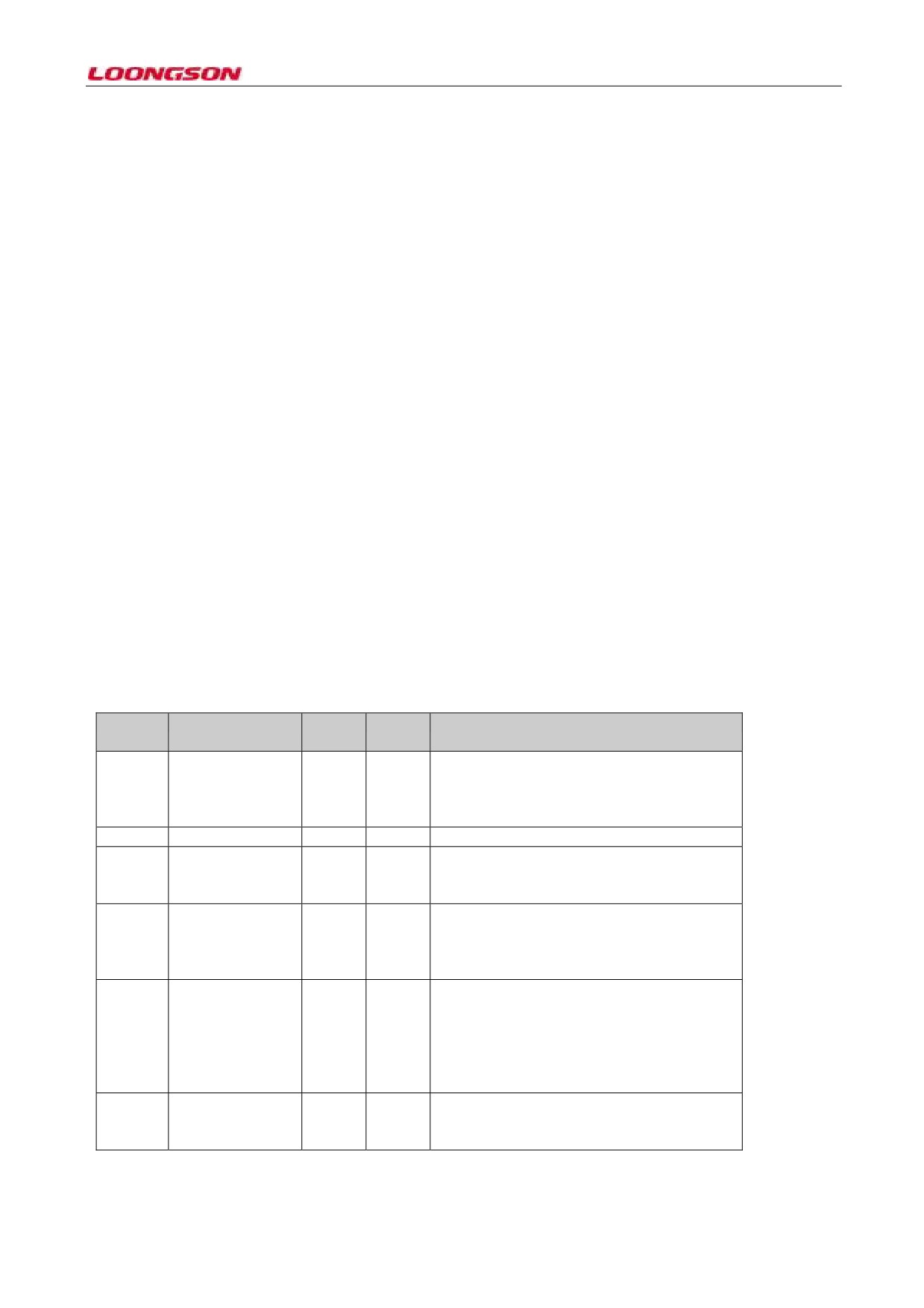
14.2.1ORDER_ADDR_IN
English name: this register is broadcast to the three-way DMA, and the selected DMA starts the work on the bit
width of register based on the register configuration. [31:0]
Address: 0xbfd0_1160
Reset value: 0x00000000
Bit field
Bit field name
Bit
Access
Description
width
31:6
Ask_addr
26
R/W
The high
26 bits and low
6 bits of first
descriptor address of the selected DMA are 0;
equivalently, the Ask_addr of 26 bits left shifts
6 bits.
5
Reserved
1
4
dma_stop
R/W
User request to stop the DMA operation;
1
Stop operation after the completion of current
data reading and writing operations
3
dma_start
1
R/W
It can start to read the first DMA descriptor of
descriptor chain;
When the register related to the first descriptor
is red back, this bit is reset.
2
Ask_valid
1
R/W
The user requests to write relevant information
of current DMA operation to the specified
memory address.
After the user writes backs relevant
information of DMA operation, this bit is
cleared.
1:0
Dev_num
2
R
2’b00 nand flash
2’b01 AC97 read device
2’b10 AC97 write device
Note:
-138-
The address of the first descriptor is in ORDER_ADDR_IN register, and the register is configured by CPU,
namely, Ask_addr lef shifts 6 bits and composes the base address of the descriptor register.
In each DMA operation, the address and significant bit of the next descriptor saved by DMA_ORDER_ADDR
register. If ask_valid=1, it indicates the CPU will monitor the DMA operation, and the value of DMA controller
register is written back to the memory directed by ask_addr.
If dma_start=1, it indicates the DMA operation starts. The DMA reads the descriptor from the memory address
directed by ask_addr, and starts to implement DMA operation based on descriptor information.
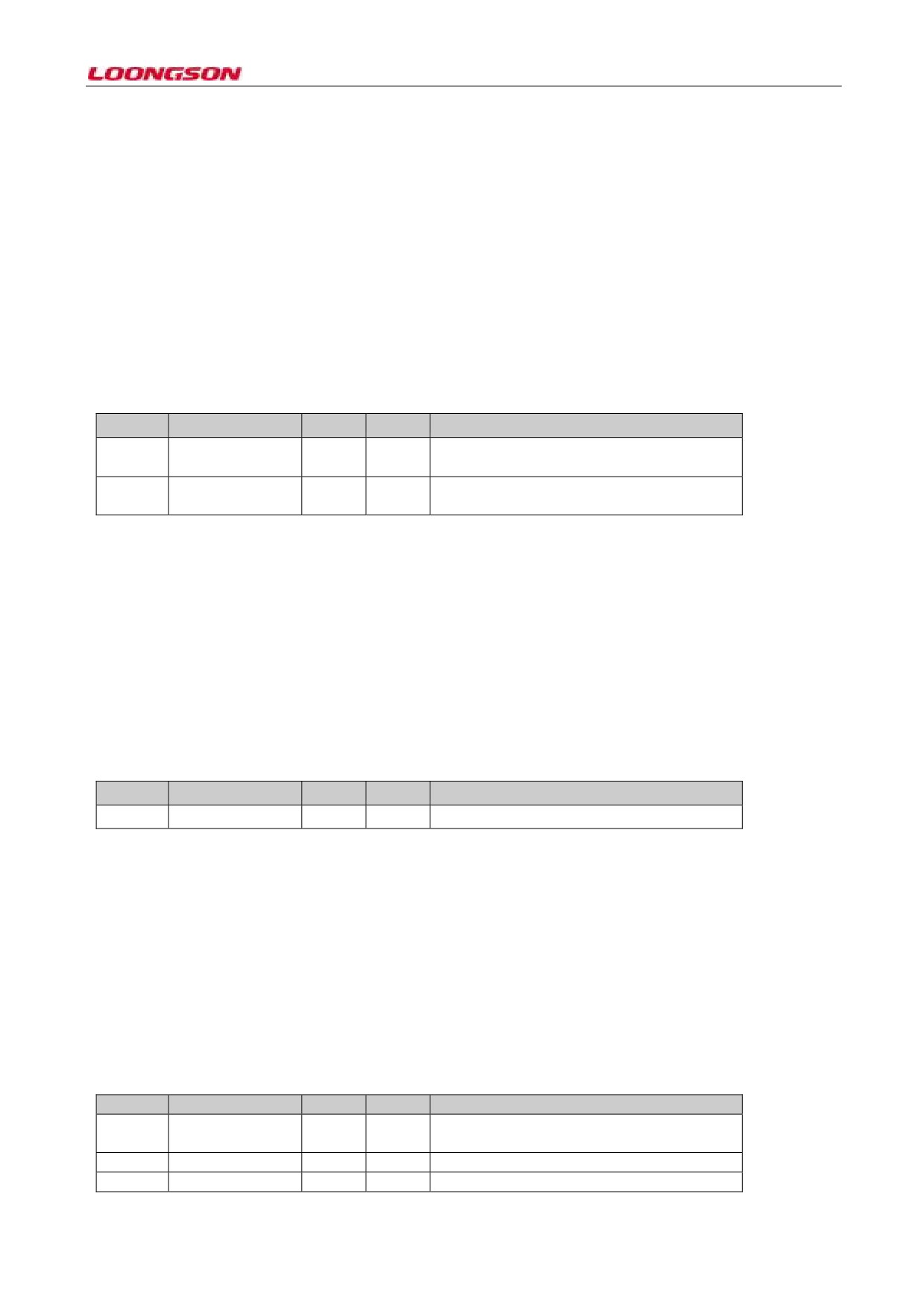
14.2.2DMA_ORDER_ADDR
English name: next descriptor address register
Register bit width: [31:0]
Base address: reset if the descriptor address is five bits lower.
Offset address: 0x0
Reset value: 0x00000000
Bit field
Bit field name
Bit width
Access
Description
31:1
dma_order_addr
31
R/W
Next descriptor address register of internal
memory
0
Dma_order_en
1
R/W
If descriptor is a valid signal
Notes: to store the address of the next DMA descriptor, dma_order_en is the enable bit of the next DMA descriptor.
If the bit is 1, it indicates the descriptor is valid, and if the bit is 0, it indicates the descriptor is invalid. Don’t
perform operation, and the address of 16 bytes is aligned. In the configuration of DMA descriptor, the register
stores the address of the next descriptor, and after the DMA operation is performed, determine whether to start the
next DMA operation by judging dma_order_en signal.
14.2.3DMA_SADDR
English name: memory address register
Register bit width: [31:0]
Base address: reset if the descriptor address is five bits lower.
Offset address: 0x4
Reset value: 0x00000000
Bit field
Bit field name
Bit width
Access
Description
31:0
dma_saddr
32
R/W
DMA operation memory address
Notes: the DMA operation is divided as follows: read the data from memory, and save them in the buffer of DMA
controller; the APB sends the request to access the data in DMA buffer, and the register specifies the address of
read memory; read the data from APB device, and save them in DMA buffer. When the number of words in DMA
buffer exceeds certain amount, the data will be written in memory, and the register has specified the address of
write memory
14.2.4 DMA_DADDR
English name: device address register
Register bit width: [31:0]
Base address: reset if the descriptor address is five bits lower.
Offset address: 0x8
Reset value: 0x00000000
Bit field
Bit field name
Bit width
Access
Description
31
1
R/W
AC97 write enables, “1” indicates the write
operation.
30
1
R/W
0: mono 1: 2 stero
29:28
2
R/W
AC97 write mode, 0: 1byte, 1: 2byte, 2: 4 byte
-139-
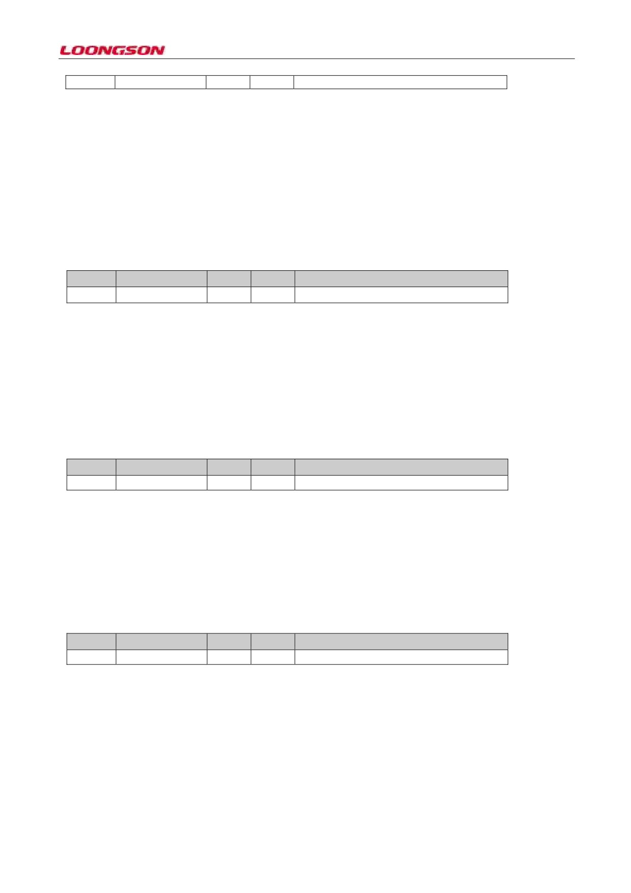
27:0
dma_daddr
32
R/W
APB device address in DMA operation
Notes: read the data from memory and save them in the buffer of DMA controller; the APB sends the request to
access the data in DMA buffer, and the register specifies the address of read memory; read the data from APB
device, and save them in DMA buffer. When the number of words in DMA buffer exceeds certain amount, the data
will be written in memory, and the register has specified the address of read APB device.
14.2.5 DMA_LENGTH
English name: length register
Register bit width: [31:0]
Base address: reset if the descriptor address is five bits lower.
Offset address: 0xc
Reset value: 0x00000000
Bit field
Bit field name
Bit width
Access
Description
31:0
dma_length
32
R/W
Transmission data length register
Notes: it represents the length of one block of transported content, and its unit is byte. After the length word is
transported, the next step starts, namely, next cycle. A new cycle starts, and the length word is transported again.
When the step becomes 1, the single DMA descriptor operation ends, and it starts to read the next descriptor.
14.2.6DMA_STEP_LENGTH
English name: interval length register
Register bit width: [31:0]
Base address: reset if the descriptor address is five bits lower.
Offset address: 0x10
Reset value: 0x00000000
Bit field
Bit field name
Bit width
Access
Description
31:0
dma_step_length
32
R/W
Data transmission interval length register
Notes: the interval lengths indicates the length between two transported memory data blocks, and the interval
between the end address of the previous step and the start address of the next step.
14.2.7DMA_STEP_TIMES
English name: cycle index register
Register bit width: [31:0]
Base address: reset if the descriptor address is five bits lower.
Offset address: 0x14
Reset value: 0x00000000
Bit field
Bit field name
Bit width
Access
Description
31:0
dma_step_times
32
R/W
Data transmission cycle index register
Notes: the cycle time indicates the number of blocks to be transported in one DMA operation. If it intends to
transport one continuous data block, the value of cycle time register is assigned 1.
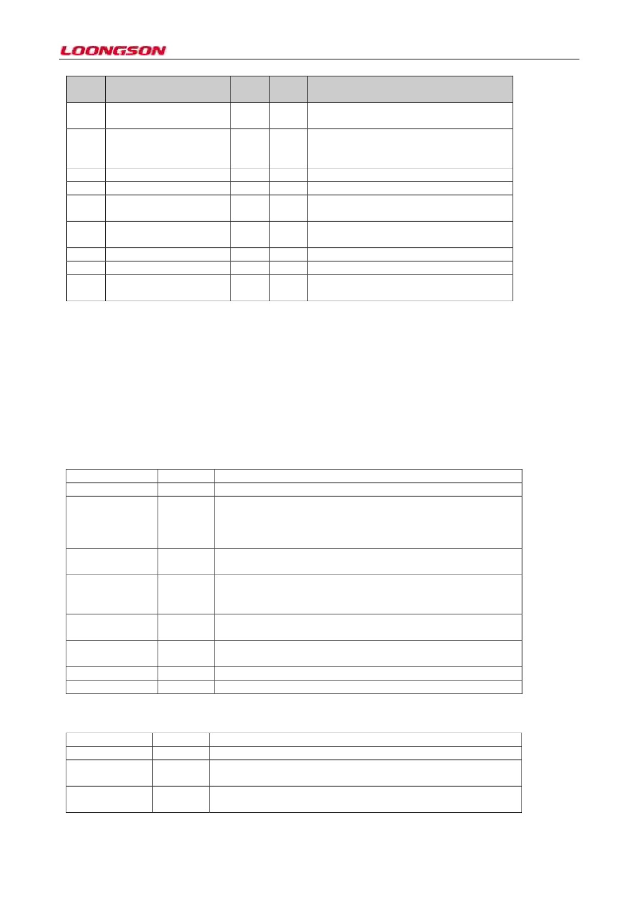
14.2.8 DMA_CMD
English name: control register
Register bit width: [31:0]
Base address: reset if the descriptor address is five bits lower.
Offset address: 0x18
Reset value: 0x00000000
-140-
Bit field
Bit field name
Bit
Access
Description
width
14:13
Dma_cmd
2
R/W
Generation types of source and destination
address
12
dma_r_w
1
R/W
DMA operation type, “1” is read memory
and write device,
“0” is read device and
write memory.
11:8
dma_write_state
4
R/W
DMA write data status
7:4
dma_read_state
4
R/W
DMA read data status
3
dma_trans_over
1
R/W
DMA implements the configured descriptor
operations.
2
dma_single_trans_over
1
R/W
Complete the implementation of one DMA
descriptor operation
1
dma_int
1
R/W
DMA interrupt signal
0
dma_int_mask
1
R/W
If DMA interrupts are masked out
Bit field
Bit field name
Bit
Access
Description
width
Notes: dma_single_trans_over=1 indicates that one DMA operation implementation finishes, and length=0 and
step_times=1, and it starts to pick up the descriptor of the next DMA operation. The descriptor address of the next
DMA operation is saved in DMA_ORDER_ADDR register, and if in DMA_ORDER_ADDR register
dma_order_en=0, dma_trans_over=1 and the entire dma operation finishes without new descriptor to read; if
dma_order_en=1, dma_trans_over is set to 0, and it starts to read the next dma descriptor. dma_int is the DMA
interrupt, and if without the interrupt mask, the interrupt occurs after one configured DMA operation finishes.
After the CPU deals with interrupt, it’s set to low directly. Equivalently, the DMA is automatically set low in next
transfer. dma_int_mask is the interrupt mask corresponding to dma_int. dma_read_state indicates the current read
state of DMA. dma_write_state indicates the current read state of DMA.
DMA write state (WRITE_STATE[3:0]) description, DMA includes the following write states:
Write_state
[3:0]
Description
Write_idle
4’h0
Idle writing status
W_ddr_wait
4’h1
Dma judgment needs to perform the operation of read device and
write memory, and sends the memory request. But when the
memory hasn’t prepared the response request, dma has been waiting
for the memory response.
Write_ddr
4’h2
The memory has received dma write request, but hasn’t performed
the write operation.
Write_ddr_end
4’h3
The memory receives dma write request, and finishes the write
operation, and then the dma is in the state of finishing the operation
of write memory.
Write_dma_wait
4’h4
Dma sends out the request of dma status register writes back to
memory, and waits for the memory to receive request.
Write_dma
4’h5
The memory receives the request of write dma status, but the
operation hasn’t finished.
Write_dma_end
4’h6
Memory completing writing dma status operation
Write_step_end
4’h7
Dma finishes one length operation (namely, one step)
DMA write state (WRITE_STATE[3:0]) description, DMA includes the following read states:
Read_state
[3:0]
Description
Read_idle
4’h0
Idle read status
Read_ready
4’h1
Receive the start signal of starting dma operation, enters into the
read state, and starts to read descriptors.
Get_order
4’h2
It sends the request of reading descriptor to the memory, and waits
for the response of memory.
-141-

Read_order
4’h3
The memory receives the request of reading descriptor, and is
performing the read operation.
Finish_order_end
4’h4
Memory completing reading dma descriptor
R_ddr_wait
4’h5
Dma sends the request of reading data to the memory, and waits for
the response of memory.
Read_ddr
4’h6
The memory receives the request of dma read data, and is
performing the read operation.
Read_ddr_end
4’h7
The memory finishes the one request of read data of dma
Read_dev
4’h8
Dma into the reading device status
Read_dev_end
4’h9
The device returns the read data, and ends the request of reading the
device.
Read_step_end
4’ha
After one step operation is finished, step times decrease 1.
14.3 Multiple Modules Use DMA Configuration Description
If some module needs to perform DMA operation, it needs to send the request to req signal of DMA. Through the
configuration of misc_ctrl register, only after the req signal of this module is connected to req[2:0] signal of DMA,
the DMA can be used normally.
Therein, the priority of SDIO is the highest, and can be configured to any way among three channels; when SDIO
doesn’t use the 0 channle, NAND uses 0 channel; when SDIO doesn’t use the 1st channel, I2S and AC97 multiplex
the 1st channel; when SDIO doesn’t use the 2nd channel, ADC, 2S and AC97 multiplex the 2nd channel. ADC
priority is higher than I2S and AC97
DMA multiplexes the configuration corresponding to misc_ctrl[25:22]. Therein, misc_ctrl[22] is adc_dma_en,
misc_ctrl[24:23]is sdio_dma_en, misc_ctrl[25]为 ac97_en.
For example, SDIO uses the 1st channel, ADC the 2nd channel, NAND the 0 channle, it should be configured as
follows:
sdio_dma_en is 2, adc_dma_en is 1, ac97 and I2S can’t use DMA.
For example, SDIO uses the Channel 0, ADC the 2nd channel, I2S the 1st channel, it should be configured as
follows:
sdio_dma_en is 1, adc_dma_en is 1, ac97_en is 0.
-142-
15 SPI0 Controller
Serial peripheral equipment interface SPI bus technology is a full duplex, synchronous and serial data interface
standard between several types of microprocessors, microcontrollers and peripheral equipment launched by
Motorola company.
15.1 SPI Controller Architecture
The SPI controller integrated can only act as the host and connect slave. In terms of the software, except several
IO registers, SPI controller has one section mapped to the read-only memory space of SPI Flash. If this section of
memory space is allocated in 0xbfc00000, after reset it can be accessed directly without software intervention, so
as to support processor startup from SPI Flash. The base address of IO register of SPI is 0xbfe8_0000, and the
external storage address space is 0xbd00_0000 -0xbd7f_ffff, 8MB in total.
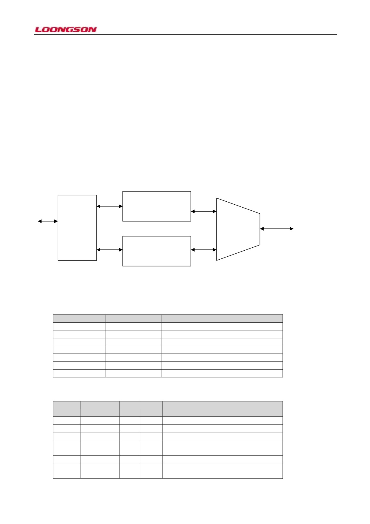
Its architecture is shown in Figure 15-1, and consists of AXI internal bus interface, simple SPI master controller,
SPI Flash read engine, and bus selection modules. Based on access address and type, the legal request from
internal bus interface is forward to SPI master controller or SPI Flash read engine
(the illegal request is
abandoned).
SPI
Main controller
AXI
SPI
interfaces
Seleted
bus
SPI FLASH
Reading engine
Figure 15-1 SPI controller architecture
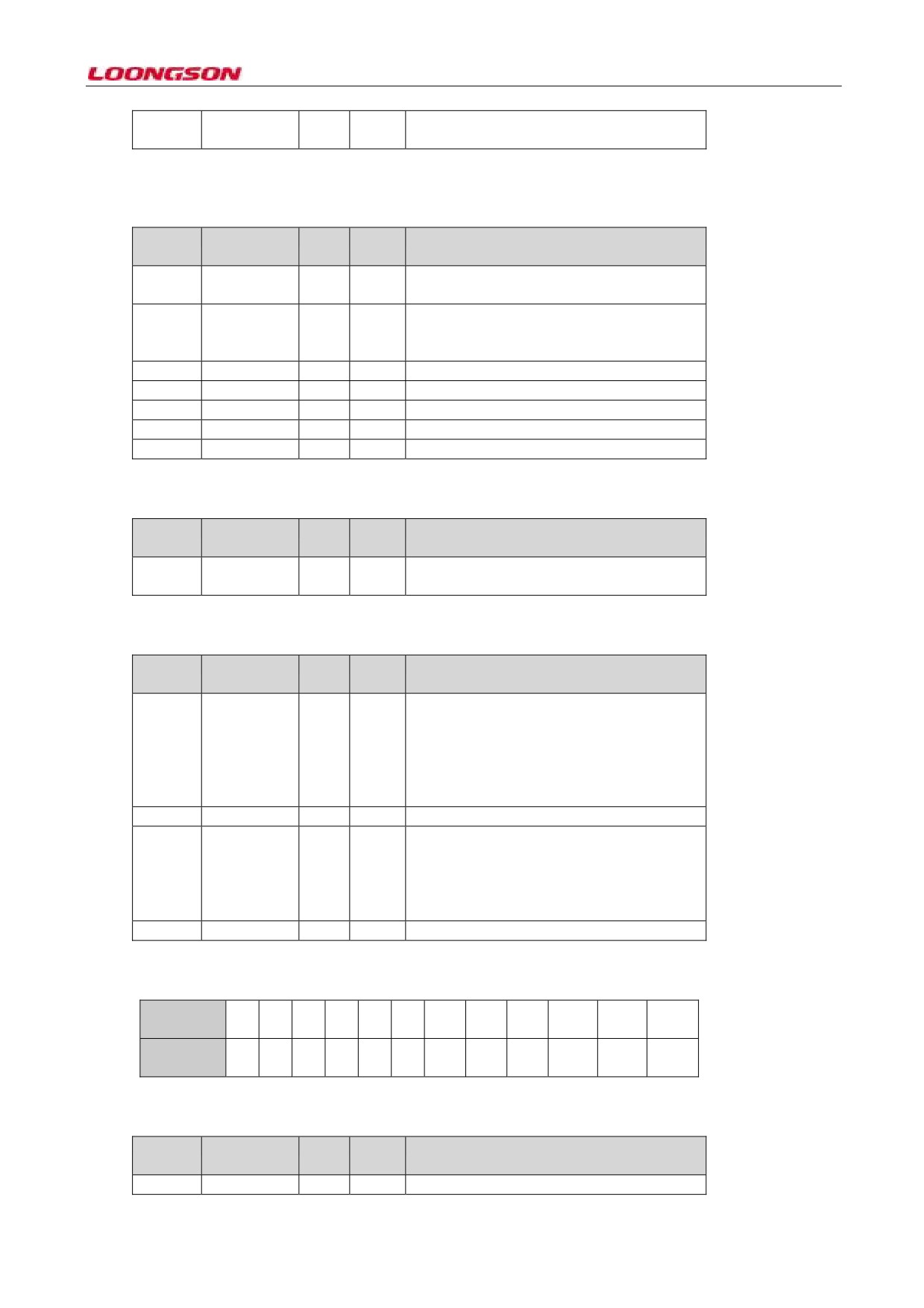
15.2 Configuration Register
Offset
Name
Description
0
SPCR
Control register
1
SPSR
Status register
2
TxFIFO/RxFIFO
DR (data register)
3
SPER
Internal register
4
SFC_PARAM
Parameter control register
5
SFC_SOFTCS
Chip selection control register
6
SFC_TIMING
Sequence control register
15.2.1 Control register (SPCR)
Bit field
Name
Access
Initial
Description
value
7
spie
R/W
0
Interrupt output enable signal active high
6
spe
R/W
0
System work enable signal active high
5
-
-
0
Reserved
4
mstr
-
1
Master mode selects the bit, and the bit
remains at 1.
3
cpol
R/W
0
Clock polarity bit
2
cpha
R/W
0
If the clock phase bit is
1, the phase is
opposite, and if it is 0, the phase is the same.
-143-
1:0
spr
R/W
0
sclk_o frequency division setup needs to be
used with spre of sper together.
15.2.2 Status register (SPSR)
Bit field
Name
Access
Initial
Description
value
7
spif
R/W
0
The interrupt flag bit 1 indicates that there is
interrupt request, write 1 and reset.
6
wcol
R/W
0
When the write register overflow flag bit is 1,
it indicates that it has overflowed, write 1 and
reset.
5:4
-
-
0
Reserved
3
wffull
R
0
Write register full flag 1 indicating full
2
wfempty
R
1
Write register empty flag 1 indicating empty
1
rffull
R
0
Read register full flag 1 indicating full
0
rfempty
R
1
Read register empty flag 1 indicating empty
15.2.3 Data register (TxFIFO/RxFIFO)
Bit field
Name
Access
Initial
Description
value
7:0
TxFIFO
W
-
Data transmission port
RxFIFO
R
Data receiving port
15.2.4 External register (SPER)
Bit field
Name
Access
Initial
Description
value
7:6
icnt
R/W
0
Transmit interrupt after several bytes
transmission
00: 1
01: 2
10: 3
11: 4
5:3
-
-
-
Reserved
2
mode
R/W
0
spi interface mode control
0: Sample simultaneous with the transmission
opportunity
1: Stagger half period of sampling and
transmission opportunity
1:0
spre
R/W
0
Set fractional frequency ratio with spr
Table 15-1 SPI frequency division factor
spre spr
00
00
00
00
01
01
01
01
10
10
10
10
00
01
10
11
00
01
10
11
00
01
10
11
Frequency
2
4
16
32
8
64
128
256
512
1024
2048
4096
coefficient
15.2.5 Parameter control register (SFC_PARAM)
Bit field
Name
Access
Initial
Description
value
7:4
clk_div
R/W
2
Clock frequency selection
-144-
Frequency division factor and
{spre, spr}
combination are the same.
3
dual_io
R/W
0
Dual I/O mode, the priority is higher than
quick read.
2
fast_read
R/W
0
Quick reading mode
1
burst_en
R/W
0
SPI flash supports the continuous address
read mode
0
memory_en
R/W
1
SPI flash read enables, if invalid, csn[0] can
be controlled by software.
Notes: when programmed to SPI flash via EJTAG, it needs to set memory_en to 0.
15.2.6 Chip selection control register (SFC_SOFTCS)
Bit field
Name
Access
Initial
Description
value
7:4
csn
R/W
0
csn pin-out output value
3:0
csen
R/W
0
When the bit is 1, the csn line corresponding
to the bit is controlled by 7:4 bit
15.2.7 Timing sequence control register (SFC_TIMING)
Bit field
Name
Access
Initial
Description
value
7:3
-
-
-
Reserved
2
tFAST
R/W
0
SPI flash read sampling mode
0: Along the sampling, interval of half SPI
period
1: Along the sampling, interval of one SPI
period
1:0
tCSH
R/W
3
The shortest invalid time of the chip selection
signal of SPI Flash is calculated by the clock
cycle T after frequency division
00: 1T
01: 2T
10: 4T
11: 8T
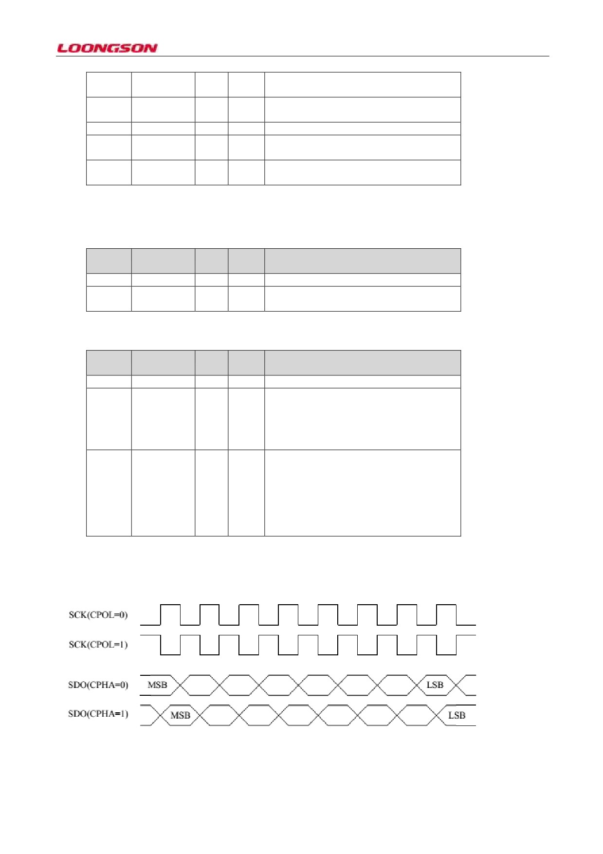
15.3 Interface Time Sequence
15.3.1 Timing sequence of SPI Master controller interface
Figure 15-2 Timing sequence of SPI Master controller interface
15.3.2 SPI Flash access timing sequence
-145-
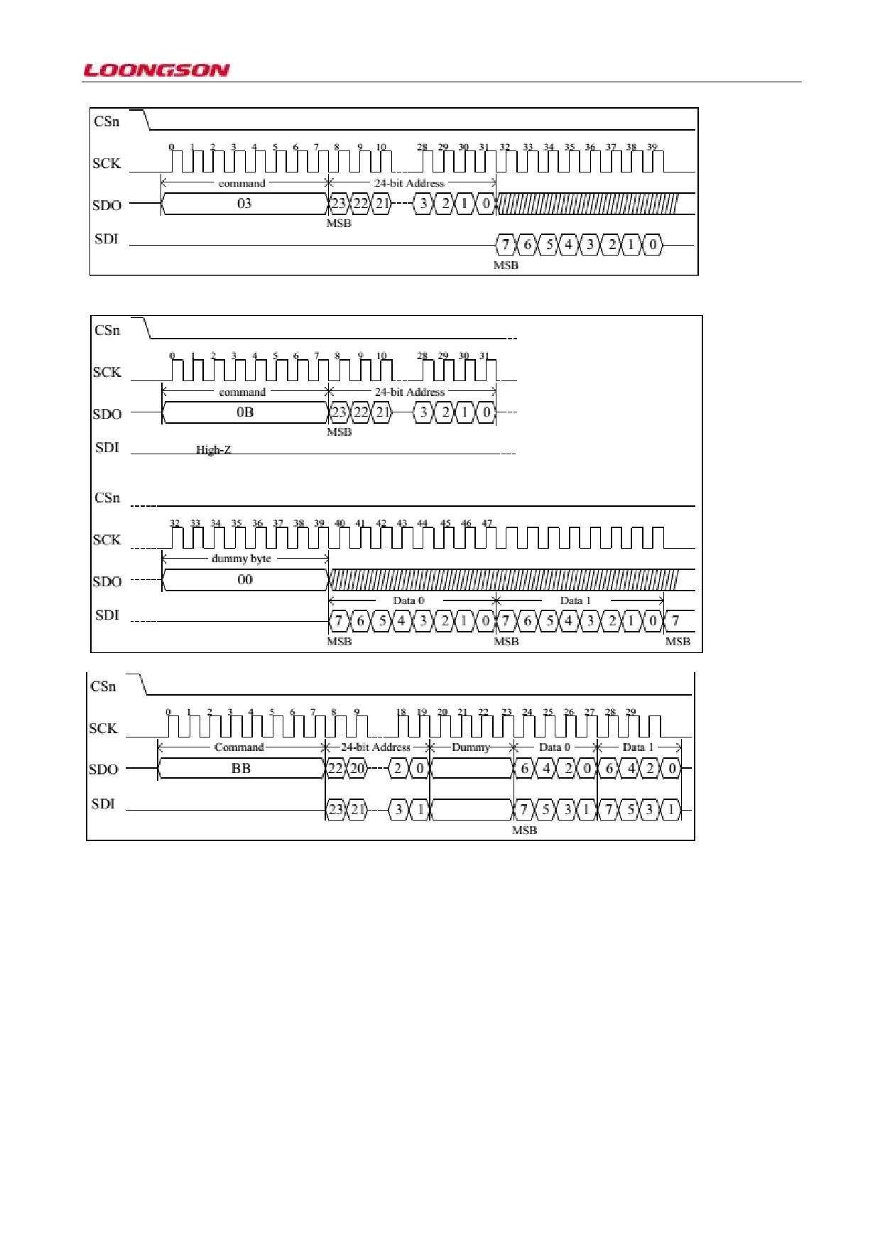
Figure 15-3 SPI Flash standard read timing sequence
Figure 15-4 SPI Flash rapid read timing sequence
Figure 15-5 SPI Flash directional I/O read timing sequence
15.4 User's Manual
15.4.1 Read and write operations of SPI master controller
1. Module initialization
Ɣ Stop SPI controller work, write 0 to the spe bit of control register spcr
Ɣ Reset state register spsr, write 8'b1100_0000 to register
Ɣ Set the external register sper, including the condition for interrupt request sper[7:6] and frequency division
factor sper[1:0]. Refer to register introduction.
Ɣ The configuration of SPI timing sequence includes the cpol and cpha of spcr, and mode bit of sper. When the mode
is 1, it’s the standard SPI implementation, and when the mode is 0, it’s the compatible mode.
Ɣ Configuration interrupt enable, the spie bit of spcr
-146-
Ɣ Start SPI controller, and write 1 to spe bit of control register spcr
2. Module transmission / transfer operations
Ɣ Write data in the data transmission register
Ɣ After the transmission finishes, read the data from the data transfer register. Because the transmission and receipt
happen simultaneously, even if SPI hasn’t sent effective data from the equipment, the read operation must be
performed.
3. Interrupt processing
ƔReceive the interrupt request
Ɣ Read the data of status register spsr, if spsr[2] is 1, it indicates the data transmission has finished, and if spsr[0]
is 1, it indicates it has received the data.
ƔRead or write data transmission register
ƔWrite 1 to spif bit of status register spsr, and clear the interrupt request of the controller
15.4.2 Hardware SPI flash head
1. Initialization
Ɣ Write 1 to the memory_en bit of SFC_PARAM. When the SPI is choosen as the starting device, this bit is reset
to 1.
Ɣ Set read parameters (clock frequency division, continuous address read, quick read, dual I/O, tCSH, etc.) These
parameter reset values are the most conservative.
2. Change the parameters
If the used SPI Flash supports higher frequency or provides the enhancement, the access speed of Flash can be
quickened greatly by modifying corresponding parameters. The parameter modification doesn’t need to close SPI
Flash read enable (memory_en)). Specific reference register instructions.
15.4.3 Mixed access to SPI Flash and SPI master controller
ƔAccess SPI Flash except read
After SPI Flash read enable shuts down, the software can directly control csn[0], and access SPI bus via SPI
master controller. It means that when performing this operation, instructins can’t be fetched from SPI Flash.
Except read, SPI Flash has implemented many commands (for example, erasion and write in), please refer to
relevant Flash files.
-147-
16 SPI1 Controller
Serial peripheral equipment interface SPI bus technology is a full duplex, synchronous and serial data interface
standard between several types of microprocessors, microcontrollers and peripheral equipment launched by
Motorola company.
16.1 SPI Master Controller Architecture
The implementation of SPI1 and SPI0 is the same, and the system start address won’t be mapped to SPI1
controller, so SPI1 doesn’t support system start. The base address of IO register of SPI1 is 0xbfec0000, and the
external storage address space of SPI1 is 0xbe00,0000 -0xbe3f,ffff, 4MB in total. Please refer to Chapter 15
information for all architectures and configurations
-148-
17 AC97 Controller
17.1 Overview (1C2 does not have this module)
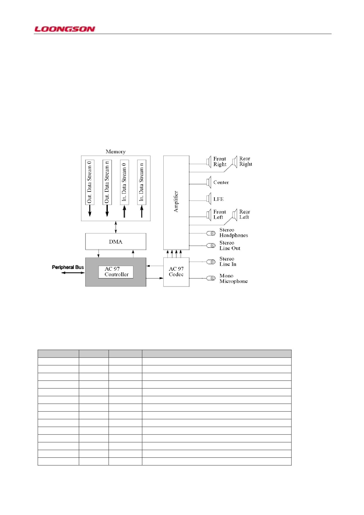
One AC97 application system in system is as shown in Figure 19-1. In one system on chip, three parts are
connected with AC97 controller: frstly, the peripheral bus to receive the control information and configuration
from microprocessor; secondly, AC97 Codec, multimedia digital signal coder decode that modulates PCM signal,
outputs the analogue voice received by human ears or convert the real sound to PCM singal; the conversion is
implemented via D/A convertor; thirdly, DMA engine, DMA is configured by microprocessor, and transports the
data from the memory area set by processor to FIFO or transports the data from FIFO to the set memory area.
Figure 17-1 AC 97 application system
17.2 AC97 Controller Register
The base address of the physical address of this module register is 0xbfe6_0000.
Register name
Width
Offset
Description
CSR
2
0x00
Configuration status register
OCC0
24
0x04
Output channel configuration register 0
OCC1
24
0x08
Reserved
OCC2
24
0x0C
Reserved
ICC
24
0x10
Input channel configuration register
CODEC_ID
32
0x14
Codec ID register
CRAC
32
0x18
Codec register access command
OC0
20
0x02
Output sound track 0
OC1
20
0x24
Output sound track 1
OC2
20
0x28
Reserved
OC3
20
0x2c
Reserved
OC4
20
0x30
Reserved
OC5
20
0x34
Reserved
OC6
20
0x38
Reserved
-149-
OC7
20
0x3c
Reserved
OC8
20
0x40
Reserved
IC0
20
0x44
Reserved
IC1
20
0x48
Reserved
IC2
20
0x4c
Input sound track 2
INTRAW
32
0x54
Interrupt status register
INTM
32
0x58
Interrupt mask
INTS
32
0x5c
Reserved
17.2.1 CSR register
English name: configuration status register
Register bit width: [31:0]
Offset: 0x00
Reset value: 0x00000000
Bit field
Bit field name
Bit width
Access
Description
31:2
Reserved
30
RO
Reserved
1
RESUME
1
R/W
Get suspended, read this bit and returns to the
state of the current AC97 subsystem.
1: AC97 suspend subsystem
0: normal working
In the suspended state, write 1 to this bit, and
start the recovery operation.
0
RST_FORCE
1
W
AC97 cold start
Write 1, and cause the cold start of AC97
Codec
17.2.2 OCC register
English name: output channel configuration register
Register bit width: [31:0]
Offset: 0x04
Reset value: 0x00004141
Bit field
Bit field name
Bit width
Access
Description
31:24
Reserved
8
R/W
Reserved
23:16
Reserved
8
R/W
Reserved
15:8
OC1_CFG_R
8
R/W
Output channel
1: right sound track
configuration
7:0
OC0_CFG_L
8
R/W
Output channel
0: left sound track
configuration
17.2.3 ICC register
English name: input channel configuration register
Register bit width: [31:0]
Offset: 0x10
Reset value: 0x00410000
Bit field
Bit field name
Bit width
Access
Description
31:24
Reserved
8
R/W
Reserved
23:16
IC_CFG_MIC
8
R/W
Input channel 2: MIC channel configuration.
15:8
Reserved
8
R/W
Reserved
-150-
7:0
Reserved
8
R/W
Reserved
The configuration format of sound channels in OCC and ICC registers are the same, namely,
OC0_CFG_L and OC0_CFG_R domains in OCC register and IC_CFG_MIC domain of OCC register in 17.2.3,
and the format of sound track is shown as follows:
Bit field
Bit field name
Bit
Access
Description
width
7
Reserved
1
R/W
Reserved
6
DMA_EN
1
R/W
DMA Enable
1: DMA Open
0: DMA Close
5:4
FIFO_THRES
2
R/W
FIFO threshold
5:4 Output channels input channels
00: FIFO 1/4 empty FIFO 1/4 full
01: FIFO 1/2 empty FIFO 1/2 full
10: FIFO 3/4 empty FIFO 3/4 full
11: FIFO fully empty FIFO fully full
3:2
SW
2
R/W
Sampling resolution
00:8 bit
10:16 Bit
1
VSR
1
R/W
Sampling rate
1: Variable sampling rate
0: Fixed sampling rate (48KHz)
0
CH_EN
1
R/W
Channel enable
1: Channel open
0: Channel shutdown (or enter a power-saving
status)
17.2.4 Codec register access command
English name: Codec register access command
Register bit width: [31:0]
Offset: 0x18
Reset value: 0x00000000
Bit field
Bit field name
Bit
Access
Description
width
31
CODEC_WR
1
R/W
Read / Write selection
1: read, when reading the data, set CODEC_WR to
read, and set the register address to be accessed in
CODEC_ADR; after returning to data complete
interrupt, reread value from CODEC_DAT register.
0: Write
30:23
Reserved
8
R
Reserved
22:16
CODEC_ADR
7
R/W
Codec register address
15:0
CODEC_DAT
16
R/W
Codec register data
17.2.5 Interrupt status register/interrupt mask register
English name: interrupt status / interrupt mask register
Register bit width: [31:0]
Offset: 0x54/58
Reset value: 0x00000000
Bit field
Bit field name
Bit width
Access
Description
-151-
31
IC_FULL
1
R/W
Input channel 2: FIFO full
30
IC_TH_INT
1
R/W
Input channel 2: FIFO threshold reached
29:8
Reserved
22
R/W
Reserved
7
OC1_FULL
1
R/W
Output channel 1: FIFO full
6
OC1_EMPTY
1
R/W
Output channel 1: FIFO empty
5
OC1_ TH_INT
1
R/W
Output channel 1: FIFO threshold reached
4
OC0_FULL
1
R/W
Output channel 0: FIFO full
3
OC0_EMPTY
1
R/W
Output channel 0: FIFO empty
2
OC0_ TH_INT
1
R/W
Output channel 0: FIFO threshold reached
1
CW_DONE
1
R/W
Codec register writing is completed
0
CR_DONE
1
R/W
Codec register read is completed
17.2.6 Interrupt status / clear register
English name: interrupt status / clear register
Register bit width: [31:0]
Offset: 0x 5c
Reset value: 0x00000000
Bit field
Bit field name
Bit width
Access
Description
31:0
INT_CLR
32
RO
The masked interrupt status register, the read
operation of this register will clear all interrupt
states in register 0x54
17.2.7 OC Interrupt clear register
English name: OC interrupt clear
Register bit width: [31:0]
Offset: 0x60
Reset value: 0x00000000
Bit field
Bit field name
Bit width
Access
Description
31:0
INT_OC_CLR
32
RO
The read operation of this register will clear
bit[7:2] corresponding to all output channel
interrupt states in register 0x54
17.2.8 IC Interrupt clear register
English name: IC interrupt clear
Register bit width: [31:0]
Offset: 0x64
Reset value: 0x00000000
Bit field
Bit field name
Bit width
Access
Description
31:0
INT_IC_CLR
32
RO
The read operation of this register will clear
bit[31:30] corresponding to all output channel
interrupt states in register 0x54
17.2.9 CODEC WRITE interrupt clear register
English name: CODEC WRITE interrupt clear
Register bit width: [31:0]
Offset: 0x68
Reset value: 0x00000000
Bit field
Bit field name
Bit width
Access
Description
-152-

31:0
INT_CW_CLR
32
RO
The read operation in this register will clear the
bit[1] in register 0x54
17.2.10 CODEC READ interrupt clear register
English name: CODEC READ interrupt clear
Register bit width: [31:0]
Offset: 0x 6c
Reset value: 0x00000000
Bit field
Bit field name
Bit width
Access
Description
31:0
INT_CR_CLR
32
RO
The read operation in this register will clear the
bit[0] in register 0x54
-153-
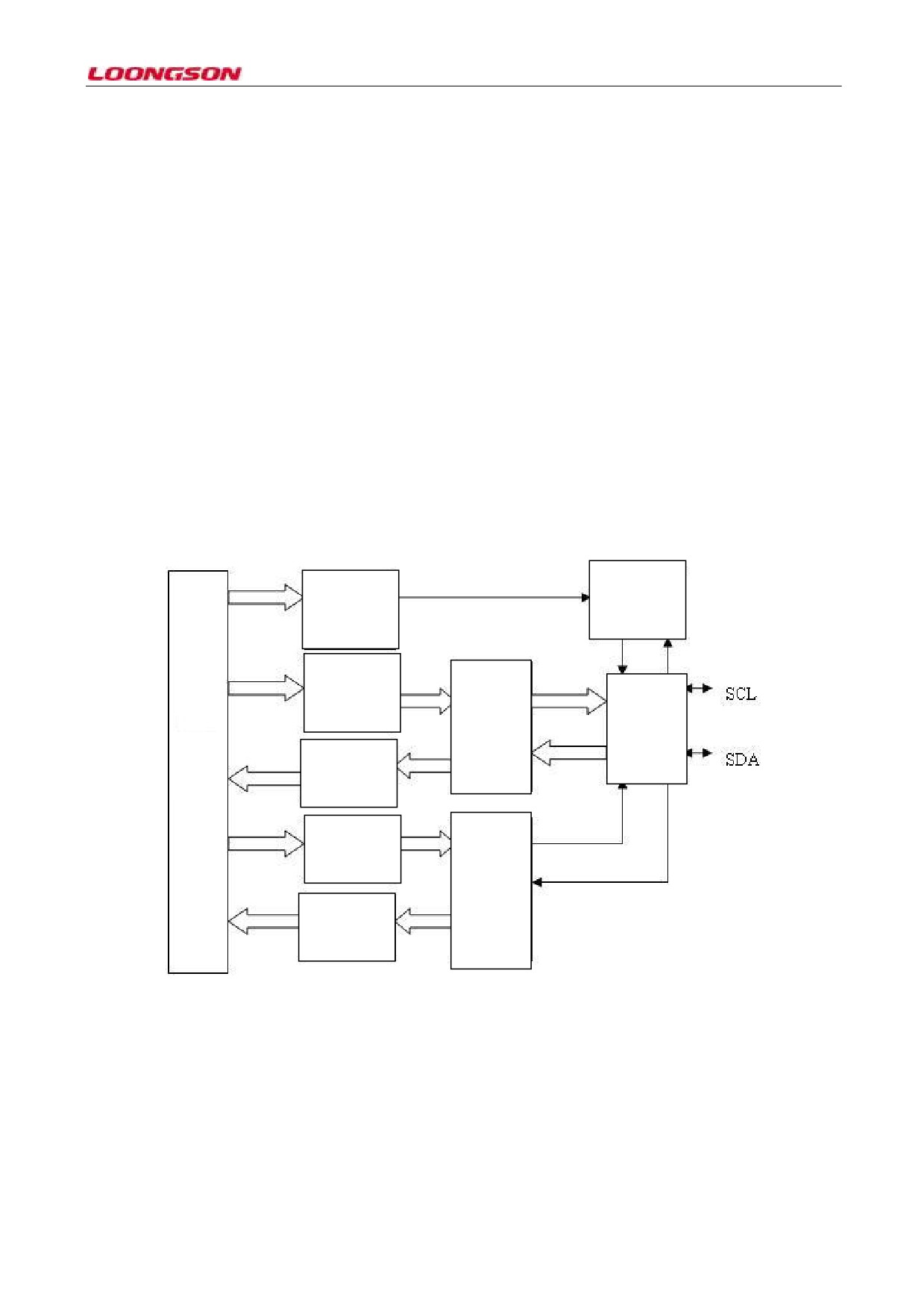
18 I2C Controller
18.1 Overview
This chapter has provided the details, configuration and use of I2C The chip in system integrates I2C interfaces,
and is mainly used to implement the data exchange between two devices. I2C bus is the serial bus consistuted by
data line SDA and clock SCL, and can send and receive data. The bidirectional transfer is conducted between
devices, Loongson 1C has integrated three-way I2C interfaces in total.
18.2 I2C Controller Architecture
Main modules of I2C master controller architecture include Clock Generator, Byte Command Controller, Bit
Command controller, and Data Shift Register. The rest are LPB bus interfaces and some registers.
Clock generator module: generate the frequency division clock, sync bit command. Byte command controller
module: interpret one command to the timing sequence of operation by bytes, namely, the byte operation is
decomposed into bit operation.
Bit command controller module: conduct the transmission of actual data, and the generation of bit command
signal.
Data shift register module: serial data shift
Clock
Frequency
generator
divider
register
CR
Byte
(command
Bit
comman
register)
comman
d
d
controll
Inter
controll
Status
er
face
er
register
Transmitte
Data
r register
shift
register
Receiving
register
Figure 18-1 I2C Master Controller architecture
18.3 I2C Controller Register Description
The base address of the physical address of I2C-0 module register is 0xbfe5_8000, and the address space is 16KB.
The base address of the physical address of I2C-1 module register is 0xbfe6_8000, and the address space is 16KB.
The base address of the physical address of I2C-2 module register is 0xbfe7_0000, and the address space is 16KB.
-154-
18.3.1 Frequency division latch low-byte register (PRERlo)
English name: frequency division latch low-byte register register bit width: [7:0]
Offset: 0x00
Reset value: 0xff
Bit field
Bit field name
Bit width
Access
Description
7:0
PRERlo
8
RW
Fractional frequency latch storage low 8
18.3.2 Frequency division latch high-byte register (PRERhi)
English name: Fractional frequency latch high byte register
Register bit width: [7:0]
Offset: 0x01
Reset value: 0xff
Bit field
Bit field name
Bit width
Access
Description
7:0
PRERhi
8
RW
Fractional frequency latch storage high 8
The frequency of frequency division clock clock_a in module is half of DDR_clk frequency (see Chapter 29 for
DDR_clk configuration); assuming that the value of frequency division latch is prescale, the output frequency of
SCL bus is clock_s (the clock is determined based on user’s demand and external I2C equipment characteristics),
and should meet the following conditions:
Prcescale=clock_a/(5*clock_s)-1
Or Prcescale=DDR_clk/(10*clock_s)-1
18.3.3 Control register (CTR)
English name: control register
Register bit width: [7:0]
Offset: 0x02
Reset value: 0x00
Bit field
Bit field name
Bit width
Access
Description
7
EN
1
RW
When the module wrok enable bit is 1, it’s the
normal operating pattern, and when it’s 0, the
frequency division register can operate.
6
IEN
1
RW
If interrupt enable bit is 1, open the interrupt
5:0
Reserved
6
RW
Reserved
18.3.4 Transmit data register (TXR)
English name: transmit register
Register bit width: [7:0]
Offset: 0x03
Reset value: 0x00
Bit field
Bit field name
Bit width
Access
Description
7:1
DATA
7
W
Store next byte to be transmitted
0
DRW
1
W
In data transfer, this bit saves the lowest bit of
the data; in address transfer, this bit indicates
read and write statuses
18.3.5 Receive data register (RXR)
English name: Receiving register
-155-
Register bit width: [7:0]
Offset: 0x03
Reset value: 0x00
Bit field
Bit field name
Bit width
Access
Description
7:0
RXR
8
R
Store the last received byte
18.3.6 Command control register (CR)
English name: Command register
Register bit width: [7:0]
Offset: 0x04
Reset value: 0x00
Bit field
Bit field name
Bit width
Access
Description
7
STA
1
W
Generate START signal
6
STO
1
W
Generate STOP signal
5
RD
1
W
Generate read signal
4
WR
1
W
Generate write signal
3
ACK
1
W
Generate acknowledge signal
2:1
Reserved
2
W
Reserved
0
IACK
1
W
Generate interrupt acknowledge signal
The hardware is automatically cleared after the I2C sends data. In bit read operartions, it’s always read back to ‘0’.
18.3.7 Status register (SR)
English name: Status register
Register bit width: [7:0]
Offset: 0x04
Reset value: 0x00
Bit field
Bit field name
Bit width
Access
Description
7
RxACK
1
R
Receive acknowledge bit
1 fail to receive acknowledge bit
0 receive acknowledge bit
6
Busy
1
R
I 2c Bus busy flag bit
1 busy bus
0 idle bus
5
AL
1
R
When I2C core loses I2C bus control right, this
bit is set to 1.
4:2
Reserved
3
R
Reserved
1
TIP
1
R
Indicate transmission process
1 indicate data is being transmitted
0 indicate data transmission is completed
0
IF
1
R
Interrupt flag bit, when one data transfer is
finished or another device initiates the data
transfer, this bit is set to 1.
-156-
19 UART Controller
19.1 Overview
IC integrates 12 UART controllers, and communicates via APB bus and bus bridge. UART controller provides the
function of serial communication with MODEM or other external equipment, for example, communicate with
another computer by serial links according to the standard of RS232. The controller design is well compatible with
international industrial standard semi-conductor equipment 16550A.
UART controller supports the expansion to USART mode by configuration register. The USART controller
complies with two basic protocols: T=0 and T=1 in ISO7816, and provides the support for infrared and smart card
interface modes.
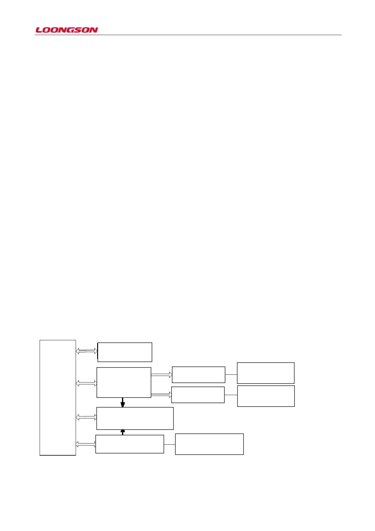
19.2 Controller Architecture
The UART controller has Transmitter and Receiver modules, MODEM module, Interrupt Arbitrator module, and
Register Access Control module, and their relationship is shown in the figure below. Main module functions and
features are described below:
Ɣ Transmitter and receiver modules: be responsible for sending and receiving the data frame. The transmitter module
converts the parallel data in FIFO transmit queue to serial data frame in the set form, and sends them through send
port. The receiver module monitors the signal in receiving end, and in case of significant start bit, it will receive
and convert the asyn serial data frame into parallel data, store them in FIFO receive queue, and check that the data
frame format is right. The frame structure of UART is set by line control register (LCR), and the status of
transmitter and receivers is stored in line control register (LCR).
Ɣ MODEM module: MODEM control register (MCR) controls the status of output signals DTR and RTS. MODEM
control module monitoring the line status of input signals DCD, CTS, DSR and RI, and record the state of those
signals in the bit corresponding to MODEM status register.
Ɣ Interrupt Arbitrator module: when any interrupt condition is met, and the corresponding bit of interrupt enable register
is set to 1, the interrupt request signal UAT_INT of UART is set to significant condition. In order to reduce the
interaction with external software, UART divides the interrupt into four grades, and identifies these interrupts in
interrupt identification register (IIR). The interrupt at four levels rank as follow is in the order of priority: receive
line status interrupt; receive data ready for interrupt; transfer the empty interrupt with register; MODEM status
interrupt.
Ɣ Access to register module: when UART module is selected, CPU can access to the register selected by address line by
read or write operations.
Frequency
divider
Receiver module
Access
to
Receive FIFO
interface
register module
Bus
Transmit FIFO
Transmit module
interface
interface
Interrupt
arbitration
module
MODEM register
MODEM interface
Figure 19-1 UART controller architecture
-157-