Loongson 1C300 Processor User Manual (Version 1.0, 2014) - page 1
Reading Guide
Loongson 1C300 Processor User's Manual mainly introduces the architecture and register of Loongson 1C300.
For more information about LS232 high-performance processor core integrated by Loongson 1C300, please refer
to Loongson LS232 Processor User Manual. Loongson 1C300 is hereinafter referred to as Loongson 1C.
Loongson Technology Corporation Limited
Revision history
Date
Edit
Version
Change
Mar. 14, 2013
R&D Centre
0.0.1
First draft
Jun. 16, 2013
R&D Centre
0.0.2
Supplement the description of DWT and interrupt
Mar. 29, 2013
R&D Centre
0.0.3
configuration register; revise the description of modules
such as CAMIF, UART and OTG.
Apr. 15, 2013
R&D Centre
0.1
Address space revision
Apr. 26, 2013
R&D Centre
0.2
Feb. 12, 2014
R&D Centre
0.3
Modify and typeset
Feb. 28, 2014
R&D Centre
0.9
Modify 1C2 changes after revision
Add the descriptions on pull-up/pull-down in the pin
Apr. 21, 2014
R&D Centre
1.0
Add the description of SRAM pin and revise some errors.
Chip name is updated as Loongson 1C 300
Loongson Technology Corporation Limited
’s Manual Content
Content
1 Overview
10
1.1 System Structure Chart
10
1.2 Main Functions of the Chip
10
1.2.1 Processor core
10
1.2.2 SDRAM Controller
11
1.2.3 SRAM/NOR FLASH Controller
11
1.2.4 NAND Controller
11
1.2.5 Clock generator
11
1.2.6 I2S controller
11
1.2.7 AC97 controller
11
1.2.8 LCD controller
11
1.2.9 Camera interface
11
1.2.10 MAC controller
12
1.2.11 USB2.0 controller
12
1.2.12 SPI controller
12
1.2.13 I2C controller
12
1.2.14 UART controller
12
1.2.15 GPIO
12
1.2.16 PWM controller
13
1.2.17 RTC
13
1.2.18 CAN controller
13
1.2.19 SDIO controller
13
1.2.20 ADC controller
13
2 Definition of Pin
14
2.1 Agreement
14
2.2 LCD Interface
14
2.3 SDRAM Interface
14
2.4 SRAM/NOR Flash Interface
15
2.5 I2S Interface
15
2.6 I 2C Interface
15
2.7 UART Interface
15
2.8 PWM Interface
16
2.9 ADC Interface
16
2.10 SPI Interface
16
2.11 EJTAG Interface
16
2.12 CAMERA Interface
17
2.13NAND Interface
17
2.14 MAC Interface
17
2.15 OTG Interface
17
2.16 USB Port
18
2.17 RTC Interface
18
2.18 Clock Configuration Signal
18
2.19 Power Ground
18
2.20 Initialization Signal
18
3 Register Definition
20
3.1 Base Register Definition
20
3.2 Each Module Register Definition
21
4 Clock Structure
26
4.1 Clock Architecture
26
4.2 Clock Signal Description
26
5 Chip Configuration and Control
27
5.1 Address space allocation
27
5.2 Chip Configuration Register (CONFREG)
28
5.2.1 PLL/SDRAM Frequency configuration register
28
5.2.2 CPU/CAMERA/DC frequency configuration register
28
I
Loongson Technology Corporation Limited
’s Manual Content
5.2.3 SDRAM parameter register
29
5.2.4 SHUT_CTRL register
30
5.2.5 MISC_CTRL register
31
5.2.6 cpu_throt register
31
5.2.7 UART multiplex configuration register
32
5.2.8 GPIO0 Configuration Register (corresponding GPIO[31:0])
33
5.2.9 GPIO1 configuration register (corresponding GPIO[63:32])
33
5.2.10 GPIO2 configuration register (corresponding GPIO[95:64])
34
5.2.11 GPIO3 configuration register (corresponding GPIO[127:96])
34
5.2.12 PAD[31:0] pin multiplex relation configuration register
34
5.2.13 PAD[63:32] pin multiplex relation configuration register
35
5.2.14 PAD[95:64] pin multiplex relation configuration register
36
5.2.15 PAD[127:96] pin multiplex relation configuration register
36
5.3 Interrupt Configuration Register
37
6 SDRAM Controller
42
6.1 Overview
42
6.2 Register Description
42
6.3 Software Configuration Description
42
6. CONFIG_VALID
43
7 SRAM Controller
44
7.1 Overview
44
7.2 Configuration Register
44
8 Camera Interface
45
8.1 Overview
45
8.2 Interface protocol
46
8.3 Register Description
47
8.4 Configuration Operations
49
8.4.1 Access memory mode
49
8.4.2 Configuration order
50
9 I2S Controller
51
9.1 Overview
51
9.2 Interface protocol
51
9.3 Dedicated Register
52
9.4 Configuration Operations
53
10 Display Controller (DC)
54
10.1 Overview
54
10.2 Register Definition and Description
54
10.2.1 Frame buffer configuration register
54
10.2.2 Frame buffer address register 0
54
10.2.3 Frame buffer address register 1
54
10.2.4 Frame buffer span register
54
10.2.5 Color dithering configuration register
55
10.2.6 Color vibrance lookup table low-bit register
55
10.2.7 Color dithering lookup table high-bit register
55
10.2.8 Color dithering description
55
10.2.9 LCD panel configuration register
56
10.2.10 Horizontal display width register
56
10.2.11 Line synchronization configuration register
56
10.2.12 Vertical display height register
56
10.2.13 Field synchronization configuration register
56
10.2.14 Output sequencing instructions
57
10.2.15 Gamma correction catalog register
57
10.2.16 Gamma correction value register
57
10.2.17 Gamma correction instructions
57
11 MAC Controller
59
11.1 DMA Register Description
59
II
Loongson Technology Corporation Limited
’s Manual Content
11.1.1 Register0 (Bus Mode Register)
59
11.1.2 Register2 (Receive Poll Demand Register)
60
11.1.3 Register2 (Receive Poll Demand Register)
60
11.1.4 Register3 (Receive Descriptor List Address Register)
60
11.1.5 Register4 (Transmit Descriptor List Address Register)
60
11.1.6 Register5 (Status Register)
60
11.1.7 Register0 (Bus Mode Register)
62
11.1.8 Register7 (Interrupt Enable Register)
64
11.1.9 Register8 (Missed Frame and Buffer Overflow Counter Register)
64
11.1.10 Register9(Receive Interrupt Watchdog Timer Register)
65
11.1.1 Register0 (Bus Mode Register)
65
11.1.12 Register11 (AXI Status Register)
66
11.1.13 Register18 (Current Host Transmit Descriptor Register)
66
11.1.14 Register19 (Current Host Receive Descriptor Register)
66
11.1.15 Register20 (Current Host Transmit Buffer Address Register)
66
11.1.16 Register21 (Current Host Receive Buffer Address Register)
67
11.2 MAC Controller Register Description
67
11.2.1 Register0 (MAC Configuration Register)
67
11.2.2 Register1 (MAC Frame Filter)
68
11.2.3 Register2 (Hash Table High Register)
69
11.2.4 Register3 (Hash Table Low Register)
69
11.2.5 Register4 (GMII Address Register)
69
11.2.6 Register5 (GMII Data Register)
70
11.2.7 Register6 (Flow Control Register)
70
11.2.8 Register7 (VLAN Tag Register)
70
11.2.9 Register8 (Version Register)
71
11.2.10 Register14 (Interrupt Status Register)
71
11.2.11 Register15 (Interrupt Mask Register)
71
11.2.12 Register16 (MAC Address0 High Register)
71
11.2.13 Register17 (MAC Address0 Low Register)
72
11.2.14 Register18 (MAC Address1 High Register)
72
11.2.15 Register19 (MAC Address1 Low Register)
72
11.2.16 Register48 (AN Control Register)
72
11.2.17 Register49 (AN Status Register)
73
11.2.18 Register50 (Auto-Negotiation Advertisement Register)
73
11.2.19 Register51 (Auto-Negotiation Link Partner Ability Register)
73
11.2.20 Register52 (Auto-Negotiation Expansion Register)
74
11.2.21 Register54 (SGMII/RGMII Status Register)
74
11.2.22 Register448 (Time Stamp Control Register)
74
11.2.23 Register449 (Sub-Second Increment Register)
75
11.2.24 Register 450 (System Time - Seconds Register)
76
11.2.25 Register 451 (System Time - Nanoseconds Register)
76
11.2.26 Register 452 (System Time - Seconds Update Register)
76
11.2.27 Register 453 (System Time - Nanoseconds Update Register)
76
11.2.28 Register 454 (Time Stamp Addend Register)
76
11.2.29 Register 455 (Target Time Seconds Register)
76
11.2.30 Register 456 (Target Time Nanoseconds Register)
77
11.2.31 Register 457 (System Time - Higher Word Seconds Register)
77
11.2.32 Register 458 (Time Stamp Status Register)
77
11.2.33 Register 459 (PPS Control Register)
77
11.2.34 Register 460 (PPS Auxiliary Time Stamp - Nanoseconds Register)
78
11.2.35 Register 461 (PPS Auxiliary Time Stamp - Seconds Register)
78
11.3 DMA Descriptor
78
11.3.1 Basic Format of DMA Descriptor
78
11.3.2 DMA receive descriptor
79
11.3.2.1 RDES0
79
11.3.2.2 RDES1
80
III
Loongson Technology Corporation Limited
’s Manual Content
11.3.2.3 RDES2
81
11.3.2.4 RDES3
81
11.3.3 DMA transmit descriptor
81
11.3.3.1TDES0
81
11.3.3.2TDES1
82
11.3.3.3TDES2
83
11.3.3.4TDES3
83
11.4 Software Programming Guide
83
11.5 IEEE 1588 Support
84
12 USB Controller
87
12.1 Overview
87
12.2 USB Host Controller Register
87
12.2.1 EHCI relevant registers
87
12.2.2 Capability register
87
12.2.3 Operational Register
88
12.2.4 EHCI implementation relevant register
88
12.3 OHCI Relevant Register
90
12.3.1 Operational Register
90
12.3.2 OHCI implementation relevant register
91
13 OTG Controller
92
13.1 Overview
92
13.2 Register Description
92
13.2.1 Global Control and Status Registers (Global CSR Map)
93
13.2.2 Host Mode Control and Status Register (Host Mode CSR)
93
13.2.3 Device Mode Control and Status Register (Device Mode CSR)
94
13.2.4 Data FIFO Access Register MAP (DFIFO Access Register MAP)
94
13.2.5 Power and Clock Gating CSR Map
95
13.3 Register Description
95
13.3.1 Register access characteristics
95
13.3.2 Global register
96
13.3.3 Host mode register
115
13.3.4 Device Mode Register
124
13.3.5 Power consumption and clock gating register
136
14 Common Use with DMA
138
14.1 DMA Controller Structural Description
138
14.2 DMA Register
138
14.2.1 ORDER_ADDR_IN
138
14.2.2 DMA_ORDER_ADDR
139
14.2.3 DMA_SADDR
139
14.2.4 DMA_DADDR
139
14.2.5 DMA_LENGTH
140
14.2.6 DMA_STEP_LENGTH
140
14.2.7 DMA_STEP_TIMES
140
14.2.8 DMA_CMD
140
14.3 Multiple Modules Use DMA Configuration Description
142
15 SPIO Controller
143
15.1 SPI Controller Structure
143
15.2 Configuration Register
143
15.2.1 Control register (SPCR)
143
15.2.2 Status register (SPSR)
144
15.2.3 Data register (TxFIFO/RxFIFO)
144
15.2.4 External register (SPER)
144
15.2.5 Parameter control register (SFC_PARAM)
144
15.2.6 Chip selection control register (SFC_SOFTCS)
145
15.2.7 Timing sequence control register (SFC_TIMING)
145
15.3 Interface Time Sequence
145
15.3.1 Timing sequence of SPI Master controller interface
145
IV
Loongson Technology Corporation Limited
’s Manual Content
15.3.2 SPI Flash access timing sequence
145
15.4 User's Manual
146
15.4.1 Read and write operations of SPI master controller
146
15.4.2 Hardware SPI flash head
147
15.4.3 Mixed access to SPI Flash and SPI master controller
147
16 SPI1 Controller
148
16.1 SPI Master Controller Structure
148
17 AC97 Controller
149
17.1 Overview (1C2 without the module)
149
17.2 AC97 Controller Register
149
17.2.1 CSR register
150
17.2.2 OCC register
150
17.2.3 ICC register
150
17.2.4 Codec register access command
151
17.2.5 Interrupt status register/interrupt mask register
151
17.2.6 Interrupt status / clear register
152
17.2.7 OC Interrupt clear register
152
17.2.8 IC Interrupt clear register
152
17.2.9 CODEC WRITE interrupt clear register
152
17.2.10 CODEC READ interrupt clear register
153
18 I2C Controller
154
18.1 Overview
154
18.2 I2C Controller Structure
154
18.3 I2C Controller Register Description
154
18.3.1 Frequency division latch low-byte register (PRERlo)
155
18.3.2 Frequency division latch high-byte register (PRERhi)
155
18.3.3 Control register (CTR)
155
18.3.4 Transmit data register (TXR)
155
18.3.5 Receive data register (RXR)
155
18.3.6 Command control register (CR)
156
18.3.7 Status register (SR)
156
19 UART Controller
157
19.1 Overview
157
19.2 Controller Structure
157
19.3 UART0 Split Configuration Introduction
158
19.4 Register Description
158
19.4.1 Data register (DAT)
158
19.4.2 Interrupt enable register (IER)
159
19.4.3 Interrupt identification register (IIR)
159
19.4.4 FIFO control register (FCR)
160
19.4.5 Line control register (LCR)
160
19.4.6 MODEM control register (MCR)
161
19.4.7 Line status register (LSR)
161
19.4.8 MODEM status register (MSR)
162
19.4.9 Fractional frequency latch
162
19.5 USART Register Description
162
19.5.1 Control register (CR)
163
19.5.2 Mode register (MR)
163
19.5.3 FI/DI parameter register (FIDIR)
163
20 NAND Controller
164
20.1 NAND Controller Structural Description
164
20.2 NAND Control Register Configuration Description
164
20.2.1 Command register (NAND_CMD)
164
20.2.2 Page offset address register (ADDR_C)
165
20.2.3 Page address register (ADDR_R)
165
20.2.4 Timing sequence register (NAND_TIMING)
166
V
Loongson Technology Corporation Limited
’s Manual Content
20.2.5 ID register (ID_L)
166
20.2.6 ID and status register (STATUS & ID_H)
166
20.2.7 Parameter configuration register (NAND_PARAMETER)
166
20.2.8 Operating number register (NAND_OP_NUM)
167
20.2.9 Map register (CS_RDY_MAP)
167
20.2.10 DMA read and write data register (DMA_ADDRESS)
167
20.3 NAND ADDR Description
168
20.4 Examples of Nand-flash Read and Write Operations
170
20.5 NAND ECC Description
170
20.6 NAND BOOT description
170
21 RTC
172
21.1 Overview
172
21.2 Register Description
172
21.2.1 Register address list
172
21.2.2 SYS_TOYWRITE0
173
21.2.3 SYS_TOYWRITE1
173
21.2.4 SYS_TOYREAD0
173
21.2.5 SYS_TOYREAD1
173
21.2.6 SYS_TOYMATCH0/1/2 (no register in 1C2)
174
21.2.7 SYS_RTCCTRL (no register in 1C2)
174
21.2.8 SYS_TOYMATCH0/1/2 (no register in 1C2)
175
22 SDIO Controller
176
22.1 Function Overview
176
22.2 SDIO Protocol Overview
176
22.3 Register Description
177
22.4 Software Programming Instructions
184
22.4.1 SD Memory card software programming instructions
184
22.4.2 SDIO card software programming instructions
185
23 CAN Controller
186
23.1 Overview
186
23.2 CAN Controller Structure
186
23.3 Standard Mode
187
23.3.1 Standard mode address list
187
23.3.2 Control register (CTR)
188
23.3.3 Command register (CMR)
188
23.3.4 Status register (SR)
188
23.3.5 Interrupt register (IR)
189
23.3.6 Acceptance Code Register (ACR)
189
23.3.7 Acceptance Mask Register (AMR)
189
23.3.8 Transmit buffer list
189
23.3.9 Receive buffer list
190
23.4 Extension Mode
190
23.4.1 Extension mode address table
190
23.4.2 Mode register (MOD)
191
23.4.3 Command register (CMR)
191
23.4.4 Status register (SR)
191
23.4.5 Interrupt register (IR)
192
23.4.6 Interrupt enable register (IER)
192
23.4.7 Arbitration Loss Capture Register (IER)
192
23.4.8 Error Alarm Limit Register (EMLR)
193
23.4.9 RX Error Count Register (RXERR)
194
23.4.10 TX Error Count Register (TXERR)
194
23.4.11 Acceptance filter
194
23.4.12 RX message count register (RMCR)
194
23.5 Public Register
194
23.5.1 Bus timing register 0 (BTR0)
194
23.5.2 Bus timing register 1 (BTR1)
194
VI
Loongson Technology Corporation Limited
’s Manual Content
23.5.3 Output Control Register (OCR)
195
24 ADC Controller
196
24.1 Overview
196
24.2 Register Description
196
24.3 Configuration Operations
200
25 PWM Controller
202
25.1 Overview
202
25.2 PWM Register description
202
26 Watchdog (WDT)
205
26.1 Overview
205
26.2 Description of WATCHDOG Register
205
26.2.1 Watchdog Enable Register (WDT_EN)
205
26.2.2 Watchdog Set Register (WDT_SET)
205
26.2.3 Watchdog Timer (WDT_timer)
205
27 High-precision Timer (HCNTR)
207
27.1 Overview
207
27.2 Register Description
207
VII
Loongson Technology Corporation Limited
’s Manual Content List of Figures
List of Figures
Figure
1-1 Architecture chart of Loongson 1C
10
Figure
4-1 System clock architecture
26
Figure
8-1 Camera interface (CAMIF) functional diagram
46
Figure
8-2 ITU-R BT.601 input sequence
46
Figure
8-3 ITU-R BT.656 input sequence
47
Figure
8-4 Storage mode
50
Figure
9-1 I2S interface block diagram
51
Figure
9-2 I2S transmission protocol
52
Figure
10-1 Display controller output sequencing
57
Figure
11-1 Basic format of DMA descriptor (little end 32bit bus)
78
Figure
11-2 Basic format of DMA descriptor (little end 32bit bus)
78
Figure
11-3 Basic format of DMA receive descriptor (small end 32bit bus)
79
Figure
11-4 Basic format of DMA transmit descriptor (little tailing end 32-bit bus)
81
Figure
11-5 Period clock synchronization process
85
Figure
11-6 Slave proactive synchronization process
85
Figure
12-1 USB host controller module
87
Figure
13-1 OTG CSRs address mapping
92
Figure
15-1 SPI controller architecture
143
Figure
15-2 Timing sequence of SPI Master controller interface
145
Figure
15-3 SPI Flash standard read timing sequence
146
Figure
15-4 SPI Flash rapid read timing sequence
146
Figure
15-5 SPI Flash directional I/O read timing sequence
146
Figure
18-1 I2C Master Controller architecture
154
Figure
19-1 UART controller architecture
157
Figure
21-1 RTC block architecture diagram
172
Figure
22-1 Schematic diagram of SD card multi-block write operation
176
Figure
22-2 Schematic diagram of SD card multi-block read operation
176
Figure
22-3 Schematic diagram of SD Memory card initialization process
184
Figure
23-1 CAN master controller architecture
186
Figure
24-1 Schematic diagram of ADC single conversion/continuous conversion
201
Figure
26-1 Watchdog architecture chart
205
VIII
Loongson Technology Corporation Limited
’s Manual ContentList of Tables
List of Tables
Table 2-1 Signal Type Code
14
Table 4-1 Loongson 1C clock signal
26
Table 8-1 ITU-R BT.656 reference code
47
Table 8-2 The fourth byte XY value
47
Table 15-1 SPI frequency division factor
144
Table 19-1 Configuration and function multiplexing of UART split
158
Table 20-1 NAND address space diagram
168
Table 22-1 Command format in SD mode
177
IX
Loongson Technology Corporation Limited
1 Overview
Loongson 1C chip is a cost-effective single chip system based on LS232 processor core, and is applicable to fields
such as biological recognition of fingerprints and Internet of Things sensing.
1C includes the floating point processing unit, and can effectively enhance the processing ability of system
floating point data. The memory interface of 1C supports several types of memories and allows the flexible system
design. It supports 8-bit SLC NAND or MLC NAND FLASH, and provides the storage expansion interface of
high capacity.
1C has provided various serial peripheral interfaces and on-chip modules for developers, including Camera
controller, USB OTG 2.0 and USB HOST 2.0 interfaces, AC97/I2S controller, LCD controller, ADC controller,
high-speed SPI interface, full-function UART interface, and owns the sufficient computing ability and
multi-application connecting ability. It integrates RTC function, and is used to maintain the real time clock.
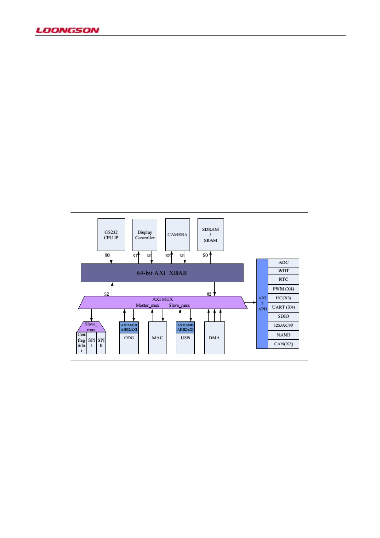
1.1 System Architecture Chart
Hierarchical bus architecture is adopted inside Loongson 1C. Processor core, memory controller, graphic display
controller, CAMERA interface module and AXI_MUX are interconnected by crossbar OTG, MAC, USB and
DMA controllers and SPI are connected to crossbar via AXI_MUX. Low-speed peripherals (I2C, I2S, PWM,
UART, etc.) are connected to crossbar via AXI2APB.
Figure 1-1 Architecture chart of Loongson 1C
1.2 Main Functions of the Chip
1.2.1 Processor core
z
Instruction sets of single core LS232 and MIPS32 are compatible, and the dominant frequency is 300MHZ.
z
It supports the highly effective dual-issue technology (one clock tick performs two instructions)
z
It supports the out-of-order issue and execution technologies such as register renaming, dynamic scheduling, and
branch prediction
z
5-stage pipeline(instruction fetch, coding, issue, execution, write back and submit ) microarchitecture
z
16KB data cache and 16KB instruction cache
z
It integrates 64bit floating point processing unit, supports the fully pipelining of 64bit floating point additive and
multiplying operation. Its hardware has accomplished the floating point division operation.
-10-
1.2.2 SDRAM Controller
z
SDRAM operation, operating frequency of 45~133MHz
z
It supports the bus width of 8/16bit parallel data.
z
It supports the auto-refresh and self-refresh functions, and page mode.
1.2.3 SRAM/NOR FLASH Controller
z
SRAM and NOR Flash direct link interface, working frequency of 66~133MHz
z
It supports the chip select pin of static memory, and can be configured separately.
z
It supports the bus width of 8bit/16bit parallel data.
1.2.4 NAND Controller
z
It supports the single capacity of 4GB NAND FLASH at most
z
It supports the FLASH of 512 bytes, 2K byte page, 4K byte page and 8K byte page.
z
Hardware ECC generation, detection and indication (software error correction)
z
It supports the data reading speed of 8~10MB/S and writing speed of 5MB/s from Flash
z
It supports the boot from NAND Flash
z
Support mode of little endian
1.2.5 Clock generator
z
It has one standard PLL input interface, and supports the external crystal as chip clock input.
z
It supports the on-chip output and can configure one way of clock for off-chip peripherals.
z
PLL configurable frequency software
1.2.6 I2S controller
z
It supports I2S input in master mode
z
It supports I2S output in master mode
z
It supports the width of 8, 16, 18, 20, 24 and 32 bits.
z
It supports audio data of mono and stereo
z
It supports the sampling frequency of (16, 22.05, 32, 44.1 and 48) kHz
z
It supports DMA transmission mode
1.2.7 AC97 controller
z
Variable sampling rate AC97 coder and decoder interfaces (48KHz and below)
z
It supports the stereo PCM and single-track MIC input
z
It supports 2-channel stereo PCM output
z
It support DMA and interrupt operation
z
It supports 16, 18 and 20bits sampling precision, and variable sampling rate.
z
It supports 16bits, and 16 entry FIFOs for each channel.
1.2.8 LCD controller
z
It support 16/24-bit pixel mode
z
It supports the display output of RGB444/555/565/888
z
It supports the pixel of 1024x768, 800x600, 640 x480 and 320 x240
z
It supports DMA transmission mode
1.2.9 Camera interface
z
It supports ITU-R BT.601/656 8bit input.
z
It supports RAW RGB, RGB565 and YUV4:2:2 data input.
z
It supports YUV, RGB888, RGB0888 and RGB565 outputs
-11-
z
It supports the pixel zooming of 320x240 and 640x480
z
It supports the pixel input of 2Kx2K at most, and the pixel can be configured.
z
It supports DMA transmission mode
1.2.10 MAC controller
z
It supports 10/100Mbps PHY device, including 10 Base-T, 100 Base-TX, 100Base-FX and 100 Base-T4;
z
It’s completely compatible with IEEE standard 802.3
z
It’s completely compatible with 802.3x full duplex flow control and half-duplex back pressure flow control
z
It supports VLAN frames
z
It supports DMA transmission mode
z
It supports standard media independent interface (MII)
z
It supports the standard simplified MII interface (RMII), and may connect the external PHY chip.
1.2.11 USB2.0 controller
z
One USB OTG2.0 controller
z
One USB HOST2.0 controller
z
It supports high-speed and full-speed mode
z
It supports DMA transmission mode
z
It’s compatible with USB Rev 1.1 and USB Rev 2.0 protocols
1.2.12 SPI controller
z
It supports two-way independent SPI interface, and each way of SPI interface supports four chip selects.
z
Follow specifications of serial peripheral interface (SPI)
z
It supports synchronous, serial and full duplex communication
z
It supports SPI master mode
z
8-bit in per transmission
z
It supports inquiries and interrupt transmission mode
z
It supports the SPI nor flash boot.
z
It supports SPI interface two-way input and output, and the maximum data transmission speed is 24~96
Mbps.
z
It supports the minimum communication rate as low as 25KB, and facilitates the matching of special device.
1.2.13 I2C controller
z
Three-channel standard I2C bus interface
z
It supports configuration of master, slave or master / slave mode
z
Programmable bus clock frequency
1.2.14 UART controller
z
It supports two full-function serial ports. Therein, the full-function serial port 0 can multiplex four two-wire serial
interfaces or two four-wire serial interfaces, and supports the smart card protocol.
z
RxD0, TxD0, RxD1, TxD1, RxD2 and TxD2 based on interrupt operation;
z
UART channel 0, 1 and 2 with IrDA 1.0
z
UART channel 0 and 1 with RTS0, CTS0, RTS1 and CTS1
1.2.15 GPIO
z
It supports 105 GPIO at most
z
All GPIO (except boot and system configuration) is defaulted as input after reset
z
All GPIO support interrupt function
z
Each GPIO pin supports the level-triggered and edge-triggered modes, and can be configured independently.
z
GPIO base pin rate up to 4MHz
-12-
1.2.16 PWM controller
z
Four-way 32bits can configure PWM timer.
z
It supports timer function
z
It supports counter function
1.2.17 RTC
z
Timing is accurate to 0.1 second
z
It supports the external crystal as RTC clock input.
z
It supports the operation powered by external battery, and later by battery after powered off.
z
The special power pin may be connected to the battery or 3.3V main power supply.
z
Provide seconds, minutes, hours, days, months and years
1.2.18 CAN controller
2-channel independent CAN controller
z
It’s compatible with CAN2.0A and CAN2.0B protocols (the passive expansion frame in PCA82C200 compatible
mode)
z
It supports CAN protocol extensions
z
Bit rate up to 1Mbits / s
1.2.19 SDIO controller
z
channel independent CAN controller
z
It’s compatible with SD Memory 2.0/MMC/SDIO 2.0 protocol.
z
It supports SDIO start
1.2.20 ADC controller
z
Sampling rate up to 1MHz at most
z
4-channel ADC input
z
It supports 4-wire and 5-wire touch screens
z
It supports continuous sampling and single sampling
z
It supports analog watchdog
-13-
2 Definition of Pin
2.1 Conventions
The instructions of Loongson 1C pin in this chapter use the following protocols:
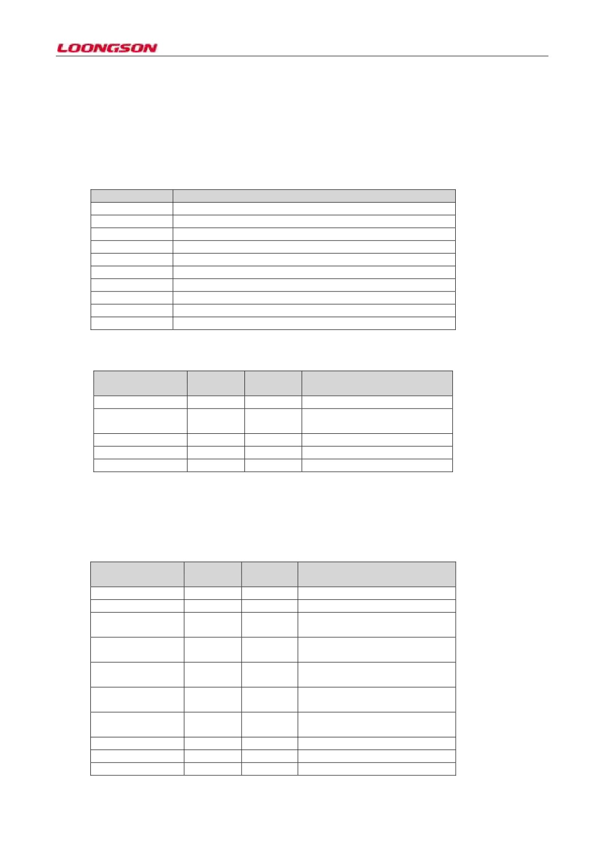
The input and output types of signals are represented by code. See Table 2-1.
Table 2-1 Signal Type Code
Code
Description
A
Simulation
DIFF I/O
Two-way difference
DIFF IN
Difference input
DIFF OUT
Difference output
I
Input.
I/O
Bidirectional
0
Output
OD
Open-drain output
P
Power supply
G
Ground
2.2 LCD Interface
Signal name
Type
Pull-up/pull-
Description
down
LCD_CLK
O
PU
LCD clock signal
LCD_HSYNC
O
PU
LCD horizontal synchronizing
signal
LCD_VSYNC
O
PU
LCD vertical synchronizing signal
LCD_EN
O
PU
LCD enable signal
LCD_DAT[15:0]
O
PU
LCD data signal
[Notes] In QFP100 package, LCD interface can’t be used. In QFP176 encapsulation, LCD may use 16bit and
24bit mode. In 16bit mode, the pin won’t be multiplexed; in 24bit mode, the low bit needs to multiplex
CAM_DAT [7:0] or MAC signal.
2.3 SDRAM Interface
Signal name
Type
Pull-up/
Description
pull-down
SD_CLK
O
-
SDRAM clock signal
SD_CKE
O
-
SDRAM clock enable signal
SD_CSn
O
-
SDRAM chip selection signal,
active low
SD_RASn
O
-
SDRAM line gating signal, effective
low level
SD_CASn
O
-
SDRAM column selection signal,
active low
SD_WE
O
-
SDRAM read-write signal, writing
as low level
SD_BA[1:0]
O
Bank signal of SDRAM, four banks
-
in total
SD_ADDR[12:0]
O
-
SDRAM address signal
SD_DATA[15:0]
I/O
-
SDRAM data signal
SD_DQM[1:0]
O
SDRAM data mask signal
-14-
2.4 SRAM/NOR Flash Interface
Signal name
Type
Pull-up/
Description
pull-down
SRAM_CSn
O
-
SRAM chip selection signal,
active low
SRAM_WEn
O
-
SRAM writing enable signal,
active low
SRAM_OEn
O
-
SRAM reading enable signal,
active low
SRAM_OEn
O
-
SRAM reading enable signal,
active low
SRAM_DATA[15:0]
I/O
-
SRAM data signal
SRAM_BHE
O
SRAM high Byte Data desired
signal
SRAM_BLE
O
SRAM low Byte Data effective
signal
2.5 I2S Interface
Signal name
Type
Pull-up/
Description
pull-down
I2S_MCLK
O
PU
I2S clock signal
I2S_BCLK
O
PU
I2S bit clock signal
I2S_LRCK
O
PU
I2S channel selection signal
I2S_DI
I
PU
I2S data serial input signal
I2S_DO
O
PU
I2S data serial output signal
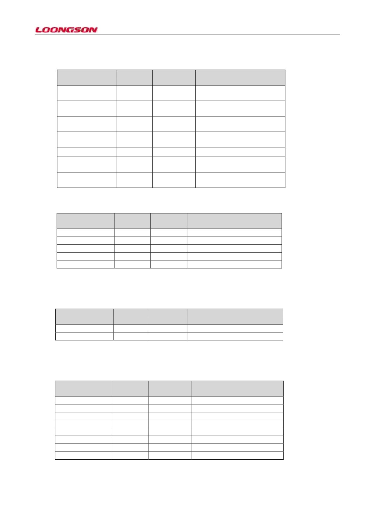
[Notes] In QFP100 package, I2S interface isn’t introduced, and needs to be multiplexed with MAC pin. In
QFP176 package, I2S interface is introduced, and can be directly used.
2.6 I 2C Interface
Signal name
Type
Pull-up/
Description
pull-down
I2C[2:0]_SCL
O
No elicitation
I2C serial clock
I2C[2:0]_SDA
I/O
No elicitation
I2C serial data
[Notes] In QFP100 and QFP176 packages, I2C interface isn’t introduced, and needs to be multiplexed with MAC,
EJTAG, LCD or CAM pin.
2.7 UART Interface
Signal name
Type
Pull-up/
Description
pull-down
UART0_TX
O
PU
UART0 data transmission
UART0_RX
I
PU
UART0 data reception
UART0_RTS
I
PU
UART0 reception request
UART0_CTS
I
PU
UART0 reception permission
UART0_DSR
I
PU
UART0 device ready
UART0_DTR
O
PU
UART0 data terminal ready
UART0_DCD
I
PU
UART0 carrier detection
UART0_RI
I
PU
UART0 ringing tips
[Notes] In QFP100 package, there is no full-function serial interface, and only two-wire type. In QFP176D
-15-
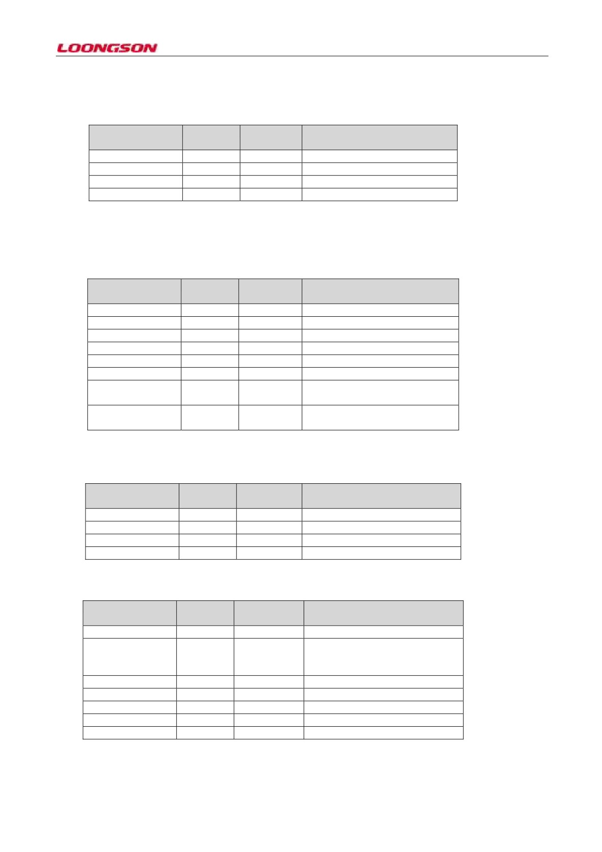
package, the full-function serial interface can be directly used.
2.8 PWM Interface
Signal name
Type
Pull-up/
Description
pull-down
PWM0
O
PU
PWMO impulse output
PWM1
O
PU
PWM1 impulse output
PWM2
O
No elicitation
PWM2 impulse output
PWM3
O
No elicitation
PWM3 impulse output
[Notes] In QFP100 package, PWM isn’t introduced and needs to be multiplexed with others. In QFP176 package,
PWM0 and PWM1 can be directly used, and PWM2 and PWM3 need to be multiplexed with others.
2.9 ADC Interface
Signal name
Type
Pull-up/
Description
pull-down
ADC_REXT
I
-
ADC reference resistor
ADC_VREF
I
-
ADC reference voltage
ADC_VDDA
I
-
ADC analog power supply
ADC_VSSA
I
-
ADC analog ground
ADC_D0
I
-
ADC Channel Zero sampling input
ADC_D1
I
-
ADC Channel 1 sampling input
ADC_XP
I
-
The 2nd channel sampling input of
touch screen X+/ADC
ADC_YP
I
-
The 3rd channel sampling input of
touch screen X+/ADC
[Notes] The AD interface can only be used In QFP176A package.
2.10 SPI Interface
Signal name
Type
Pull-up/
Description
pull-down
SPI_SCK
O
PU
SPI clock output
SPI[3:0]_CSn
O
PU
SPI chip selection 0 to 3
SPI_MOSI
O
PD
SPI data output
SPI_MISO
I
PD
SPI data input
2.11 EJTAG Interface
Signal name
Type
Pull-up/
Description
pull-down
EJTAG_SEL
I
PU
JTAG selection(0: JTAG, 1: EJTAG)
JTAG pin function multiplex (when
JTAG_SEL
I
PU
the bit is 1, select the multiplex
function)
EJTAG_TCK
I
PU
JTAG clock
EJTAG_TDI
I
PU
JTAG data input
EJTAG_TMS
I
PU
JTAG mode
EJTAG_TRST
I
PU
JTAG reset, to be pull down
EJTAG_TDO
O
PU
JTAG data output
[Notes] EJTAG_SEL select whether is JTAG or EJTAG. JTAG_SEL is used to choose JTAG multiplex function.
Please don’t be confused.
-16-
2.12 CAMERA Interface
Signal name
Type
Pull-up/
Description
pull-down
CAM_CLKOUT
O
PU
Camera reference clock output
CAM_PCLK_I
I
PU
Camera pixel clock input
CAM_HSYNC
I
PU
Camera horizontal synchronization
signal
CAM_VSYNC
I
PU
Camera vertical synchronizing signal
CAMDATA[7:0]
I
PU
Camera data input
[Notes] In QFP100 packaging, CAM isn’t bounded out and needs to be multiplexed with NAND and MAC. In
QFP176 package, CAM can be directly used.
2.13NAND Interface
Signal name
Type
Pull-up/
Description
pull-down
NAND_CLE
O
PD
NAND command latch
NAND_ALE
O
PD
NAND address latch
NAND_RD
O
PD
NAND read signal
NAND_WR
O
PD
NAND write signal
NAND_CE
O
PD
NAND chip selection 0
NAND_RDY
I
PD
NAND ready 0
NAND_D [7:0]
I/O
PD
NAND address / data lines
2.14 MAC Interface
Signal name
Type
Pull-up/
Description
pull-down
MAC_TXCK
O
PU
MII clock transmission
MAC_TXEN
O
PU
MII control transmission
MAC_TXD[3:0]
O
PU
MII data transmission
MAC_RXCK
I
PU
MII clock reception
MAC_RXDV
I
PU
MII control reception
MAC_RXD[3:0]
I
PU
MII data reception
MAC_MDCK
O
PU
SMA interface clock
MAC_MDIO
I/O
PU
SMA interface data
MAC_COL
I
PU
MAC Collision detection
MAC_CRS
I
PU
MAC carrier wave detection
[Notes] In QFP package, MAC can only use RMII mode. In QFP176 package, MII and RMII modes can be used.
2.15 OTG Interface
Signal name
Type
Pull-up/
Description
pull-down
OTG_DVDD
OTG digital power
OTG_DVSS
OTG digital ground
OTG_VDD33
OTG analog power supply
OTG_VSS33
OTG analog ground
OTG_REXT
OTG reference resistor
OTG_DP
DIFF I/O
-
OTG differential signal line D +
OTG_DM
DIFF I/O
-
OTG differential signal line D -
OTG_VBUS
OTG_VBUS
OTG_ID
OTG_ID
-17-
///////////////////////////////////////