Loongson 2F: High performance 64-bit superscalar MIPS microprocessor (2008)
Loongson 2F:
High performance 64-bit superscalar MIPS® microprocessor
Preliminary Data
Features
■
64-bit superscalar architecture
■
900 MHz clock frequency
■ Single/double precision floating-point units
■ New streaming multimedia instruction set
support (SIMD)
■
64 Kbyte instruction cache, 64 Kbyte data
HFCBGA452 (27x27x2.9mm)
cache, on-chip 512 Kbyte unified L2 cache
■ On chip DDR2-667 and PCI-X controller
The memory hierarchy is composed by the first
■
4 W @ 900 MHz power consumption:
level of 64 Kbyte 4-way set associative caches for
- Best in class for power management
instructions and data, the second level of
- Voltage/frequency scaling
512 Kbyte unified 4-way set associative cache
- Stand-by mode support
and the memory management unit (MMU) with
translation lookaside buffer (TLB).
- L2 cache disable/enable option
■ Leading edge 90 nm process technology
The Loongson microprocessor family is the
outcome of a successful collaboration started in
■
27x27 heat spreader flip-chip BGA package
2004 between STMicroelectronics and the
■ MIPS based instruction set (MIPS III
Institute of Computing Technology, part of the
compatible)
Chinese Academy of Science. Loongson
microprocessors were co-developed by
Description
STMicroelectronics and the Institute of
Computing Technology to address all the
The STLS2F01 is a MIPS based 64-bit
applications requiring high level of performance
superscalar microprocessor, able to issue four
and low power dissipation.
instructions per clock cycle among six functional
Compared to the STLS2E02 processor, the
units: two integer, two single/double-precision
STLS2F01 has an enhanced architecture
floating-point, one 64bit SIMD and one load/store
providing higher performance, reduced power
unit.
consumption, integrated DDR2 memory controller
The micro architecture is organized with nine-
and PCI-X bus interface.
stage of pipeline and support of dynamic branch
prediction.
Table 1.
Device summary
Part numbers
Package
Packing
HFCBGA452 (27x27x2.9mm)
Tray
May 2008
Rev 1
1/48
This is preliminary information on a new product now in development or undergoing evaluation. Details are subject to
1
change without notice.
Contents
Contents
1
Introduction
6
2
8
2.1
Interface signal block diagram
8
2.2
PCI bus interface signal components
9
2.3
DDR2 SDRAM interface signal components
10
2.4
Local bus signals
11
2.5
Initialization signals
12
2.6
Interrupt signals
13
2.7
JTAG signals
13
2.8
Test and control signals
13
2.9
Clock signals
14
2.10
Supply and ground
16
3
I/O bus interface description
17
3.1
PCI interface characteristic
17
3.2
Host and agent mode
17
3.3
PCI bus arbitrator
17
3.4
System interface connection
17
3.5
Local bus description
18
3.6
Interrupt handling
20
4
DDR2 SDRAM controller interface description
21
4.1
DDR2 SDRAM controller features
21
4.2
DDR2 SDRAM read protocol
21
4.3
DDR2 SDRAM write protocol
22
4.4
DDR2 SDRAM parameter format
23
4.5
DDR2 SDRAM sample mode configuration
34
5
Initialization process
35
6
Electrical characteristics
37
2/48
Contents
6.1
Absolute maximum rating
37
6.2
Recommended operation environment
37
6.3
DC parameters
38
6.4
AC parameters
39
7
Thermal characteristics
41
7.1
Thermal resistivity
41
7.2
Reflow temperature to time curve
41
8
Pin arrangement and package information
43
8.1
Pin arrangement
43
9
Package information
46
10
Revision history
47
3/48
List of tables
List of tables
Table 1.
Device summary
1
Table 2.
PCI bus signals
9
Table 3.
DDR2 SDRAM controller interface signals
10
Table 4.
Local bus signals
11
Table 5.
Initialization interface signals
12
Table 6.
Interrupt interface signals
13
Table 7.
JTAG interface signals
13
Table 8.
Clock signals
14
Table 9.
Processor internal/external frequency configuration
14
Table 10.
DDR internal/external frequency division factor
15
Table 11.
Supply and GND signals
16
Table 12.
DDR SDRAM configuration parameter register format
23
Table 13.
Absolute maximum rating
37
Table 14.
Recommended operating temperature, voltage supply and frequency
37
Table 15.
DC parameters
38
Table 16.
DC parameters (JTAG)
38
Table 17.
Clock parameters
39
Table 18.
Input setup and hold time
39
Table 19.
Input setup and hold time
40
Table 20.
Output delay time
40
Table 21.
JTAG parameters
40
Table 22.
Reflow temperature parameters
42
Table 23.
Document revision history
47
4/48
List of figures
List of figures
Figure 1.
Block diagram
6
Figure 2.
Interface signal block diagram
8
Figure 3.
STLS2F01 uniprocessor system connection
18
Figure 4.
STLS2F01 multiprocessor system connections
18
Figure 5.
Local bus read timing
19
Figure 6.
Local bus write timing
20
Figure 7.
DDR2 SDRAM read protocol
22
Figure 8.
DDR2 SDRAM write protocol
22
Figure 9.
Initialization process when in main bridge mode
36
Figure 10.
Reflow temperature to time curve
41
Figure 11.
Pin arrangement (left-hand side)
43
Figure 12.
Pin arrangement (middle)
44
Figure 13.
Pin arrangement (right-hand side)
45
Figure 14.
HFCBGA452 mechanical data & package dimensions
46
5/48
Introduction
1
Introduction
STLS processors are based on the Loongson CPU architecture licensed by
STMicroelectronics from the Institute of Computing Technology (ICT), which is part of the
Chinese Academy of Science. The STLS family belongs to the 64-bit high-end processors
for applications requiring high level of performance and efficiency in terms of cost, power
consumption and area.
Loongson CPU architecture is compatible in user mode at the MIPS III level of the MIPS
64-bit architecture.
This microprocessor achieves one of the top positions in the MIPS family for the
combination of multiple features: high clock frequency, out-of-order superscalar execution
and ability to run single-instruction-multiple data (SIMD).
STLS processors implement a superscalar, out-of-order execution pipeline with dynamic
branch prediction and non-blocking cache.
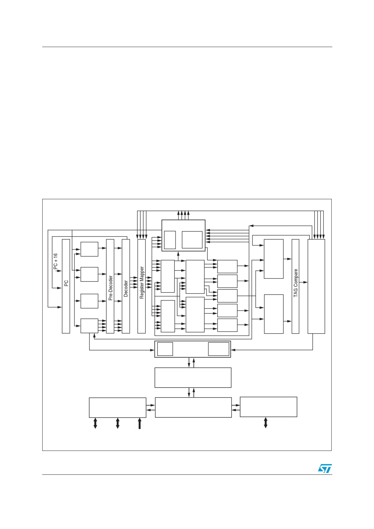
Figure 1.
Block diagram
Commit Bus
Branch Bus
Reorder Queue
Writeback Bus
BRQ
ROQ
BTB
Map Bus
D-Cache
64KB
ALU1
Fix
Integer
BHT
RS
Register
CP0
ALU2
File
Queue
AGU
ITLB
Floating
Point
FPU1
Float
TLB
Register
RS
I-Cache
File
FPU2
64KB
Refill Bus
Miss
Writeback
Cache Interface
Queue
Queue
L2 cache
DDR2 Controller
I/O Controller
AXI Crossbar
133MHz PCI-X Local IO GPIO, INT
333MHz DDR
AC00117
6/48
Introduction
The instruction pipeline allows to fetch and code four instructions per cycle and dynamically
issue the decoded instructions to five fully pipe lined function components.
The STLS2F01 uses out-of-order execution and aggressive memory hierarchy design to
maximize pipeline efficiency.
Out-of-order execution is accomplished with a combination of register renaming, dynamic
scheduling, and branch prediction techniques. The result is fewer pipeline stalls caused by
WAR (write after read) and WAW (write after write) hazards, RAW (read after write) hazards,
and control hazards. The STLS2F01 has a 64-entry physical register file for fixed- and
floating-point register renaming, a 16-entry fixed-point reservation station, and a 16-entry
floating-point reservation station that is responsible for out-of-order instruction issuing. A 64-
entry ROQ (reorder queue) ensures that out-of-order executed instructions are committed in
the program order. For precise branch prediction, a 16-entry branch target buffer (BTB), a
4K-entry branch history table (BHT), a 9-bit global history register (GHR), and a 4-entry
return address stack (RAS) are used to record branch history information.
The STLS2F01 memory hierarchy is also engineered for high performance. There is a
64 Kbyte instruction cache, a 64 Kbyte data cache, and a 512 Kbyte level-two cache. All
four-way set associative. The on-chip DDR memory allows the STLS2F01 to achieve high
memory bandwidth with low latency. The fully associative translation lookaside buffer (TLB)
has 64 entries, each mapping an odd and even page. A 24-entry memory access queue
contains a content-addressable memory for dynamic memory disambiguation and allows
the STLS2F01 to implement out-of-order memory access, non-blocking cache, load
speculation, and store forwarding.
The STLS2F01 has two fixed-point functional units, two floating-point functional units, and
one memory access unit. The floating-point units can also execute 32- or 64-bit fixed-point
instructions and 8- or 16-bit SIMD fixed-point instructions through extension of the fmt field
of the floating-point instructions. The SIMD unit extends the STLS2E02 with new XX SSE2
type instructions.
The basic pipeline stages of the STLS2F01 include instruction fetch, pre-decode, decode,
register rename, dispatch, issue, register read, execution, and commit.
The STLS2F01 device is manufactured in ST 90 nm CMOS technology.
The STLS2F01 is an evolution of the STLS2E02 with enhanced I/O and memory accessing
bandwidth and a software working frequency changing scheme.
The STLS2F01 has a standard 32-bit PCI/PCI-X interface, a standard 64-bit DDR2
interface, an 8/16-bit local I/O interface, a 4-bit GPIO interface.
The STLS2F01 achieves a higher memory access bandwidth by utilizing a 64-bit DDR2
memory controller.
Compared to its predecessor, the STLS2F01 provides better power management ability by
using a software manageable working frequency changing scheme. The operating system
can utilize this feature to change the processor frequency according to the workload.
The STLS2F01 integrates a video accelerate module in its write data path to the PCI/PCI-X
controller. Coupled with software drivers, the video accelerate module can transfer YUV
format video data to RGB format and zoom automatically. This greatly reduces the
processor's workload when the system utilizes a simple VGA controller.
The cores are centered on 2x2 AXI cross bar with 128-bit width data bus. The CPU core and
PCI/PCI-X slave takes up two master ports, DDR2 controller one slave port, and all other
modules including the PCI/PCI-X master share one slave port.
7/48
2
2.1
Interface signal block diagram
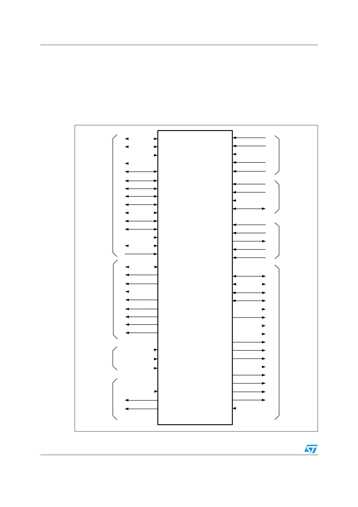
The STLS2F01’s interface signals are showed in Figure 2.
Note: The arrow indicates signal directions, e.g. input, output or bidirectional.
Figure 2.
Interface signal block diagram
PCI AD[31:0]
SYSCLK
PCI CBEn[3:0]
MEMCLK
C
P
CLKSEL [9:0]
L
PCI REQ [6:1]
O
C
TESTCLK
C
I
PCI GNT [6:1]
K
PCI REQ [0]
PCI CLK
I
N
T
PCI GNT [0]
I
NMIn
E
N
PCI PAR
R
T
INTn [3:0]
F
E
PCI PERR
A
PCI IRQn [3:0]
R
C
PCI SERR
R
E
GPIO [3:0]
U
PCI FRAMEn
P
T
S
PCI IRDYn
I
TCK
G
PCI TRDYn
N
TDI
A
PCI DEV SELn
J
L
TDO
T
S
PCI STOPn
A
TMS
G
PCI ID SEL
TRST
L
LIO AD [15:0]
O
C
LIO A [7:0]
DDR2 DQ[63:0]
A
Loongson2F
L
LIO C Sn
DDR2 CB[7:0]
D
D
B
LIO ROMC Sn
DDR2 DQ Sp[8:0]
R
U
2
LIO WRn
DDR2 DQ Sn[8:0]
S
S
LIO RDn
DDR2 A[14:0]
D
S
R
I
LIO ADLOCK
DDR2 DQM[8:0]
A
G
N
M
LIO DIR
DDR2 CKp[5:0]
A
I
L
LIO DEN
DDR2 CKn[5:0]
N
S
T
DDR2 CKE[3:0]
E
R
SYSRESETn
DDR2 ODT[3:0]
I
F
N
DDR2 SC Sn[3:0]
A
PCI RESETn
I
C
T
DDR2 BA[2:0]
E
PCI CONFIG [7:0]
DDR2 RASn
S
T
I
E
DDR2 CASn
G
S
N
T
TEST CTRL [7:0]
DDR2 WEn
A
&
L
C
PLLCLOCK0
DDR2 GATEO[3:0]
S
O
N
PLLCLOCK1
DDR2 GATEI[3:0]
T
R
O
L
8/48
2.2
PCI bus interface signal components
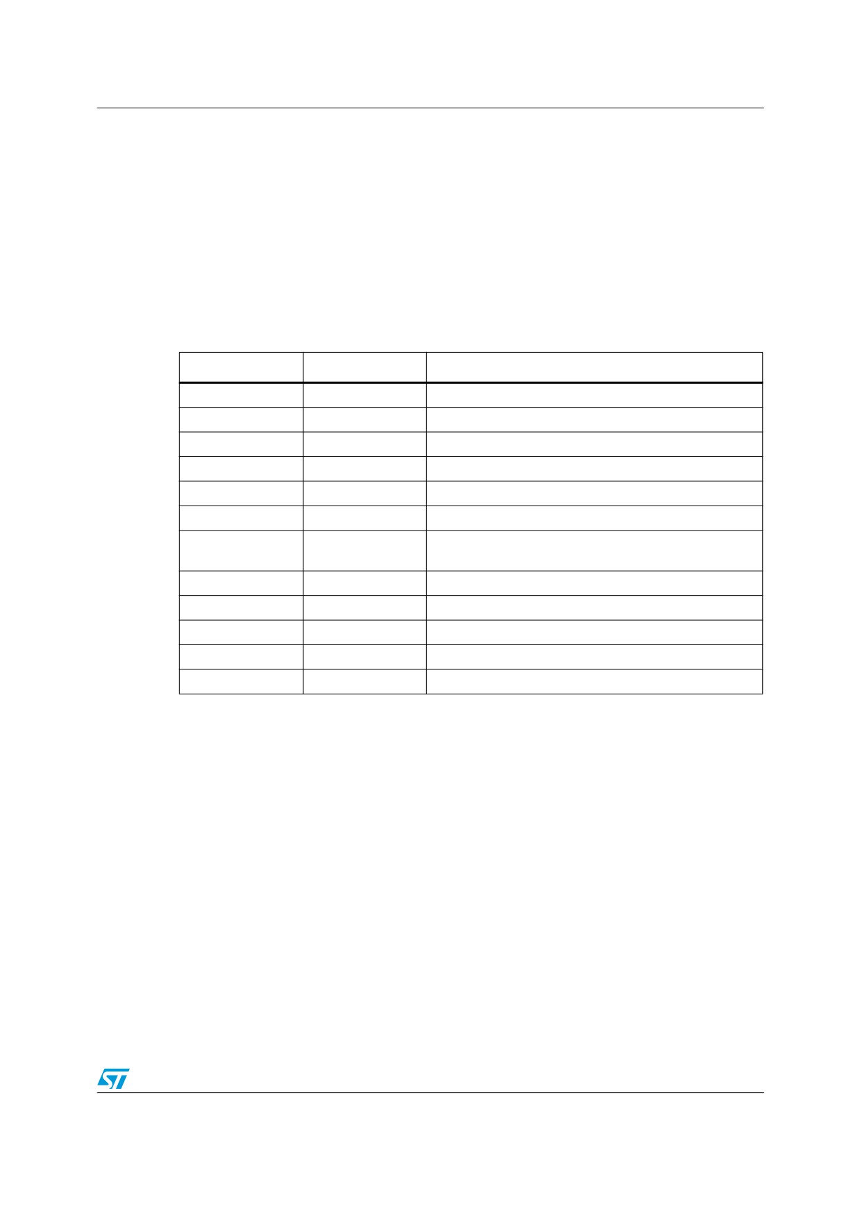
The STLS2F01’s PCI bus signal includes:
●
32-bit address data bus
●
4-bit command data ID bus
●
14-bit bus arbitrator
●
7-bit interface control
●
2-bit error report signals
The STLS2F01’s PCI bus signals are listed in Table 2.
Table 2.
PCI bus signals
Name
Input/output
Description
PCI_AD[63:0]
I/O
PCI address/data bus
PCI_CBEn[7:0]
I/O
PCI command/byte
PCI_PAR
I/O
Address/data parity check signal
PCI_REQn[6:1]
I
External Request
PCI_REQn[0]
I/O
External request input/request output to external arbiter
PCI_GNT[6:1]
O
PCI bus grant to external device
PCI bus grant to external device / grant input from
PCI_GNT[0]
I/O
external arbiter
PCI_FRAMEn
I/O
PCI bus cycle frame
PCI_IRDYn
I/O
PCI initiator ready
PCI_TRDYn
I/O
PCI target ready
PCI_STOPn
I/O
PCI stop
PCI_DEVSELn
I/O
PCI device select
9/48
2.3
DDR2 SDRAM interface signal components
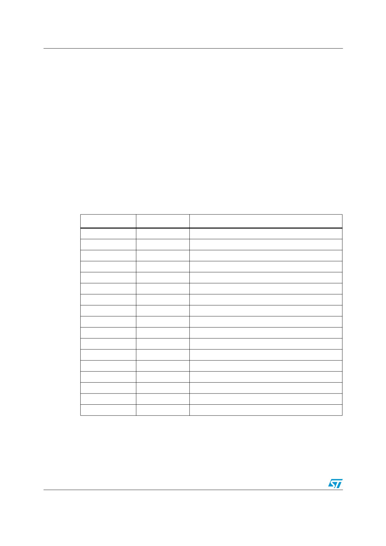
The STLS2F01 includes a built-in memory controller fully compatible with DDR2 SDRAM
industry standard (JESD79-2B). These signals include:
●
72-bit bidirectional data bus (ECC included)
●
9-bit bidirectional data strobe differential signal (ECC included)
●
9-bit data mask signal (ECC included)
●
15-bit address bus
●
7-bit bank and chip select signal
●
6-bit differential clock
●
4-bit clock enable
●
3-bit command bus
●
4-bit delay sample input/output signal
●
4-bit ODT (on die termination) signal
The STLS2F01 DDR2 SDRAM controller signals are listed in Table 3.
Table 3.
DDR2 SDRAM controller interface signals
Name
Input/output
Description
DDR2_DQ[63:0]
IO
DDR2 SDRAM data bus
DDR2_CB[7:0]
IO
DDR2 SDRAM data ECC data bus
DDR2_DQSp[8:0]
IO
DDR2 SDRAM data strobe (ECC included)
DDR2_DQSn[8:0]
IO
DDR2 SDRAM data strobe (ECC included)
DDR2_DQM[8:0]
O
DDR2 SDRAM data mask (ECC included)
DDR2_A[14:0]
O
DDR2 SDRAM address bus
DDR2_BA[2:0]
O
DDR2 SDRAM bank address signal
DDR2_WEn
O
DDR2 SDRAM write enable
DDR2_CASn
O
DDR2 SDRAM column select enable
DDR2_RASn
O
DDR2 SDRAM row select enable
DDR2_SCSn[3:0]
O
DDR2 SDRAM chip select
DDR2_CKE[3:0]
O
DDR2 SDRAM clock enable
DDR2_CKp[5:0]
O
DDR2 SDRAM phase clock output
DDR2_CKn[5:0]
O
DDR2 SDRAM phase inversion clock output
DDR2_GATEI[3:0]
I
DDR2 SDRAM delay sample input signal
DDR2_GATEO[3:0]
O
DDR2 SDRAM delay sample output signal
DDR2_ODT[3:0]
O
DDR2 SDRAM on-die termination signal
10/48
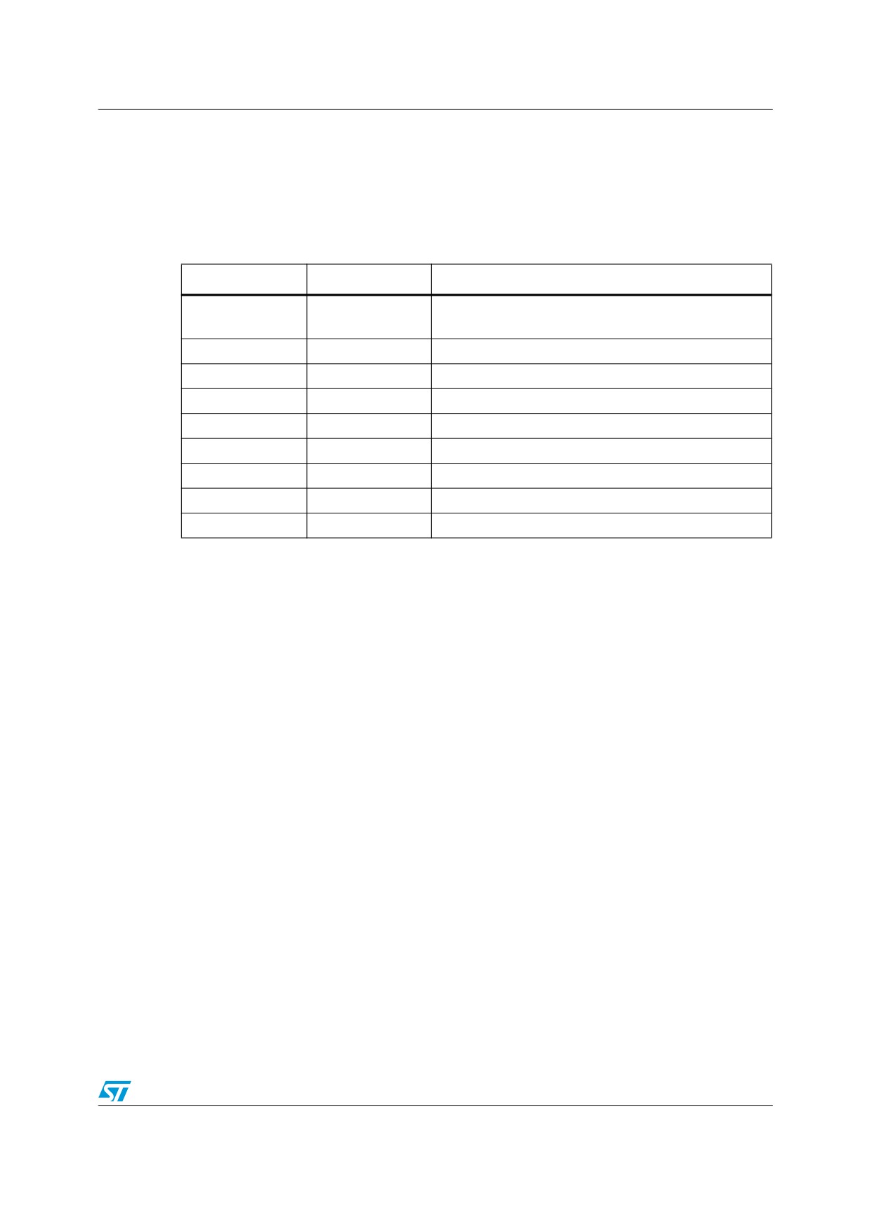
2.4
Local bus signals
The local bus provides a simple bus interface for system boot ROM and I/O device. The
interface is designed for chip-connect simplicity.
The local bus signals are listed in Table 4.
Table 4.
Local bus signals
Name
Input/output
Description
Local I/O address and data bus
LIO_AD[15:0]
I/O
When ADLOCK valid output the most significant 16 bits
LIO_A[7:0]
O
Lowest significant 8-bit address bus
LIO_CSn
O
Local I/O chip select
LIO_ROMCSn
O
Local I/O ROM chip select
LIO_WRn
O
Local I/O write enable
LIO_RDn
O
Local I/O read enable
LIO_ADLOCK
O
Local I/O address lock
LIO_DIR
O
Local I/O direction
LIO_DEN
O
Local I/O device enable
11/48
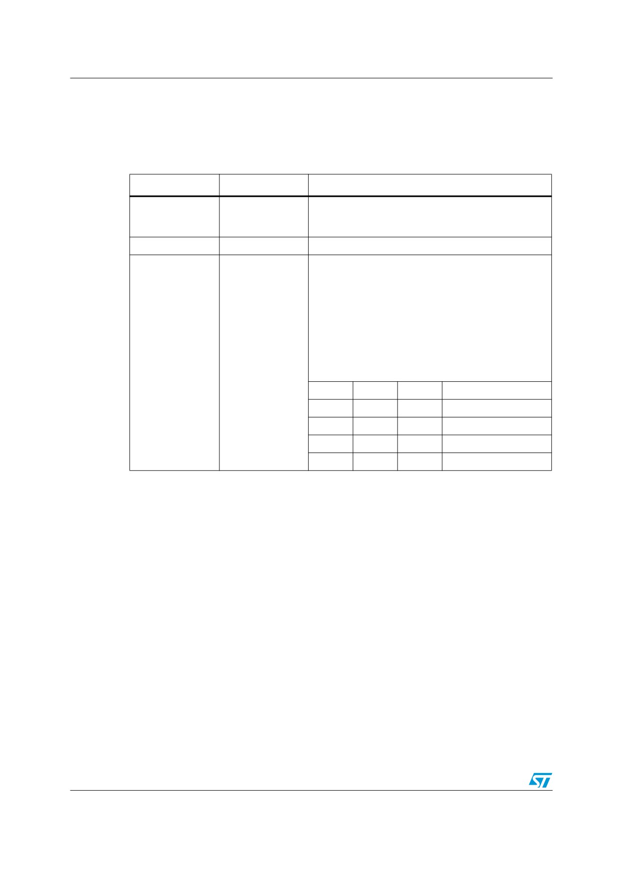
2.5
Initialization signals
Table 5 provides the names, definitions, and directions and descriptions of the initialization
signals.
Table 5.
Initialization interface signals
Name
Input/output
Description
System reset. Low state of the signal must be maintained
SYSRESETn
I
more than one SYSCLK period. It can be asynchronous
to SYSCLK.
PCI_RESETn
I/O
PCI interface reset.
PCI Configuration
7 undefined
6:5 PCI-X bus speed selection
4 PCI-X bus mode
3 Master mode
2 Start from PCI
1 External PCI arbitration
0
16-bit starting ROM
PCI_CONFIG
I
Note:
6
5
4
PCI-X BUS mode
0
0
0
PCI 33/66
0
1
1
PCI-X 66
1
0
1
PCI-X 100
1
1
1
PCI-X 133
The STLS2F01 processor includes two reset signals: SYSRESETn and PCI_RESETn.
● SYSRESETn: This reset signal is the only way to reset whole STLS2F01 processor.
SYSCLK and MEMCLK must provide stable clock when SYSRESETn is valid. The
width of SYSRESETn should be more than one clock period. Internal reset-control
begins to reset internal logic when reset signal is invalid. The internal reset will be
finished after 64K SYSCLK cycle. Then reset exception vector could be executed
● PCI_RESETn: This signal works as output when the processor works as a system
main bridge. And the reset of PCI-X devices in the system must be controlled by the
signal. When the processor works as PCI/PCI-X devices used in other system, the
signal works as input to reset the PCI interface of processor. (Note: Resetting PCI
interface when process is running may cause the processor stop working)
PCI_CONFIG: defines the mode of working of the processor interface. It must keep stable
during system reset, so that software could read this value from internal register after
system started. The PCI address of the first instruction is 0x1fc00000 when system starting
from PCI is configured. Otherwise the first instruction will be fetched from address 0 of Local
Bus ROM.
12/48
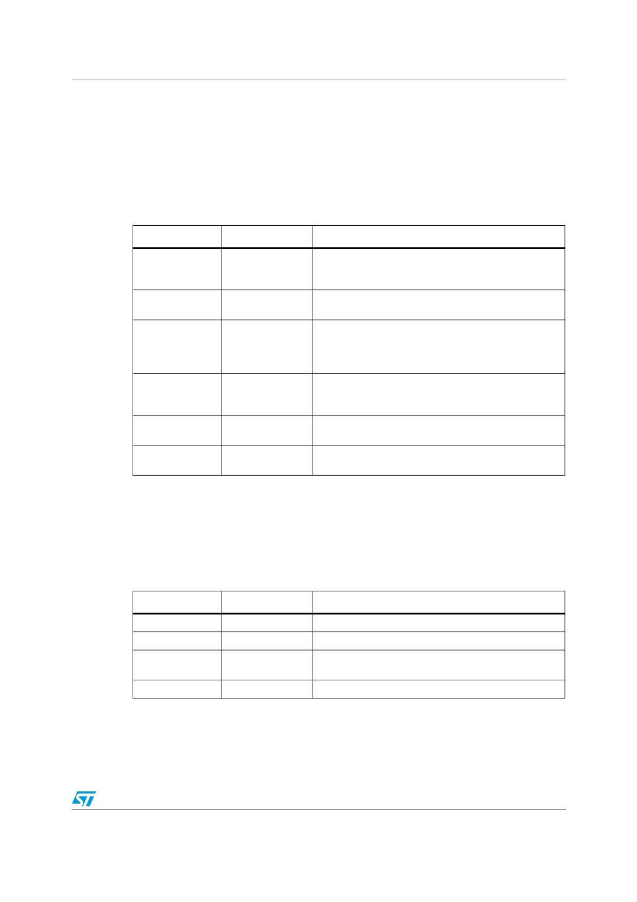
2.6
Interrupt signals
The STLS2F01 processor supports up to 12 external interrupts and one non-maskable
interrupt (NMI). There are 4 PCI interrupt signals, 4 special interrupt signals and 4
configurable GPIO interrupt. In addition, there are 3 internal interrupts, two PCI bus error
report signals and one DDR2 control interrupt. When an interrupt takes place, the processor
handles the exception. Table 6 shows the names, definitions, directions and descriptions of
the interrupt signals.
Table 6.
Interrupt interface signals
Name
Input/output
Description
4 external interrupt signals. OR operations are performed
INTn[3:0]
I
on these signals with interrupt register from bit 5 to bit 2
separately.
NMI. An OR operation is performed on the NOT-value of
NMIn
I
this signal and the interrupt register’s 6th bit.
These interrupts should be enabled in the interrupt
controller and can be configured as different active power
GPIO[3:0]
I/O
level and different trigger mode. These interrupts could be
routed to interrupt register bit 0/1.
These interrupts should be enabled in the interrupt
PCI_IRQ[3:0]
I
controller and low active. These interrupts could be routed
to interrupt register bit 0/1.
PCI bus parity error, high pulse active. These interrupts
PCI_PERR
I/O
could be routed to interrupt register bit 0/1.
PCI bus error, high pulse active. These interrupts could be
PCI_SERR
I/O
routed to interrupt register bit 0/1.
2.7
JTAG signals
The STLS2F01 provides a JTAG-compliant boundary scan interface. The JTAG interface is
particularly suitable for testing the processor pins for connectivity. The Table 7 provides the
names, definitions, directions and descriptions of the JTAG signals.
Table 7.
JTAG interface signals
Name
Input/output
Description
TDI
I
JTAG serial scan data input
TDO
O
JTAG serial scan data input
JTAG Command, indicating that the input serial data is a
TMS
I
command.
TCK
I
TAG serial scan clock
2.8
Test and control signals
On the STLS2F01 chip, the test signals are only used for chip physical test, e.g. scan chain
test. When the chip works normally, these signals are set invalid 1.
13/48
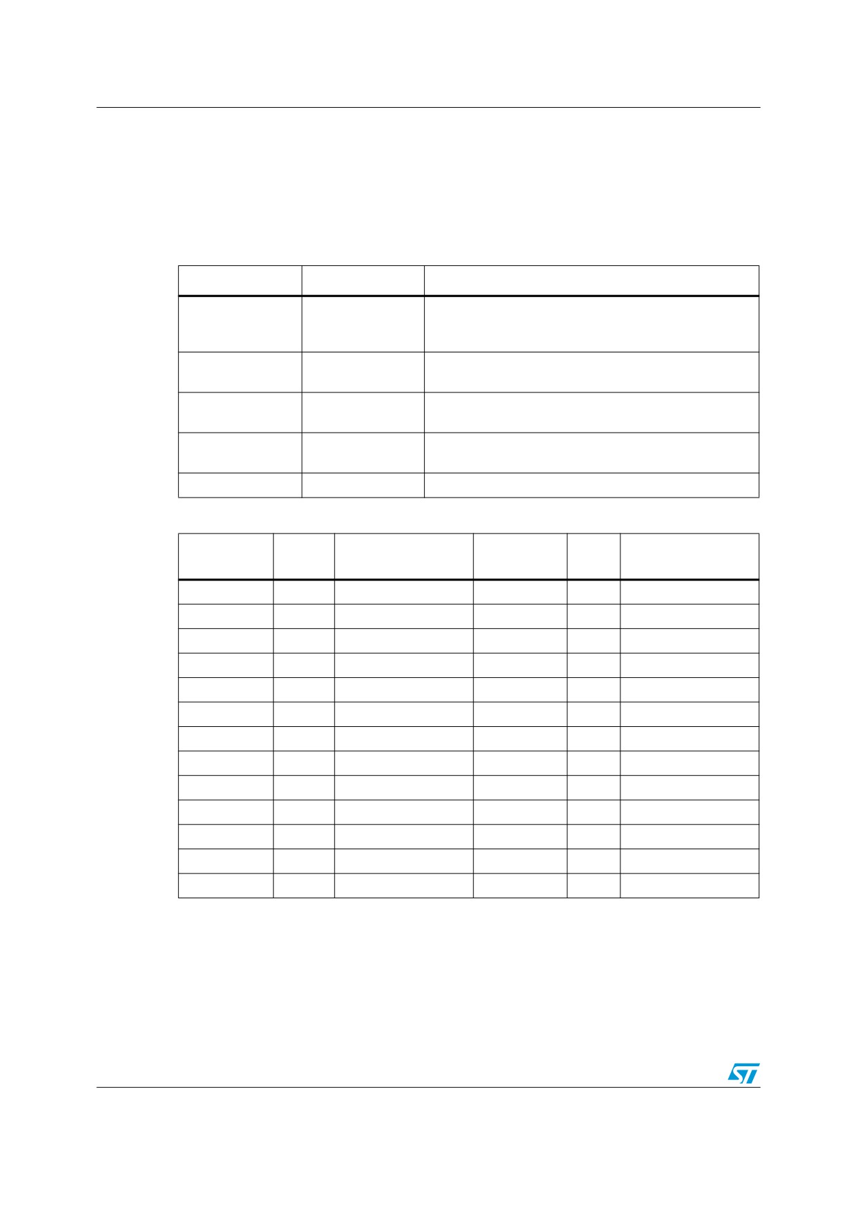
2.9
Clock signals
For information about clock on the STLS2F01 chip, see Table 8. The processor has three
system input clock signals. (SYSCLK, MEMCLK and PCI_CLK) The TESTCLK is only used
for chip test. The CPU core clock and DDR2 control clock are generated separately by PLL
using SYSCLK and MEMCLK. The frequency division is controlled by CLKSEL. For more
about the division factor, see Table 9 and Table 10.
Table 8.
Clock signals
Name
Input/output
Description
System input clock, which drives the built-in PLL to
SYSCLK
I
generate core clock. It also used as clock of system reset
circuit.
DDR2 controller input clock, which is used by the built-in
MEMCLK
I
PLL to generate DDR2 control clock.
PLL frequency division control signal of core clock, see
CLKSEL[4:0]
I
Table 9.
PLL frequency division control signal of DDR2 controller
CLKSEL[9:5]
I
clock, see Table 10.
PCI_CLK
I
Clock for PCI and Local bus interface.
Table 9.
Processor internal/external frequency configuration
Multi.
Input frequency
Multi.
Input frequency
CLKSEL[4:0]
CLKSEL[4:0]
factor
range (MHz)
factor
range (MHz)
11xxx
1
-
10000
2.25
88.9~177.8
01100
6.5
61.5~123.1
10001
2.5
80.0~160.0
01101
7
57.1~114.3
10010
2.75
72.7~145.5
01110
7.5
53.3~106.7
10011
3
66.7~133.3
01111
8
50.0~100.0
10100
3.25
61.5~123.1
00000
9
88.9~177.8
10101
3.5
57.1~114.3
00001
10
80.0~160.0
10110
3.75
53.3~106.7
00010
11
72.7~145.5
10111
4
50.0~100.0
00011
12
66.7~133.3
01000
4.5
88.9~177.8
00100
13
61.5~123.1
01001
5
80.0~160.0
00101
14
57.1~114.3
01010
5.5
72.7~145.5
00110
15
53.3~106.7
01011
6
66.7~133.3
00111
16
50.0~100.0
14/48
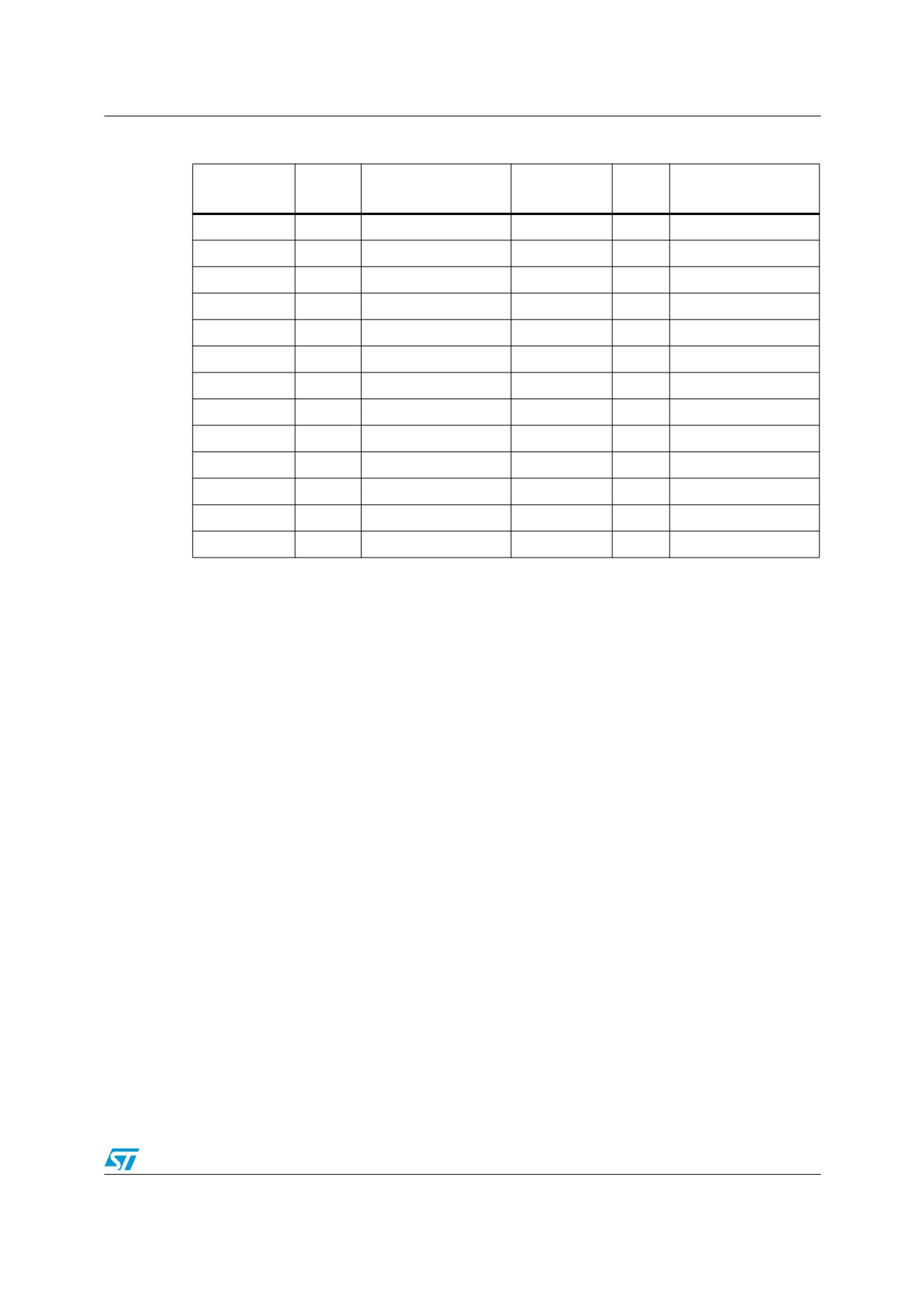
Table 10. DDR internal/external frequency division factor
Multi.
Input frequency
Multi.
Input frequency
CLKSEL[9:5]
CLKSEL[9:5]
factor
range (MHz)
factor
range (MHz)
11000
1.125
88.9~177.8
10100
3.25
61.5~123.1
11001
1.25
80.0~160.0
10101
3.5
57.1~114.3
11010
1.375
72.7~145.5
10110
3.75
53.3~106.7
11011
1.5
66.7~133.3
10111
4
50.0~100.0
11100
1.625
61.5~123.1
01000
4.5
88.9~177.8
11101
1.75
57.1~114.3
01001
5
80.0~160.0
11110
1.875
53.3~106.7
01010
5.5
72.7~145.5
11111
2
50.0~100.0
01011
6
66.7~133.3
10000
2.25
88.9~177.8
01100
6.5
61.5~123.1
10001
2.5
80.0~160.0
01101
7
57.1~114.3
10010
2.75
72.7~145.5
01110
7.5
53.3~106.7
10011
3
66.7~133.3
01111
8
50.0~100.0
00xxx
1
-
15/48
2.10
Supply and ground
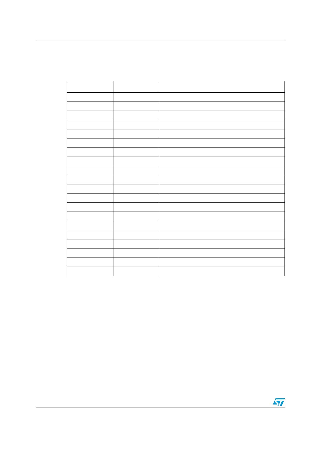
See Table 11 for supply and GND signals at the STLS2F01.
Table 11. Supply and GND signals
Name
Input/output
Description
vdd
PWR
1.2 V CPU core voltage
gnd
GND
1.2 V CPU core ground
Vdde1v8
PWR
1.8 V DDR2 power supply
gnde
GND
1.8 V DDR2 and 3.3V I/O ground
Vdde3v3
PWR
3.3 V IO power supply
DDR2_VREF
I
0.9 V DDR reference voltage input
pll_vdd_1
PWR
1.0 V PLL 1 digital power supply
pll_gnd_1
GND
1.0V PLL 1 digital ground
pll_vdd_0
PWR
1.0V PLL 0 digital power supply
pll_gnd_0
GND
1.0V PLL 0 digital ground
Pllio_vdde1v8
PWR
1.8V PLL I/O power supply
pllio_gnde
GND
1.8V PLL I/O ground
pllio_vdd
PWR
1.2V PLL I/O power Supply
pllio_gnd
GND
1.2V PLL I/O ground
Pll_vdde1v8_1
PWR
1.8V PLL 1 analog power supply
Pll_gnde_1
GND
1.8V PLL 1 analog ground
Pll_vdde1v8_0
PWR
1.8V PLL 0 analog power supply
Pll_gnde_0
GND
1.8V PLL 0 analog ground
comp1v8_gnd
GND
Compensation reference current ground
comp1v8_resistor
I
Compensation external resistor input
16/48
I/O bus interface description
3
I/O bus interface description
The STLS2F01 processor I/O interface consists of PCI bus and Local bus. PCI bus is used
to for generic peripheral devices interface, while Local bus is the simple interface to boot or
debug the processor.
3.1
PCI interface characteristic
The PCI interface features:
● PCI 2.3 and PCI-X 1.0 compatible
● Support PCI 66 MHz and PCI-X133 MHz
● Support dual address cycle for 64-bit addressing
● Support 8 outstanding master request in PCI-X mode
● Support 4 delay-split read request in PCI-X mode
3.2
Host and agent mode
The STLS2F01’s PCI interface could be worked in Host mode or Agent mode. It depends on
initial signal PCI_CONFIG. When the processor works in Host mode, the interface initializes
the bus device according to the value of PCI_CONFIG[6:4]. In this case, PCI_IDSEL could
connect to GND directly. When the processor works in Agent mode, the initial value of PCI
bus defines the work-mode of the interface. In Host mode, on the system main board, the
value of PCI_CONFIG[6:4] should be set according to the ability of bus device. (Please refer
to PCI-X 1.0 standard)
3.3
PCI bus arbitrator
PCI/PCI-X bus arbitrator built in STLS2F01 supports 7 external masters at most. The
arbitration rules are two levels Round Robin scheduling. The level of each request is
determined by software configuration. The bus is granted to insert a dummy cycle during
switching. Bus parking can be configured as the last master or any specified master.
The internal request/grant wire of interface could be set to connect to the number 0
request/grant wire by PCI_CONFIG [1], so that the external bus arbitrator can be used.
3.4
System interface connection
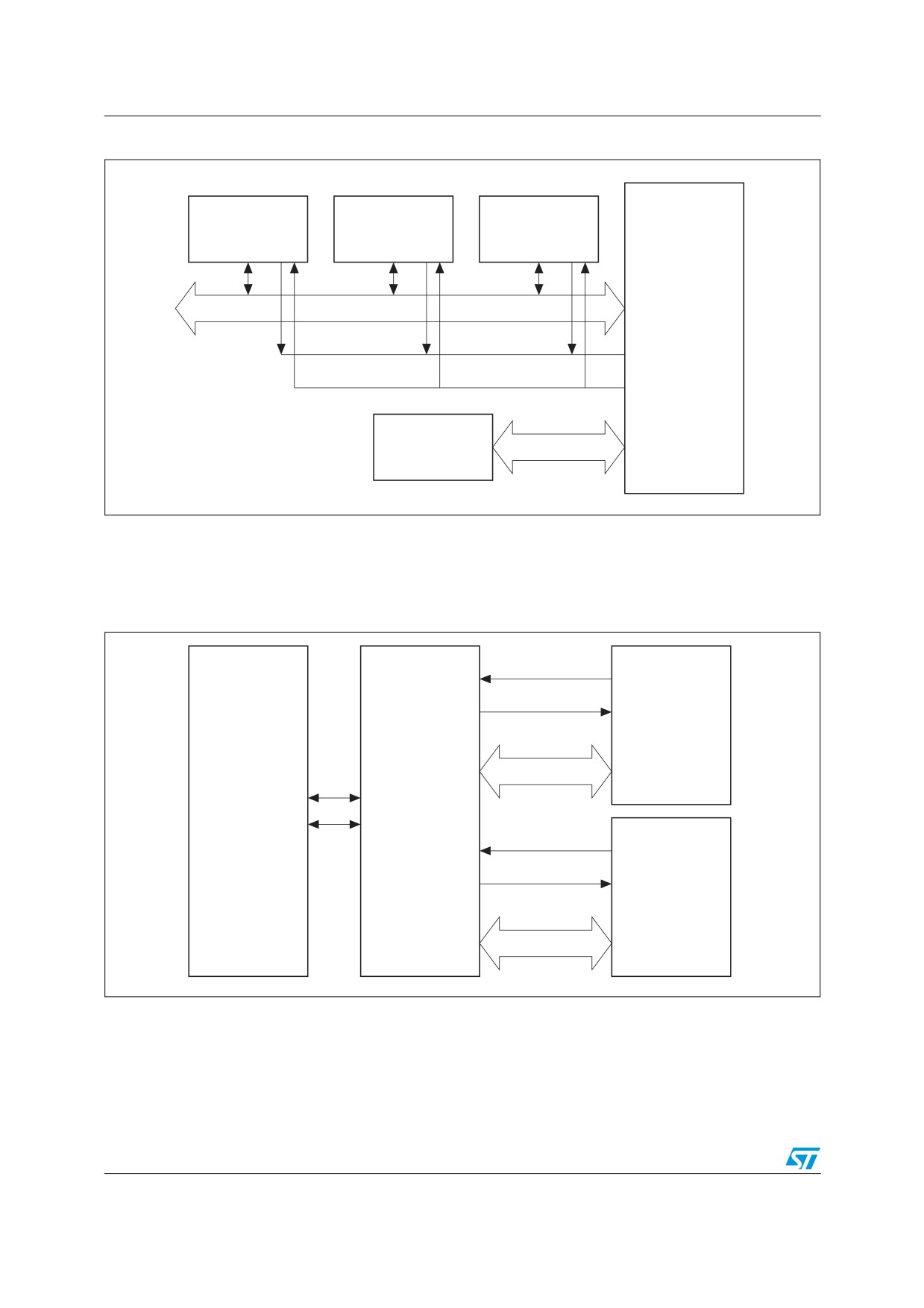
The STLS2F01 processor can be easily implemented in uniprocessor system. Since no
multi-processor cache coherence protocol is supported in PCI interface, the cache
coherence should be managed by software in multiprocessor system.
● Single processor system connection
17/48
I/O bus interface description
Figure 3. STLS2F01 uniprocessor system connection
PCI Dev
PCI Dev
PCI Dev
PCI Bus
Loongson2F
PCI_REQ
PCI_GNT
Boot Rom
Local Bus
● Multiprocessor system connections
Figure 4. STLS2F01 multiprocessor system connections
PCI_REQn
PCI_GNTn
Loongson2F
PCI Bus
I/O
Chipset
PCI_REQn
PCI_GNTn
Loongson2F
PCI Bus
3.5
Local bus description
Local bus is a simple peripheral interface. It’s mainly used to connect to boot ROM. There
are two chip select signals, and corresponding configurable data width and access delay.
18/48
I/O bus interface description
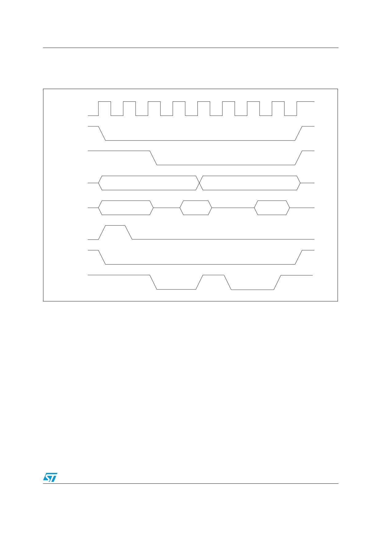
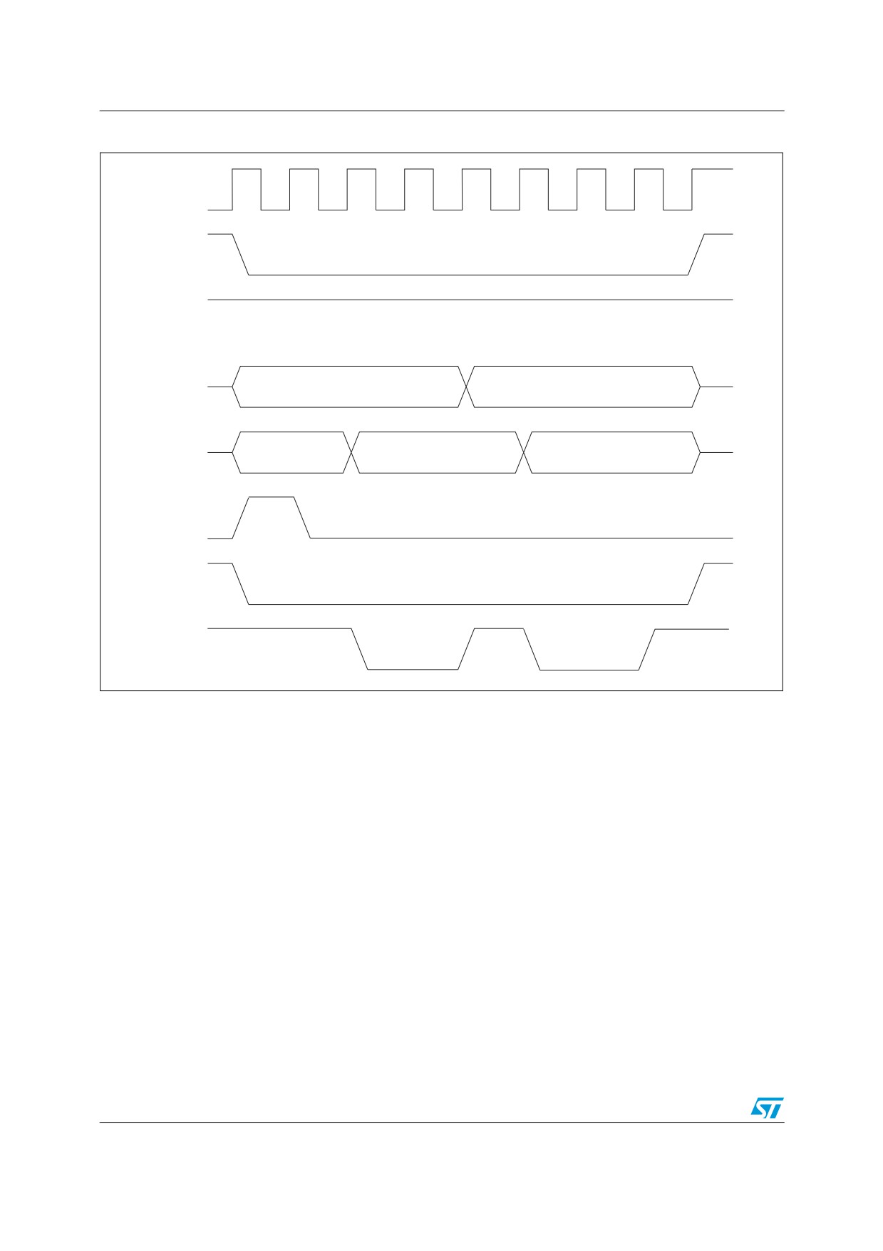
The read and write timing are shown in the Figure 5 and Figure 6. When the data width is
16-bit, the output address can be generated by shifting the physical address right one bit.
Figure 5. Local bus read timing
pciclk
lioden
liodir
lioaddr
addr[7:0]
addr[7:0]+1
lioad
addr[23..8]
data
data
lioadlock
liocs
liord
19/48
I/O bus interface description
Figure 6. Local bus write timing
pciclk
lioden
liodir
lioaddr
addr[7:0]
addr[7:0]+1
lioad
addr[23:8]
data_0
data_1
lioadlock
liocs
liowr
3.6
Interrupt handling
An interrupt controller is built in STLS2F01 processor to handle internal and external
interrupt. The most significant 4 bits of the interrupt INTn[5:0] in STLS2E01 are still being
used as interrupt in STLS2F01, while the other two bits are used for new interrupt in
STLS2F01, such as PCI_IRQ and GPIO, etc.
How to handle the interrupt between processors: the interrupt initiator writes the dedicated
interrupt register in the chipset. Upon receiving the request for interrupt transmission, the
chipset will request the target processor for interrupt. The processor handles the request in
the same way as the previous STLS2E01 and beyond.
20/48
DDR2 SDRAM controller interface description
4
DDR2 SDRAM controller interface description
The STLS2F01 integrates a built-in memory controller compliant with DDR2 SDRAM
standard (JESD79-2B). The STLS2F01 provide JESD79-2B-compliant read/write
operations onto memory.
4.1
DDR2 SDRAM controller features
The STLS2F01 CPU supports up to 4 physical memory by using two DDR SDRAM chip
select signals, with a 18-bit address bus (15-bit row/column address and 3-bit logic bank
bus). The maximum address space is 128GB (237 bytes).
This device supports all the JESD79-2B-compatible memory chips. The DDR2 controller
parameters can be set to support specific memory chip type. The maximum number of chip
selection (CS_n) is 2-bit. The maximum width of row address (RAS_n) is 15-bit, and the
maximum width of column address (CAS_n) is 14-bit. And there is 3-bit logic bank bus
(BANK_n).
For example, in the 4GB address space configuration of 2-bit CS_n, 3-bit BANK_n, 12-bit
RAS_n and 12-bit CAS_n, the physical memory address CPU required can be translated
into row/column address as shown in the DDR2 SDRAM row/column address translation
paragraph.
DDR2 SDRAM row/column address translation
36
32
31
30
29
18
17
15
14
3 2
0
CS_n
RAS_n
BANK_n
CAS_n
Byte_enable
5
2
12
3
12
3
The built-in memory controller IC receives only memory read/write requests from a
processor or external device. The controller IC is in Slave state whenever memory are read
or written.
A dynamic page management policy is implemented on the integrated memory controller.
For one access to memory, the controller selects Open Page/Close Page strategies on a
hardware circuit, without software designers’ intervention. The memory controller features:
● Full pipeline support to command and read/write data of interface
● Increasing bandwidth by merging and sorting memory command
● Modify fundamental parameters through the configuration of register read/write ports
● Built-in delay compensation circuit (DCC), it is used to send/receive data reliably
●
1-bit and 2-bit error detection, 1-bit error correction by error correcting-code (ECC)
● Frequency: 133 MHz - 333 MHz
4.2
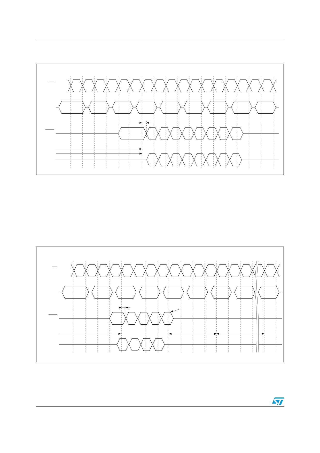
DDR2 SDRAM read protocol
As showed in Figure 7 DDR2 SDRAM read protocol, the command (CMD) includes RAS_n,
CAS_n and WE_n. When a read request happens, RAS_n=1,CAS_n=0,and WE_n=1.
21/48
DDR2 SDRAM controller interface description
Figure 7. DDR2 SDRAM read protocol
CAS latency = 3, read latency = 3, burst length = 8
T0
T1
T2
T3
T4
T5
T6
T7
T8
CK/CK
CMD
READ A
NOP
NOP
NOP
NOP
NOP
NOP
NOP
NOP
≤ tDQSCK
DQS/DQS
CL=3
RL=3
DQS
DOUTA1
DOUTA1
DOUTA2
DOUTA3
DOUTA4
DOUTA5
DOUTA6
DOUTA7
4.3
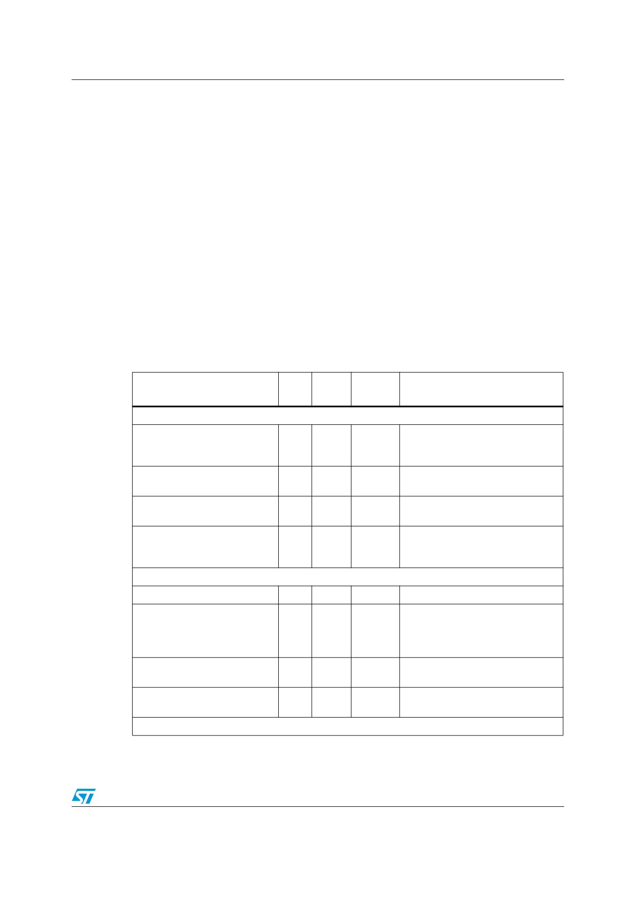
DDR2 SDRAM write protocol
As showed in Figure 8 DDR2 SDRAM write protocol, the command (CMD) includes RAS_n,
CAS_n and WE_n. When a write request happens, RAS_n=1, CAS_n=0,and WE_n=0.
Unlike a read transaction, DQM is used to identify the write mask. In other words, the
number of written bytes is needed. DQM is synchronous with DQS.
Figure 8. DDR2 SDRAM write protocol
CAS latency = 3, write latency = read latency = 2, burst length = 4
T0
T1
T2
T3
T4
T5
T6
T7
Tn
CK/CK
CMD
Bank A
WRITE A
NOP
NOP
NOP
NOP
NOP
Precharge
NOP
Activate
Completion of
≤ tDQS6
the Burst Write
DQS/DQS
WL = RL - 1 = 2
≥ WR
≥
tRP
DQS
DINA0
DINA1
DINA2
DINA3
22/48
DDR2 SDRAM controller interface description
4.4
DDR2 SDRAM parameter format
Since different DDR2 SDRAMs may be used in the system, DDR2 SDRAM needs
configuration after power-on reset. The JESD79-2B standard defines detailed configuration
operation and process. DDR2 is not available before the memory is initialized. Memory
initialization sequence:
1.
System reset, aresetn signal is set 0, all registers content will be initial value.
2.
System reset release, aresetn signal is set 1.
3.
Issue 64-bit write command to configuration register, all 29 registers are configured. If
register CTRL_03 is written in this step, the parameter of start should be set 0.
4.
Issue 64-bit write command to register CTRL_03. Set the parameter of start to 1. Then,
memory controller will send initial instruction to memory automatically.
In the STLS2F01 processor design, after the system motherboard is initialized, the DDR2
SDRAM controller needs configure memory type before the memory is used. Specifically,
corresponding configuration parameters are written into the 29 64-bit registers
corresponding to the physical address 0x0000 0000 0FFF FE00. In one register, one,
multiple or partial parameter data can be included. The configuration register and its
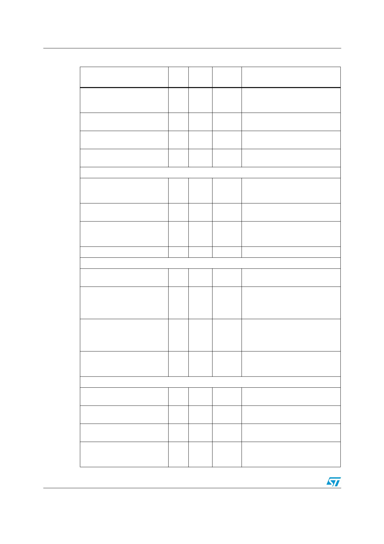
parameters are shown in Table 12 Note: the bits not used are all reserved bits.
Table 12. DDR SDRAM configuration parameter register format
Default
Parameters
Bits
Range
Description
value
CONF_CTL_00[31:0] Offset: 0x00
DDR2 667:0x00000101
Initiate auto-refresh when specified
AREFRESH
24:24
0x0
0x0-0x1
by AUTO_REFRESH_MODE. Write-
only
Enable auto pre-charge mode of
AP
16:16
0x0
0x0-0x1
controller.
Enable address collision detection
ADDR_CMP_EN
8:8
0x0
0x0-0x1
for command queue placement logic.
Enable command aging in the
ACTIVE_AGING
0:0
0x0
0x0-0x1
command queue, avoiding low
priority command hungry.
CONF_CTL_00[63:32] Offset: 0x00
DDR2 667:0x01000100
DDR2_SDRAM_MODE
56:56
0x0
0x0-0x1
DDRI or DDRII mode.
Allow controller to issue command to
other banks while a bank is in auto
CONCURRENTAP
48:48
0x0
0x0-0x1
pre-charge. Note: most DDR2 DIMM
vendor do not support this feature.
Enable bank splitting for command
BANK_SPLIT_EN
40:40
0x0
0x0-0x1
queue placement logic.
Sets if auto-refresh will be at next
AUTO_REFRESH_MODE
32:32
0x0
0x0-0x1
burst or next command boundary.
CONF_CTL_01[31:0] Offset: 0x10
DDR2 667:0x00010000
23/48
DDR2 SDRAM controller interface description
Table 12. DDR SDRAM configuration parameter register format (continued)
Default
Parameters
Bits
Range
Description
value
Disable auto-corruption of ECC
ECC_DISABLE_W_UC_ERR
24:24
0x0
0x0-0x1
when un-correctable errors occur in
R/M/W operations.
Single-ended or differential DQS
DQS_N_EN
16:16
0x0
0x0-0x1
pins.
Enable the DLL bypass feature of the
DLL_BYPASS_MODE
8:8
0x0
0x0-0x1
controller.
Status of DLL lock coming out of
DLLLOCKREG
0:0
0x0
0x0-0x1
master delay. Read-only.
CONF_CTL_01[63:32] Offset: 0x10
DDR2 667:0x00100000
Force a write checks. Xor
FWC
56:56
0x0
0x0-0x1
XOR_CHECK_BITS with ECC code
and write to memory. Write-only
Sets when write command are
FAST_WRITE
48:48
0x0
0x0-0x1
issued to DRAM device.
Allows user to interrupt memory
ENABLE_QUICK_SREFRESH
40:40
0x0
0x0-0x1
initialization to enter self-refresh
mode.
EIGHT_BANK_MODE
32:32
0x0
0x0-0x1
Number of banks on the DRAM(s).
CONF_CTL_02[31:0] Offset: 0x20
DDR2 667:0x00000000
Disable DRAM command until TDLL
NO_CMD_INIT
24:24
0x0
0x0-0x1
has expired during initialization.
Allow the controller to interrupt a
combined write command with auto
INTRPTWRITENA
16:16
0x0
0x0-0x1
pre-charge with another write
command.
Allow the controller to interrupt a
combined read with auto pre-charge
INTRPTREADA
8:8
0x0
0x0-0x1
command with another read
command.
Allow the controller to interrupt an
INTRPTAPBURST
0:0
0x0
0x0-0x1
auto pre-charge command with
another command.
CONF_CTL_02[63:32] Offset: 0x20
DDR2 667:0x01000101
Enable priority for command queue
PRIORITY_EN
56:56
0x0
0x0-0x1
placement logic.
Disable clock enable and set DRAMs
POWER_DOWN
48:48
0x0
0x0-0x1
in power-down state.
Enable placement logic for command
PLACEMENT_EN
40:40
0x0
0x0-0x1
queue.
Enable extra turn-around clock
ODT_ADD_TURN_CLK_EN
32:32
0x0
0x0-0x1
between back-to-back reads/writes
to different chip selects.
24/48
DDR2 SDRAM controller interface description
Table 12. DDR SDRAM configuration parameter register format (continued)
Default
Parameters
Bits
Range
Description
value
CONF_CTL_03[31:0] Offset: 0x30
DDR2 667:0x01000000
Enable read/write grouping for
RW_SAME_EN
24:24
0x0
0x0-0x1
command queue placement logic.
Enable registered DIMM operation of
REG_DIMM_EN
16:16
0x0
0x0-0x1
the controller.
Enable the half data path (32-bit)
REDUC
8:8
0x0
0x0-0x1
feature of the controller.
Power-up via self-refresh instead of
PWRUP_SREFRESH_EXIT
0:0
0x0
0x0-0x1
full memory initialization.
CONF_CTL_03[63:32] Offset: 0x30
DDR2 667:0x01010000
Enable command swapping logic
between commands of the same
SWAP_PORT_RW_SAME_EN
56:56
0x0
0x0-0x1
type from the same port in execution
unit.
Enable command swapping logic in
SWAP_EN
48:48
0x0
0x0-0x1
execution unit.
Initiate command processing in the
START
40:40
0x0
0x0-0x1
controller.
SREFRESH
32:32
0x0
0x0-0x1
Place DRAMs in self-refresh mode.
CONF_CTL_04[31:0] Offset: 0x40
DDR2 667:0x00010101
Write EMRS data to the DRAMs.
WRITE_MODEREG
24:24
0x0
0x0-0x1
Write-only.
Allow controller to interrupt write
WRITEINTERP
16:16
0x0
0x0-0x1
bursts to the DRAMs with a read
command.
Issue self-refresh commands to the
TREF_ENABLE
8:8
0x0
0x0-0x1
DRAMs every TREF cycle.
Allow the controller to execute auto
TRAS_LOCKOUT
0:0
0x0
0x0-0x1
pre-charge commands before
TRAS_MIN expires.
CONF_CTL_04[63:32] Offset: 0x40
DDR2 667:0x01000202
On-Die termination resistance
RTT_0
57:56
0x0
0x0-0x3
setting for all DRAM devices.
ECC error checking and correcting
control.
2’b00 - no ECC
CTRL_RAW
49:48
0x0
0x0-0x3
2’b01 - report error only, not
corrected
2’b10 - no ECC device used
2’b11 - report and correct ECC error
AXI0_W_PRIORITY
41:40
0x0
0x0-0x3
Priority of write command from port 0.
25/48
DDR2 SDRAM controller interface description
Table 12. DDR SDRAM configuration parameter register format (continued)
Default
Parameters
Bits
Range
Description
value
AXI0_R_PRIORITY
33:32
0x0
0x0-0x3
Priority of read command from port 0.
CONF_CTL_05[31:0] Offset: 0x50
DDR2 667:0x04050202
Difference between number of
COLUMN_SIZE
26:24
0x0
0x0-0x7
column pins available and number
being used.
Encoded CAS latency sent to
CASLAT
18:16
0x0
0x0-0x7
DRAMs during initialization.
Difference between number of
ADDR_PINS
10:8
0x0
0x0-0x7
address pins available and number
being used.
Set termination resistance in
RTT_PAD_TERMINATION
1:0
0x0
0x0-0x3
controller pads.
CONF_CTL_05[63:32] Offset: 0x50
DDR2 667:0x00000000
Quantity that determines command
Q_FULLNESS
58:56
0x0
0x0-0x7
queue full.
PORT_DATA
Type of error and access type that
caused the PORT data error. Read-
only.
bit 0 - data overflow. The write data
quantity exceeded the
_ERROR_TYPE
50:48
0x0
0x0-0x7
Maximum_Byte_Request configured
option.
bit 1 - write data interleaved beyond
supported interleaving depth.
bit 2 - ECC 2-bit error.
Type of command that caused and
OUT_OF_RANGE_TYPE
42:40
0x0
0x0-0x7
Out-of-Range interrupt. Read-only.
Maximum number of chip selects
MAX_CS_REG
34:32
0x4
0x0-0x4
available. Read-only
CONF_CTL_06[31:0] Offset: 0x60
DDR2 667:0x03040203
TRTP
26:24
0x0
0x0-0x7
DRAM TRTP parameter in cycles.
TRRD
18:16
0x0
0x0-0x7
DRAM TRRD parameter in cycles.
TEMRS
10:8
0x0
0x0-0x7
DRAM TEMRS parameter in cycles.
TCKE
2:0
0x0
0x0-0x7
Minimum CKE pulse width.
CONF_CTL_06[63:32] Offset: 0x60
DDR2 667:0x0a040305
Location of the auto pre-charge bit in
APREBIT
59:56
0x0
0x0-0xf
the DRAM address.
WRLAT
50:48
0x0
0x0-0x7
DRAM WRLAT parameter in cycles.
TWTR
42:40
0x0
0x0-0x7
DRAM TWTR parameter in cycles.
TWR_INT
34:32
0x0
0x0-0x7
DRAM TWR parameter in cycles.
26/48
DDR2 SDRAM controller interface description
Table 12. DDR SDRAM configuration parameter register format (continued)
Default
Parameters
Bits
Range
Description
value
CONF_CTL_07[31:0] Offset: 0x70
DDR2 667:0x000f090a
Source ID associated with
ECC_C_ID
27:24
0x0
0x0-0xf
correctable ECC event. Read-only
Number of active chip selects used
CS_MAP
19:16
0x0
0x0-0xf
in address decoding.
Adjusts data capture gate open by
CASLAT_LIN_GATE
11:8
0x0
0x0-0xf
half cycles.
Sets latency from read command
CASLAT_LIN
3:0
0x0
0x0-0xf
send to data receive from/to
controller.
CONF_CTL_07[63:32] Offset: 0x70
DDR2 667:0x00000400
Maximum width of memory address
MAX_ROW_REG
59:56
0xf
0x0-0xf
bus. Read-only
Maximum width of column address in
MAX_COL_REG
51:48
0xe
0x0-0xe
DRAMs. Read-only
Number of auto-refresh command to
INITAREF
43:40
0x0
0x0-0xf
execute during DRAM initialization.
Source ID associated with the
ECC_U_ID
35:32
0x0
0x0-0xf
uncorrectable ECC even. Read-only.
CONF_CTL_08[31:0] Offset: 0x80
DDR2 667:0x01020408
ODT chip select 3 map for reads.
Determines which chip(s) will have
ODT_RD_MAP_CS3
27:24
0x0
0x0-0xf
termination when a read occurs on
chip 3.
ODT chip select 2 map for reads.
Determines which chip(s) will have
ODT_RD_MAP_CS2
19:16
0x0
0x0-0xf
termination when a read occurs on
chip 2.
ODT chip select 1 map for reads.
Determines which chip(s) will have
ODT_RD_MAP_CS1
11:8
0x0
0x0-0xf
termination when a read occurs on
chip 1.
ODT chip select 0 map for reads.
Determines which chip(s) will have
ODT_RD_MAP_CS0
3:0
0x0
0x0-0xf
termination when a read occurs on
chip 0.
CONF_CTL_08[63:32] Offset: 0x80
DDR2 667:0x01020408
ODT chip select 3 map for writes.
Determines which chip(s) will have
ODT_WR_MAP_CS3
59:56
0x0
0x0-0xf
termination when a write occurs on
chip 3.
27/48
DDR2 SDRAM controller interface description
Table 12. DDR SDRAM configuration parameter register format (continued)
Default
Parameters
Bits
Range
Description
value
ODT chip select 2 map for writes.
Determines which chip(s) will have
ODT_WR_MAP_CS2
51:48
0x0
0x0-0xf
termination when a write occurs on
chip 2.
ODT chip select 1 map for writes.
Determines which chip(s) will have
ODT_WR_MAP_CS1
43:40
0x0
0x0-0xf
termination when a write occurs on
chip 1.
ODT chip select 0 map for writes.
Determines which chip(s) will have
ODT_WR_MAP_CS0
35:32
0x0
0x0-0xf
termination when a write occurs on
chip 0.
CONF_CTL_09[31:0] Offset: 0x90
DDR2 667:0x00000000
Port number of command that
PORT_DATA_ERROR_ID
27:24
0x0
0x0-0xf
caused the PORT data error. Read-
only
Type of error and access type that
PORT_CMD_ERROR_TYPE
19:16
0x0
0x0-0xf
caused the PORT command error.
Read-only)
Port number of command that
PORT_CMD_ERROR_ID
11:8
0x0
0x0-0xf
caused the PORT command error.
Read-only
Source ID of command that caused
OUT_OF_RANGE_SOURCE_I
3:0
0x0
0x0-0xf
an Out-of-Range interrupt. Read-
D
only
CONF_CTL_09[63:32] Offset: 0x90
DDR2 667:0x0000050b
OCD pull-up adjust setting for
OCD_ADJUST_PUP_CS0
60:56
0x0
0x0-0x1f
DRAMs for chip select 0.
OCD pull-down adjust setting for
OCD_ADJUST_PDN_CS0
52:48
0x0
0x0-0x1f
DRAMs for chip select 0.
TRP
43:40
0x0
0x0-0xf
DRAM TRP parameter in cycles.
TDAL
35:32
0x0
0x0-0xf
DRAM TDAL parameter in cycles.
CONF_CTL_10[31:0] Offset: 0xa0
DDR2 667:0x3f130200
Initial value of master aging-rate
AGE_COUNT
29:24
0x0
0x0-0x3f
counter for command aging.
TRC
20:16
0x0
0x0-0x1f
DRAM TRC parameter in cycles.
TMRD
12:8
0x0
0x0-0x1f
DRAM TMRD parameter in cycles.
TFAW
4:0
0x0
0x0-0x1f
DRAM TFAW parameter in cycles.
CONF_CTL_10[63:32] Offset: 0xa0
DDR2 667:0x1d1d1d3f
Fraction of a cycle to delay the DQS
DLL_DQS_DELAY_2
62:56
0x0
0x0-0x7f
signal from the DRAMs for
dll_rd_dqs_slice 2 during reads.
28/48
DDR2 SDRAM controller interface description
Table 12. DDR SDRAM configuration parameter register format (continued)
Default
Parameters
Bits
Range
Description
value
Fraction of a cycle to delay the DQS
DLL_DQS_DELAY_1
54:48
0x0
0x0-0x7f
signal from the DRAMs for
dll_rd_dqs_slice 1 during reads.
Fraction of a cycle to delay the DQS
DLL_DQS_DELAY_0
46:40
0x0
0x0-0x7f
signal from the DRAMs for
dll_rd_dqs_slice 0 during reads.
Initial value of individual command
COMMAND_AGE_COUNT
37:32
0x0
0x0-0x3f
aging counters for command aging.
CONF_CTL_11[31:0] Offset: 0xb0
DDR2 667:0x1d1d1d1d
Fraction of a cycle to delay the DQS
DLL_DQS_DELAY_6
30:24
0x0
0x0-0x7f
signal from the DRAMs for
dll_rd_dqs_slice 6 during reads.
Fraction of a cycle to delay the DQS
DLL_DQS_DELAY_5
22:16
0x0
0x0-0x7f
signal from the DRAMs for
dll_rd_dqs_slice 5 during reads.
Fraction of a cycle to delay the DQS
DLL_DQS_DELAY_4
14:8
0x0
0x0-0x7f
signal from the DRAMs for
dll_rd_dqs_slice 4 during reads.
Fraction of a cycle to delay the DQS
DLL_DQS_DELAY_3
6:0
0x0
0x0-0x7f
signal from the DRAMs for
dll_rd_dqs_slice 3 during reads.
CONF_CTL_11[63:32] Offset: 0xb0
DDR2 667:0x507f1d1d
Fraction of a cycle to delay the
WR_DQS_SHIFT
62:56
0x0
0x0-0x7f
clk_wr signal in the controller.
Fraction of a cycle to delay the write
DQS_OUT_SHIFT
54:48
0x0
0x0-0x7f
DQS signal to the DRAMs during
writes.
Fraction of a cycle to delay the DQS
DLL_DQS_DELAY_8
46:40
0x0
0x0-0x7f
signal from the DRAMs for
dll_rd_dqs_slice 8 during reads.
Fraction of a cycle to delay the DQS
DLL_DQS_DELAY_7
38:32
0x0
0x0-0x7f
signal from the DRAMs for
dll_rd_dqs_slice 7 during reads.
CONF_CTL_12[31:0] Offset: 0xc0
DDR2 667:0x0e000000
DRAM TRAS_MIN parameter in
TRAS_MIN
31:24
0x0
0x0-0xff
cycles.
Length of command that caused an
OUT_OF_RANGE_LENGTH
23:16
0x0
0x0-0xff
Out-of-Range interrupt. Read-only.
Syndrome for uncorrectable ECC
ECC_U_SYND
15:8
0x0
0x0-0xff
event. Read-only.
Syndrome for correctable ECC
ECC_C_SYND
7:0
0x0
0x0-0xff
event. Read-only.
CONF_CTL_12[63:32] Offset: 0xc0
DDR2 667:0x002a3305
29/48
DDR2 SDRAM controller interface description
Table 12. DDR SDRAM configuration parameter register format (continued)
Default
Parameters
Bits
Range
Description
value
Number of delay elements to include
in the DQS signal from the DRAMs
DLL_DQS_DELAY_BYPASS_0
56:48
0x0
0x0-0x1ff
for dll_rd_dqs_slice 0 during reads
when DLL is being bypassed.
TRFC
47:40
0x0
0x0-0xff
DRAM TRFC parameter in cycles.
TRCD_INT
39:32
0x0
0x0-0xff
DRAM TRCD parameter in cycles.
CONF_CTL_13[31:0] Offset: 0xd0
DDR2 667:0x002a002a
Number of delay elements to include
in the DQS signal from the DRAMs
DLL_DQS_DELAY_BYPASS_2
24:16
0x0
0x0-0x1
for dll_rd_dqs_slice 2 during reads
when DLL is being bypassed.
Number of delay elements to include
in the DQS signal from the DRAMs
DLL_DQS_DELAY_BYPASS_1
8:0
0x0
0x0-0x1
for dll_rd_dqs_slice 1 during reads
when DLL is being bypassed.
CONF_CTL_13[63:32] Offset: 0xd0
DDR2 667:0x002a002a
Number of delay elements to include
in the DQS signal from the DRAMs
DLL_DQS_DELAY_BYPASS_4
56:48
0x0
0x0-0x1ff
for dll_rd_dqs_slice 4 during reads
when DLL is being bypassed.
Number of delay elements to include
in the DQS signal from the DRAMs
DLL_DQS_DELAY_BYPASS_3
40:32
0x0
0x0-0x1ff
for dll_rd_dqs_slice 3 during reads
when DLL is being bypassed.
CONF_CTL_14[31:0] Offset: 0xe0
DDR2 667:0x002a002a
Number of delay elements to include
in the DQS signal from the DRAMs
DLL_DQS_DELAY_BYPASS_6
24:16
0x0
0x0-0x1ff
for dll_rd_dqs_slice 6 during reads
when DLL is being bypassed.
Number of delay elements to include
in the DQS signal from the DRAMs
DLL_DQS_DELAY_BYPASS_5
8:0
0x0
0x0-0x1ff
for dll_rd_dqs_slice 7 during reads
when DLL is being bypassed.
CONF_CTL_14[63:32] Offset: 0xe0
DDR2 667:0x002a002a
Number of delay elements to include
in the DQS signal from the DRAMs
DLL_DQS_DELAY_BYPASS_8
56:48
0x0
0x0-0x1ff
for dll_rd_dqs_slice 8 during reads
when DLL is being bypassed.
Number of delay elements to include
in the DQS signal from the DRAMs
DLL_DQS_DELAY_BYPASS_7
40:32
0x0
0x0-0x1ff
for dll_rd_dqs_slice 7 during reads
when DLL is being bypassed.
CONF_CTL_15[31:0] Offset: 0xf0
DDR2 667:0x00000004
30/48
DDR2 SDRAM controller interface description
Table 12. DDR SDRAM configuration parameter register format (continued)
Default
Parameters
Bits
Range
Description
value
Number of delay elements in master
DLL_LOCK
24:16
0x0
0x0-0x1ff
DLL lock. Read-only
Number of elements to add to
DLL_INCREMENT
8:0
0x0
0x0-0x1ff
DLL_START_POINT when searching
for lock.
CONF_CTL_15[63:32] Offset: 0xf0
DDR2 667:0x00b4000a
Number of delay elements to include
in the write DQS signal to the
DQS_OUT_SHIFT_BYPASS
56:48
0x0
0x0-0x1ff
DRAMs during writes when DLL is
being bypassed.
Initial delay count when searching for
DLL_START_POINT
40:32
0x0
0x0-0x1ff
lock in master DLL.
CONF_CTL_16[31:0] Offset: 0x100
DDR2 667:0x00000087
Clear mask of the INT_STATUS
INT_ACK
25:16
0x0
0x0-0x3ff
parameter. Write-only.
Number of delay elements to include
WR_DQS_SHIFT_BYPASS
8:0
0x0
0x0-0x1ff
in the clk_wr signal in the controller
when DLL is being bypassed.
CONF_CTL_16[63:32] Offset: 0x100
DDR2 667:0x00000000
Status of interrupt features in the
INT_STATUS
58:48
0x0
0x0-0x7ff
controller. Read-only.
Mask for controller_int signals from
INT_MASK
42:32
0x0
0x0-0x7ff
the INT_STATUS parameter.
CONF_CTL_17[31:0] Offset: 0x110
DDR2 667:0x0000181b
EMRS1_DATA
30:16
0x0
0x0-0x7ff
EMRS1 data.
TREF
13:0
0x0
0x0-0x3ff
DRAM TREF parameter in cycles.
CONF_CTL_17[63:32] Offset: 0x110
DDR2 667:0x00000000
0x0-
EMRS2_DATA_1
62:48
0x0000
EMRS2 data for chip select 1.
0x7fff
0x0-
EMRS2_DATA_0
46:32
0x0000
EMRS2 data for chip select 0.
0x7fff
CONF_CTL_18[31:0] Offset: 0x120
DDR2 667:0x00000000
0x0-
EMRS2_DATA_3
30:16
0x0000
EMRS2 data for chip select 3.
0x7fff
0x0-
EMRS2_DATA_2
14:0
0x0000
EMRS2 data for chip select 2.
0x7fff
CONF_CTL_18[63:32] Offset: 0x120
DDR2 667:0x001c0000
AXI0_EN_SIZE_LT_WIDTH_IN
Allow narrow instructions from port 0
63:48
0x0000
0x0-0xffff
STR
requestors with bit enabled.
31/48
DDR2 SDRAM controller interface description
Table 12. DDR SDRAM configuration parameter register format (continued)
Default
Parameters
Bits
Range
Description
value
0x0-
EMRS3_DATA
46:32
0x0000
EMRS3 data.
0x7fff
CONF_CTL_19[31:0] Offset: 0x130
DDR2 667:0x00c8006b
TDLL
31:16
0x0000
0x0-0xffff
DRAM TDLL parameter in cycles.
TCPD
15:0
0x0000
0x0-0xffff
DRAM TCPD parameter in cycles.
CONF_CTL_19[63:32] Offset: 0x130
DDR2 667:0x48e10002
DRAM TRAS_MAX parameter in
TRAS_MAX
63:48
0x0000
0x0-0xffff
cycles.
TPDEX
47:32
0x0000
0x0-0xffff
DRAM TPDEX parameter in cycles.
CONF_CTL_20[31:0] Offset: 0x140
DDR2 667:0x00c8002f
TXSR
31:16
0x0000
0x0-0xffff
DRAM TXSR parameter in cycles.
TXSNR
15:0
0x0000
0x0-0xffff
DRAM TXSNR parameter in cycles.
CONF_CTL_20[63:32] Offset: 0x140
DDR2 667:0x00000000
Value to XOR with generated ECC
XOR_CHECK_BITS
63:48
0x0000
0x0-0xffff
codes for forced write check.
Controller version number. Read-
VERSION
47:32
0x2041
0x2041
only.
CONF_CTL_21[31:0] Offset: 0x150
DDR2 667:0x00000036
0x0-
Address of correctable ECC event.
ECC_C_ADDR[7:0]
31:24
0x0000
0x1ffffffff
Read-only.
0x0-
TINIT
23:0
0x0000
DRAM TINIT parameter in cycles.
0xfffff
CONF_CTL_21[63:32] Offset: 0x150
DDR2 667:0x00000000
0x0-
Address of correctable ECC event.
ECC_C_ADDR[36:8]
60:32
0x0
0x1ffffffff
Read-only.
CONF_CTL_22[31:0] Offset: 0x160
DDR2 667:0x00000000
0x0-
Address of uncorrectable ECC event.
ECC_U_ADDR[31:0]
31:0
0x0
0x1ffffffff
Read-only.
CONF_CTL_22[63:32] Offset: 0x160
DDR2 667:0x00000000
0x0-
Address of uncorrectable ECC event.
ECC_U_ADDR[36:32]
36:32
0x0
0x1ffffffff
Read-only.
CONF_CTL_23[31:0] Offset: 0x170
DDR2 667:0x00000000
0x0-
Address of command that caused an
OUT_OF_RANGE_ADDR[31:0]
31:0
0x0
0x1ffffffff
Out-of-Range interrupt. Read-only
CONF_CTL_23[63:32] Offset: 0x170
DDR2 667:0x00000000
0x0-
Address of command that caused an
OUT_OF_RANGE_ADDR[36:32]
36:32
0x0
0x1ffffffff
Out-of-Range interrupt. Read-only.
CONF_CTL_24[31:0] Offset: 0x180
DDR2 667:0x00000000
32/48
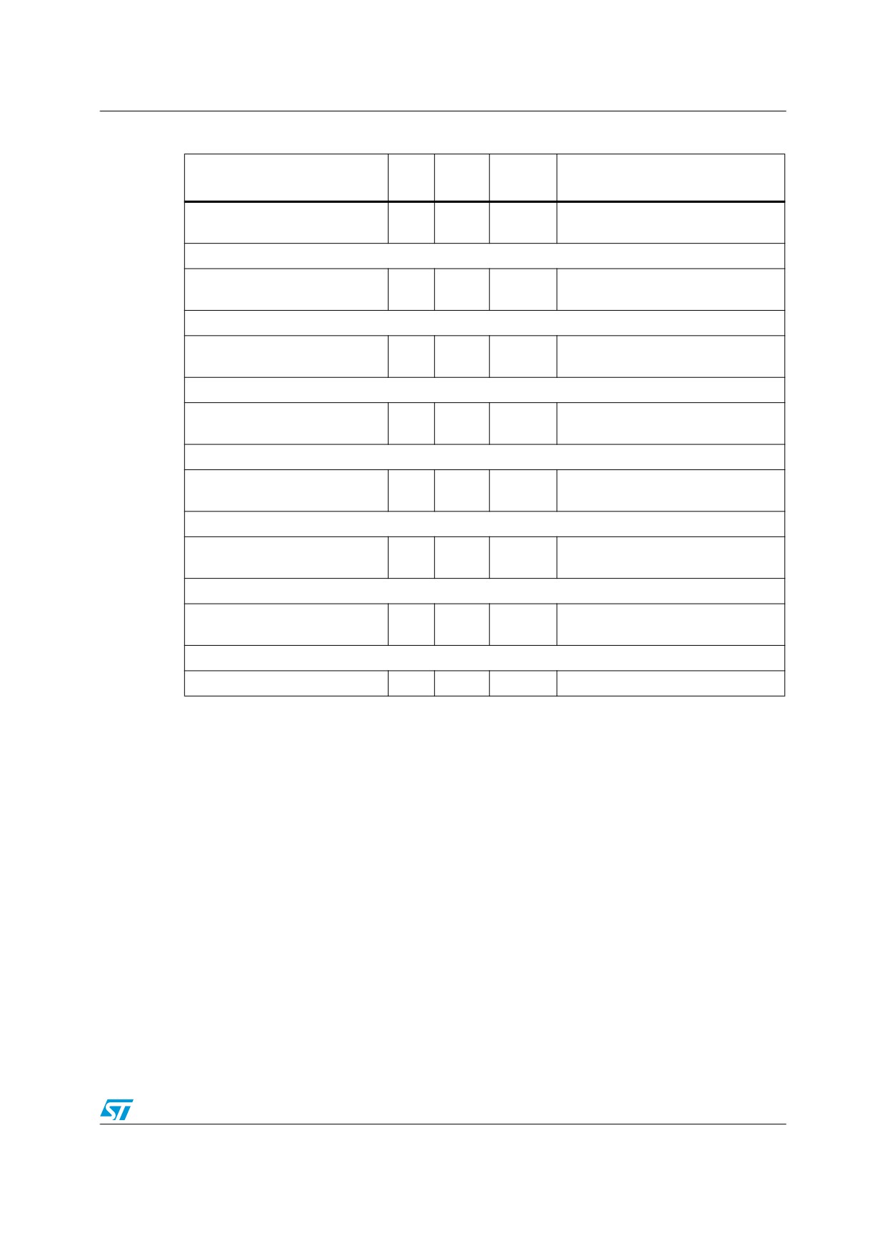
DDR2 SDRAM controller interface description
Table 12. DDR SDRAM configuration parameter register format (continued)
Default
Parameters
Bits
Range
Description
value
PORT_CMD_ERROR_ADDR[31
0x0-
Address of port that caused the
31:0
0x0
:0]
0x1ffffffff
PORT command error. Read-only.
CONF_CTL_24[63:32] Offset: 0x180
DDR2 667:0x00000000
PORT_CMD_ERROR_ADDR[36
0x0-
Address of port that caused the
36:32
0x0
:32]
0x1ffffffff
PORT command error. Read-only
CONF_CTL_25[31:0] Offset: 0x190
DDR2 667:0x00000000
0x0-
Data associated with correctable
ECC_C_DATA[31:0]
31:0
0x0
0x1ffffffff
ECC event. Read-only.
CONF_CTL_25[63:32] Offset: 0x190
DDR2 667:0x00000000
0x0-
Data associated with correctable
ECC_C_DATA[63:32]
63:32
0x0
0x1ffffffff
ECC event. Read-only.
CONF_CTL_26[31:0] Offset: 0x1a0
DDR2 667:0x00000000
0x0-
Data associated with uncorrectable
ECC_U_DATA[31:0]
31:0
0x0
0x1ffffffff
ECC event. Read-only.
CONF_CTL_26[63:32] Offset: 0x1a0
DDR2 667:0x00000000
0x0-
Data associated with uncorrectable
ECC_U_DATA[63:32]
63:32
0x0
0x1ffffffff
ECC event. Read-only.
CONF_CTL_27[63:32] Offset: 0x1b0
DDR2 667:0x00000000
Additional cycles to delay CKE for
CKE_DELAY
2:0
0x0
0x0-0x7
status reporting.
CONF_CTL_28[63:32] Offset: 0x1c0
DDR2 667:0x00000001
UB_DIMM
0:0
0x0
0x0-0x1
Enable unbuffered DIMM.
Note:
1.
CONF_CTL_00 AP
The parameter determines whether the auto pre-charge function is enabled. Once the
function is enabled, memory will close the page, after each write/read instruction. If
mass continuous address operation happens, the parameter will caused the
performance degradation.
2.
CONF_CTL_00 CONCURRENTAP
The parameter determines whether the concurrent auto pre-charge function is enabled.
Most of SDRAM vendors do not support this feature.
3.
CONF_CTL_03 SREFRESH
The parameter is used set the self-refresh style. It must be set 0, when returning from
self-refresh.
4.
CONF_CTL_07 CASLAT_LIN_GATE
The parameter is used to control the data sample of memory controller when read
33/48
DDR2 SDRAM controller interface description
operation returns. In general, It is equal to or less than half period of ACALAT_LIN. The
Value of CASLAT_LIN is twice of the one of CAS.
5.
CONF_CTL_15 DLL_INCREMENT
The parameter should not be set 0.
6.
CONF_CTL_15 DLL_START_POINT
The parameter should not be set 0/1 and should be less than the 1.5 times of
DLL_LOCK_VALUE.
7.
CONF_CTL_28 UB_DIMM
The parameter should be set 1, when unbuffered DIMM(s) are used. It should be set 0,
when the SDRAM(s) are used.
4.5
DDR2 SDRAM sample mode configuration
DDR2 SDRAM controller is integrated in the STLS2F01. And the delay compensation circuit
(using DLL) is used to sample return data of DQS. Since there is the delay of data return
path between the memory controller and SDRAM module, it is necessary to introduce a set
of control signals used to measure the delay.
The control signals of DDR2_GATE_I[3:0] and DDR2_GATE_O[3:0] are used to the delay
measurement. On the PCB, DDR2_GATE_I and DDR2_GAT_O are connected together to
imitate the wiring delay on the PCB. Thus, the accuracy of sampling can be guaranteed.
34/48
Initialization process
5
Initialization process
The initialization of STLS2F01 is divided into core part and interface part.
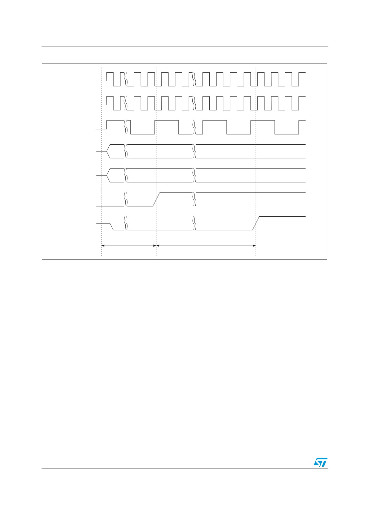
When STLS2F01 PCI interface is configured as main bridge, interface initialization is
finished internally. And PCI_RESETn is output signal. When the processor works as
PCI/PCI-X devices used in other system, PCI_RESETn acts as input to reset the PCI
interface of STLS2F01.
When processor reset signal SYSRESETn is low, related clock, test signals and initial
signals must be valid.
● SYSCLK, MEMCLK, CLKSEL and PCI_CLK must be stable
● Initial signal PCI_CONFIG should set to appropriate value
● TEST_CTRL[7:0] are all high
When SYSRESETn is invalid, the processor internal reset logic begins to work to initialize
the chip. The SYSRESETn should be valid at least one clock cycle to ensure it can be
sampled by reset logic.
The work-mode of PCI bus is decided by main bridge during reset period. As such,
PCI_RESETn output generated by processor when it works as main bridge will be used to
ensure all devices working at the same mode. When not in main bridge mode,
PCI_RESETn input will be used to receive bus configuration.
35/48
Initialization process
Figure 9. Initialization process when in main bridge mode
SYSCLK
MEMCLK
PCI_CLK
PCICONFIG
TESTCTRL
SYSRESETn
PCI_RESETn
1ms
64K SYSCLK
˜
36/48
Electrical characteristics
6
Electrical characteristics
6.1
Absolute maximum rating
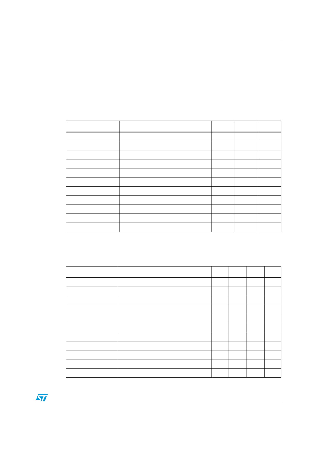
Stresses above the absolute maximum ratings listed in Table 13 may cause permanent
damage to the device. These are stress ratings only and functional operation of the device
at these conditions is not implied. Exposure to maximum rating conditions for extended
period may affect device reliability.
Table 13. Absolute maximum rating.
Parameter
Description
Min
Max
Unit
vdd
CPU core voltage
1.2
1.3
V
vdde1v8
DDR2 voltage
1.7
1.9
V
vdde3v3
IO voltage
3.0
3.6
V
DDR2_VREF
DDR2 voltage reference
0.83
0.97
V
pll_vdd_1
1.0V PLL1 digital voltage
0.9
1.3
V
pll_vdd_0
1.0V PLL0 digital voltage
0.9
1.3
V
pllio_vdde1v8
1.8V PLL IO voltage
1.7
1.9
V
pll_vdde1v8_1
1.8V PLL1 analog voltage
1.7
1.9
V
Pll_vdde1v8_0
1.8V PLL0 analog voltage
1.7
1.9
V
pllio_vdd
1.2V PLL IO voltage
0.9
1.3
V
TS
Storage Temperature
°C
6.2
Recommended operation environment
Table 14. Recommended operating temperature, voltage supply and frequency
Parameter
Description
Min
Typ
Max
Unit
TA
Operating Temperature
0
85
°C
vdd
CPU core voltage
1.25
V
Vdde1v8
DDR2 voltage
1.8
V
vdde3v3
I/O voltage
3.3
V
DDR2_VREF
DDR2 voltage reference
0.9
V
pll_vdd_1
1.0V PLL1 digital voltage
1.2
V
pll_vdd_0
1.0V PLL0 digital voltage
1.2
V
pllio_vdde1v8
1.8V PLL I/O voltage
1.8
V
pll_vdde1v8_1
1.8V PLL1 analog voltage
1.8
V
Pll_vdde1v8_0
1.8V PLL0 analog voltage
1.8
V
pllio_vdd
1.2V PLL I/O voltage
1.2
V
37/48
Electrical characteristics
6.3
DC parameters
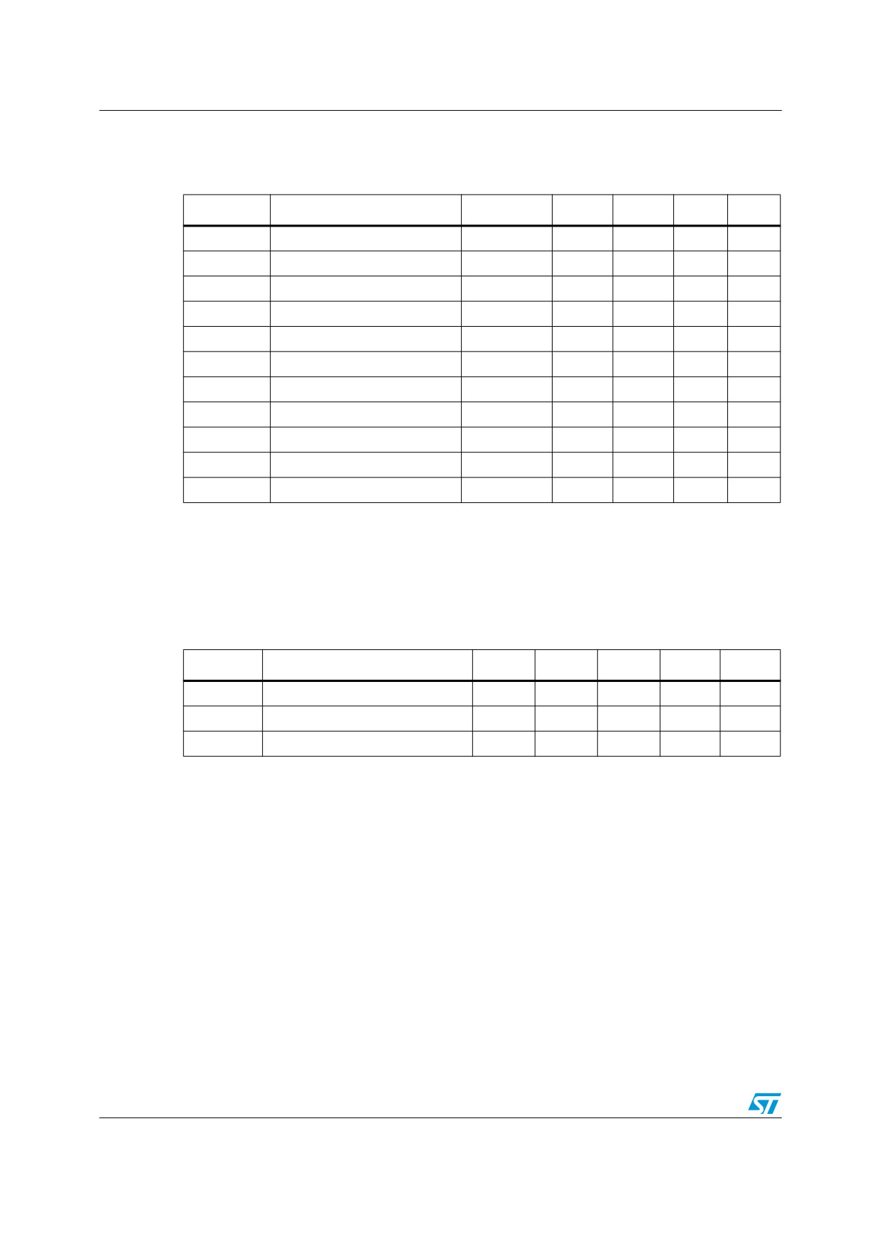
Table 15. DC parameters
Parameter
Description
Min
Typ
Max
Unit
Note
(1)
VIH
Input high level voltage
2
V
(1)
VIL
input low level voltage
0.8
V
(2)
VOH
output high level voltage
vdde3v3-0.3
V
(2)
VOL
output low level voltage
0.3
V
(3)
IIH
input high level leakage current
0.002
0.4
µA
(3)
IIL
input low level leakage current
-67.3
-65
µA
(4)
IOL
output low level current
8
mA
(4)
IOH
output high level current
8
mA
CIN
Input pin capacitor
4.4
7
7.5
pF
COUT
Output pin capacitor
23
25
27
pF
(5)
RPH
Pull-up resistance
32
50
81
KΩ
1. Input pin level (including tri-state pin).
2. Individual output pin (including output state tri-state pin) level.
3. For tri-state input pin (excluding input).
4. Individual output pin (including output state tri-state pin) driving capability.
5. For input pin (excluding tri-state pin).
Table 16. DC parameters (JTAG)
Parameter
Description
Min
Typ
Max
Unit
Note
(1)
CTIN
Test input capacitance
4.4
7
7.5
pF
(2)
CTOUT
Test output capacitance
23
25
27
pF
CTCK
TCK capacitance
4.4
7
7.5
pF
1. For TDI, TMS and TRST in JTAG.
2. For TDO in JTAG.
38/48
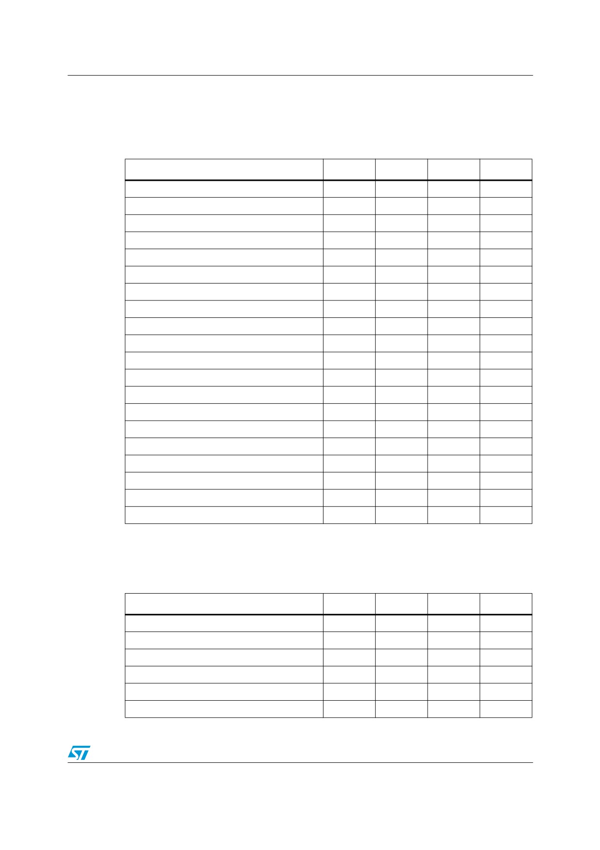
Electrical characteristics
6.4
AC parameters
Table 17. Clock parameters
(Test Conditions: SYSCLK=100 MHz, PCICLK=133 MHz, MEMCLK=333 MHz,
CoreClk=1000 MHz)
Parameter
Min
Typ
Max
Unit
SYSCLK High Level Time
2
5
8
ns
SYSCLK Low Level Time
2
8
ns
SYSCLK Rising Time
1
1
ns
SYSCLK Falling Time
1
1
ns
SYSCLK Cycle Variation
±300
ps
PCI_CLK High Level Time
3
ns
PCI_CLK Low Level Time
3
ns
PCI_CLK Rising Slew
1.5
V/ns
PCI_CLK Falling Slew
1.5
V/ns
PCI_CLK Cycle Variation
±500
ps
MEMCLK High Level Time
1.41
1.59
ns
MEMCLK Low Level Time
1.41
1.59
ns
MEMCLK Rising Slew
1
V/ns
MEMCLK Falling Slew
1
V/ns
MEMCLK Cycle Variation
±225
ps
DQS High Level Time
1.35
1.65
ns
DQS Low Level Time
1.35
1.65
ns
DQS Rising Slew
1
V/ns
DQS Falling Slew
1
V/ns
DQS Cycle Variation
±225
ps
Table 18. Input setup and hold time
(Test Conditions: SYSCLK=100 MHz, PCICLK=133 MHz, MEMCLK=333 MHz,
CoreClk=1000 MHz)
Parameter
Min
Tpy
Max
Unit
PCI_* Signals Setup Time
1.2
ns
PCI_* Signals Hold Time
0.5
ns
LIO_* Signals Setup Time
1.2
ns
LIO_* Signals Hold Time
0.5
ns
DDR2_DQ*/CB* Signals Setup Time
0.1
ns
DDR2_DQ*/CB* Signals Hold Time
0.175
ns
39/48
Electrical characteristics
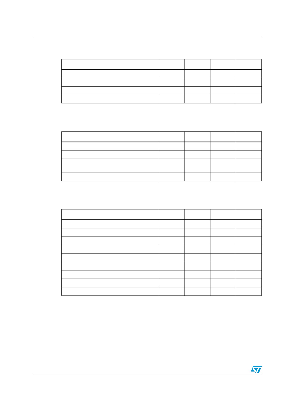
Table 19. Input setup and hold time
(Test Conditions: SYSCLK=100 MHz, PCICLK=66 MHz, CoreClk=1000 MHz)
Parameter
Min
Tpy
Max
Unit
PCI_* Signals Setup Time
3.0
ns
PCI_* Signals Hold Time
0.0
ns
LIO_* Signals Setup Time
3.0
ns
LIO_* Signals Hold Time
0.0
ns
Table 20. Output delay time
(Test Conditions: SYSCLK=100 MHz, PCICLK=133 MHz, CoreClk=1000 MHz)
Parameter
Min
Typ
Max
Unit
PCI_* Signals Effective Delay
0.7
3.8
ns
LIO_* Signals Effective Delay
1.5
6.0
ns
DDDR2_A*/RAS*/CAS*/WE*/CS*/CKE*/ODT*
1.5
ns
Signals Effective Delay
DDR2_DQ*/DQM* Effective Delay
0.75
ns
Table 21. JTAG parameters
(Test Condition: TCK = 100 MHz)
Parameter
Min
Typ
Max
Unit
TCK high level time
2
5
8
ns
TCK low level time
2
8
ns
TCK rising time
1
1
ns
TCK falling time
1
1
ns
TRST pulse width
10
ns
TDI,TMS setup time
3.5
4.4
ns
TDI,TMS hold time
2.5
5.5
ns
TDO output effective delay
1.28
ns
TDO output disable delay
1.28
ns
40/48
Thermal characteristics
7
Thermal characteristics
7.1
Thermal resistivity
Heat spreader optimized with the following assumptions
● Ambient temperature 40 °C
● Package assembled on PCB as per JEDEC EIA/JESD51-9
● Max power 7.45 W
Customer should implement power extraction from the top of the package so that package
case to ambient Rth is below 16 °C/W.
Without air flow, this can be achieved with a 40x40x15 heat spreader or 27x27x25 HS or
35x35x18 HS. This should guarantee 120 °C max junction temperature (low margin).
The preferred configuration is to use a 27x27x10 HS with 0.5m/s air flow. A single fan in PC
case should be enough. In such case, max Junction temp should be around 112 °C.
7.2
Reflow temperature to time curve
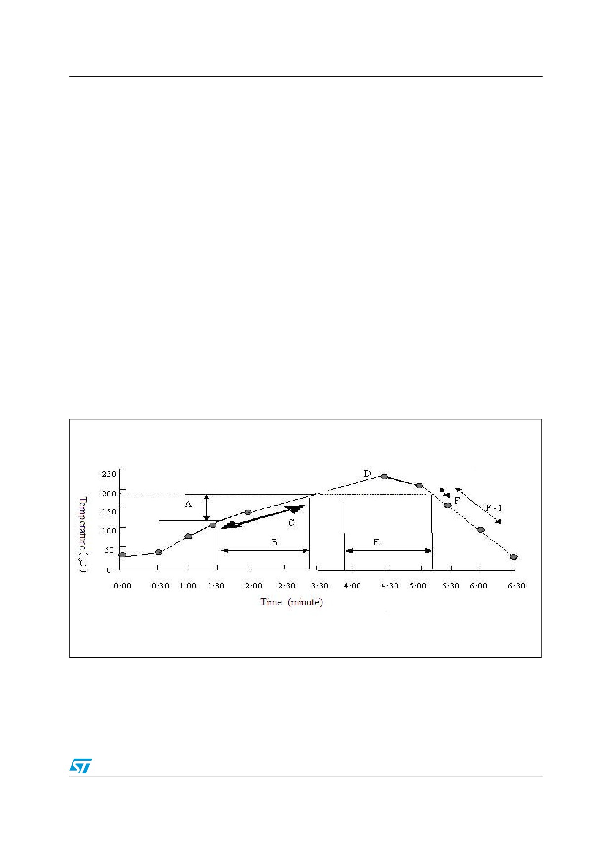
The STLS2F01 processor uses a flip-chip eutectic packaging technology. It can endure
maximum reflow temperature ranging from 235 °C to 245 °C. The reflow temperature curve
and parameters are showed in Figure 10 and Table 22.
Figure 10.
Reflow temperature to time curve
41/48

Thermal characteristics
Table 22. Reflow temperature parameters
Parameter
Value
Unit
A
120 ~ 180
°C
B
90 ~ 120
sec
C
0.3 ~ 2.0
°C/sec
D
235 ~ 245
°C
E
85 ~ 105
sec
F
< 1.2
°C/sec
F-1
< 1.0
°C/sec
42/48
Pin arrangement and package information
8
Pin arrangement and package information
8.1
Pin arrangement
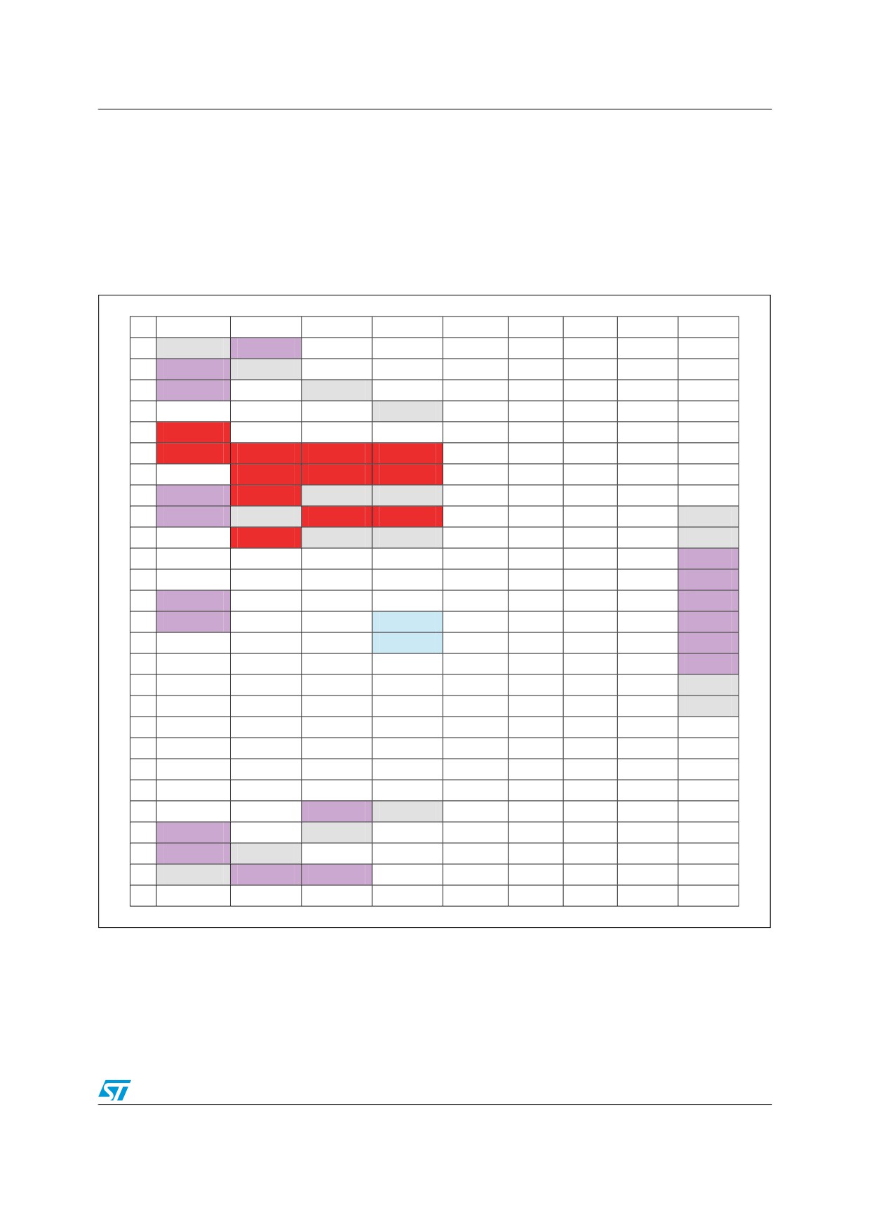
The STLS2F01 processor is packaged in HFCBGA452. The pin arrangement is showed in
Figure 11, and Figure 13,
Figure 11. Pin arrangement (left-hand side)
1
2
3
4
5
6
7
8
9
A
gnde
vdd
TEST_CTRL7
LIO_AD01
LIO_AD04
LIO_AD12
LIO_A3
LIO_A5
LIO_A7
B
vdd
gnde
TEST_CTRL5
TEST_CTRL6
LIO_AD05
LIO_AD08
LIO_A1
LIO_A4
sysclk
C
vdd
TEST_CTRL3
gnde
memclk
SYSRESETN
LIO_AD06
LIO_AD14
LIO_A0
testclk
D
TEST_CTRL0
TEST_CTRL1
TEST_CTRL2
gnde
pllclock1
LIO_AD02
LIO_AD10
LIO_AD09
pllclock0
E
pll_vdd_1
gpio0
gpio2
gpio3
F
pllio_vdde1v8
pll_gnd_1
pll_vdde1v8_1
pll_gnde_1
G
gpio1
pllio_gnd
pllio_vdd
pllio_gnde
H
vdd
pll_gnde_0
gnde
gnde
9
J
vdd
gnde
pll_gnd_0
pll_vdde1v8_0
J
gnde
K
CLKSEL7
pll_vdd_0
gnde
gnde
K
gnde
L
CLKSEL6
CLKSEL5
CLKSEL8
CLKSEL9
L
vdd
M
CLKSEL3
CLKSEL4
CLKSEL0
CLKSEL2
M
vdd
N
vdd
CLKSEL1
PCI_CONFIG7
PCI_CONFIG6
N
vdd
P
vdd
PCI_CONFIG5
PCI_CONFIG4
vdde3v3
P
vdd
R
PCI_CONFIG3
PCI_CONFIG0
PCI_CONFIG1
vdde3v3
R
vdd
T
PCI_CONFIG2
PCI_IDSEL
PCI_AD00
PCI_AD02
T
vdd
U
PCI_AD01
PCI_AD03
PCI_AD05
PCI_AD04
U
gnde
V
PCI_CBEn0
PCI_AD06
PCI_AD07
PCI_AD08
V
gnde
W
PCI_AD10
PCI_AD09
PCI_AD12
PCI_AD14
9
Y
GND
PCI_AD11
PCI_AD13
PCI_CBEn1
AA
PCI_AD15
PCI_PAR
PCI_SERR
PCI_FRAMEn
AB
PCI_PERR
PCI_STOPn
PCI_IRDYn
VDD
AC
PCI_TRDYn
PCI_DEVSELn
vdd
gnde
PCI_AD19
PCI_AD22
PCI_AD28
PCI_AD30
PCI_GNTn5
AD
vdd
PCI_CBEn2
gnde
PCI_AD17
PCI_AD23
PCI_AD24
PCI_AD27
PCI_GNTn6
PCI_REQn5
AE
vdd
gnde
PCI_AD16
PCI_AD18
PCI_AD21
PCI_AD26
PCI_AD31
PCI_REQn6
PCI_GNTn3
AF
gnde
vdd
vdd
PCI_AD20
PCI_CBEn3
PCI_AD25
PCI_AD29
PCI_REQn4
PCI_GNTn4
1
2
3
4
5
6
7
8
9
43/48
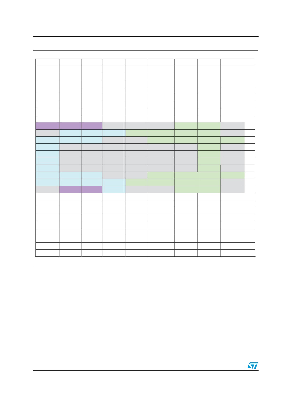
Pin arrangement and package information
Figure 12.
Pin arrangement (middle)
10
11
12
13
14
15
16
17
18
TEST_CTRL4
LIO_AD07
LIO_A2
LIO_ADLOCK
DDR2_VREF
DDR2_DQSn0
DDR2_DQ03
DDR2_DQ12
DDR2_DQM1
A
LIO_AD00
LIO_AD15
LIO_A6
LIO_DIR
DDR2_DQ00
DDR2_DQSp0
DDR2_DQ02
DDR2_DQ09
DDR2_DQSp1
B
LIO_AD03
LIO_AD13
LIO_RDn
LIO_DEN
DDR2_DQ04
DDR2_DQ05
DDR2_DQ06
DDR2_DQ08
DDR2_DQSn1
C
LIO_AD11
LIO_CSn
LIO_WRn
LIO_ROMCSn
DDR2_DQ01
DDR2_DQM0
DDR2_DQ07
DDR2_DQ13
DDR2_GATEI0
D
E
F
G
10
11
12
13
14
15
16
17
18
H
vdd
vdd
vdd
gnde
gnde
gnde
vdde1v8
vdde1v8
gnde
J
gnde
vdde3v3
vdde3v3
vdde3v3
vdde1v8
vdde1v8
vdde1v8
vdde1v8
gnde
K
vdde3v3
vdde3v3
vdde3v3
gnd
gnd
vdde1v8
vdde1v8
vdde1v8
vdde1v8
L
vdde3v3
gnd
gnd
gnd
gnd
gnd
gnd
vdde1v8
gnde
M
vdde3v3
gnd
gnd
gnd
gnd
gnd
gnd
vdde1v8
gnde
N
vdde3v3
gnd
gnd
gnd
gnd
gnd
gnd
vdde1v8
gnde
P
vdde3v3
gnd
gnd
gnd
gnd
gnd
gnd
vdde1v8
gnde
R
vdde3v3
vdde3v3
vdde3v3
gnd
gnd
vdde1v8
vdde1v8
vdde1v8
vdde1v8
T
vdde3v3
vdde3v3
vdde3v3
vdde3v3
vdde1v8
vdde1v8
vdde1v8
vdde1v8
gnde
U
gnde
vdd
vdd
vdde3v3
gnde
gnde
vdde1v8
vdde1v8
gnde
V
10
11
12
13
14
15
16
17
18
W
Y
AA
AB
PCI_REQn3
PCI_GNTn1
PCI_IRQnA
INTN1
tck
comp1v8_resistor
DDR2_SCSn1
DDR2_A00
DDR2_ODT0
AC
PCI_REQn2
PCI_REQn0
PCI_IRQnC
INTN2
tdo
PCI_CLK
DDR2_ODT3
DDR2_SCSn3
DDR2_ODT2
AD
PCI_GNTn2
PCI_GNTn0
PCI_IRQnB
INTN3
trst
tms
DDR2_ODT1
DDR2_A01
DDR2_CASn
AE
PCI_REQn1
PCI_RESETn
PCI_IRQnD
NMIN
INTN0
tdi
comp1v8_gnd
DDR2_A02
DDR2_A13
AF
10
11
12
13
14
15
16
17
18
44/48
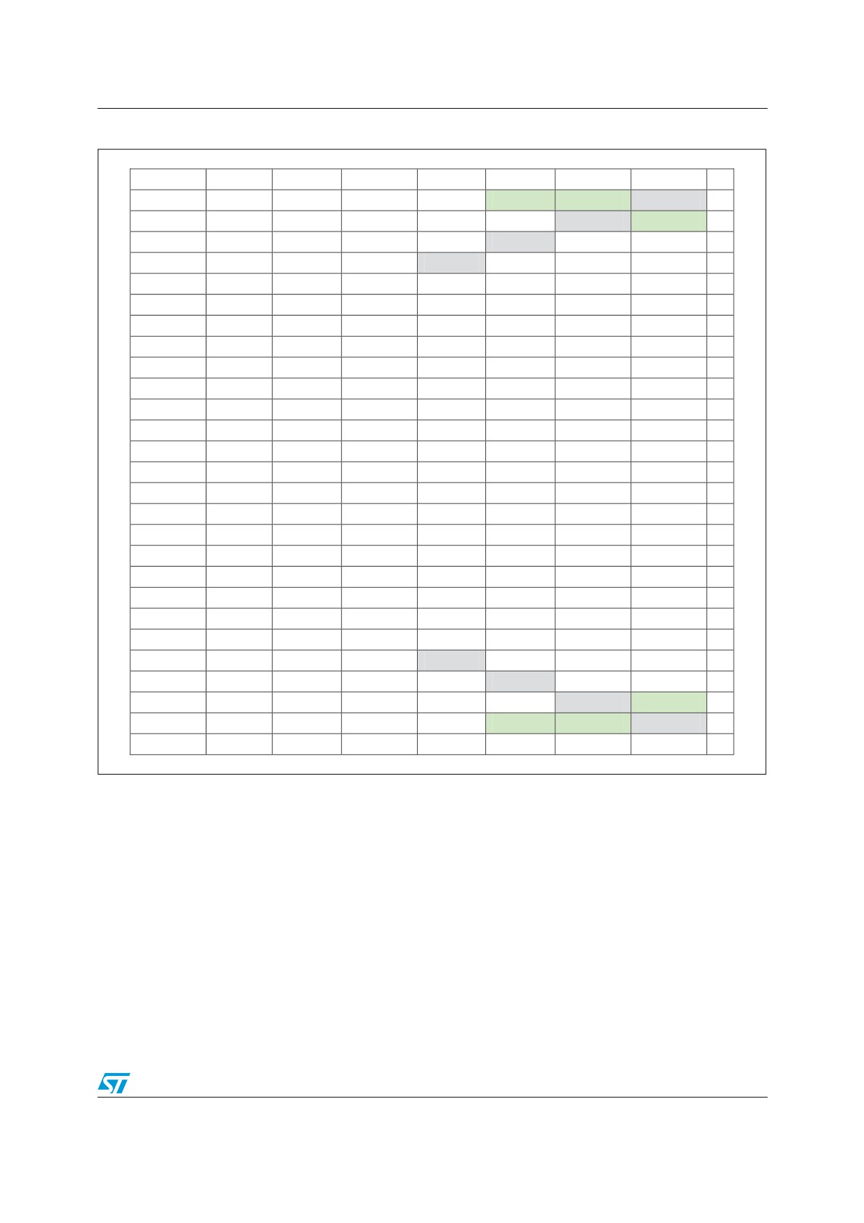
Pin arrangement and package information
Figure 13. Pin arrangement (right-hand side)
19
20
21
22
23
24
25
26
DDR2_GATEO0
DDR2_DQM2
DDR2_DQ20
DDR2_DQ22
DDR2_CKE3
vdde1v8
vdde1v8
gnde
A
DDR2_DQ14
DDR2_DQ16
DDR2_DQ17
DDR2_DQ23
DDR2_CKn4
DDR2_CKE1
gnde
vdde1v8
B
DDR2_DQ15
DDR2_DQ10
DDR2_DQSp2
DDR2_DQ18
DDR2_CKp4
gnde
DDR2_CKE2
DDR2_A12
C
DDR2_DQ11
DDR2_DQ21
DDR2_DQSn2
DDR2_DQ19
gnde
DDR2_CKn1
DDR2_CKp1
DDR2_BA2
D
DDR2_A14
DDR2_A07
DDR2_A11
DDR2_A06
E
DDR2_A08
DDR2_CKE0
DDR2_A05
DDR2_A04
F
DDR2_A09
DDR2_A03
DDR2_DQ29
DDR2_DQ28
G
DDR2_DQM3
DDR2_DQ25
DDR2_DQ24
DDR2_DQ31
H
J
DDR2_DQ30
DDR2_DQ36
DDR2_DQSn3
DDR2_DQSp3
J
K
DDR2_DQ27
DDR2_DQ26
DDR2_GATEO1
DDR2_GATEI1
K
L
DDR2_DQ37
DDR2_DQ33
DDR2_DQ32
DDR2_DQM4
L
M
DDR2_DQ39
DDR2_DQ38
DDR2_DQSn4
DDR2_DQSp4
M
N
DDR2_DQ34
DDR2_DQ35
DDR2_CKp3
DDR2_CKn3
N
P
DDR2_BA1
DDR2_A10
DDR2_CKn0
DDR2_CKp0
P
R
DDR2_SCSn2
DDR2_SCSn0
DDR2_BA0
DDR2_RASn
R
T
DDR2_DQ44
DDR2_DQ40
DDR2_DQ45
DDR2_DQ41
T
U
DDR2_DQ43
DDR2_DQSn5
DDR2_DQSp5
DDR2_DQM5
U
V
DDR2_DQ48
DDR2_DQ47
DDR2_DQ42
DDR2_DQ46
V
DDR2_DQ52
DDR2_DQ49
DDR2_GATEI2
DDR2_GATEO2
W
DDR2_DQ55
DDR2_DQ51
DDR2_DQSp6
DDR2_DQSn6
Y
DDR2_DQM6
DDR2_DQ53
DDR2_DQ54
DDR2_DQ50
AA
DDR2_DQ61
DDR2_DQ60
DDR2_DQM7
DDR2_DQ56
AB
DDR2_WEn
DDR2_CB2
DDR2_DQM8
DDR2_GATEI3
gnde
DDR2_DQSp7
DDR2_DQSn7
DDR2_DQ57
AC
DDR2_CKp2
DDR2_CB3
DDR2_CB6
DDR2_GATEO3
DDR2_DQ59
gnde
DDR2_DQ62
DDR2_DQ58
AD
DDR2_CKn2
DDR2_CB7
DDR2_DQSp8
DDR2_CB5
DDR2_CB4
DDR2_DQ63
gnde
vdde1v8
AE
DDR2_CKn5
DDR2_CKp5
DDR2_DQSn8
DDR2_CB1
DDR2_CB0
vdde1v8
vdde1v8
gnde
AF
19
20
21
22
23
24
25
26
45/48
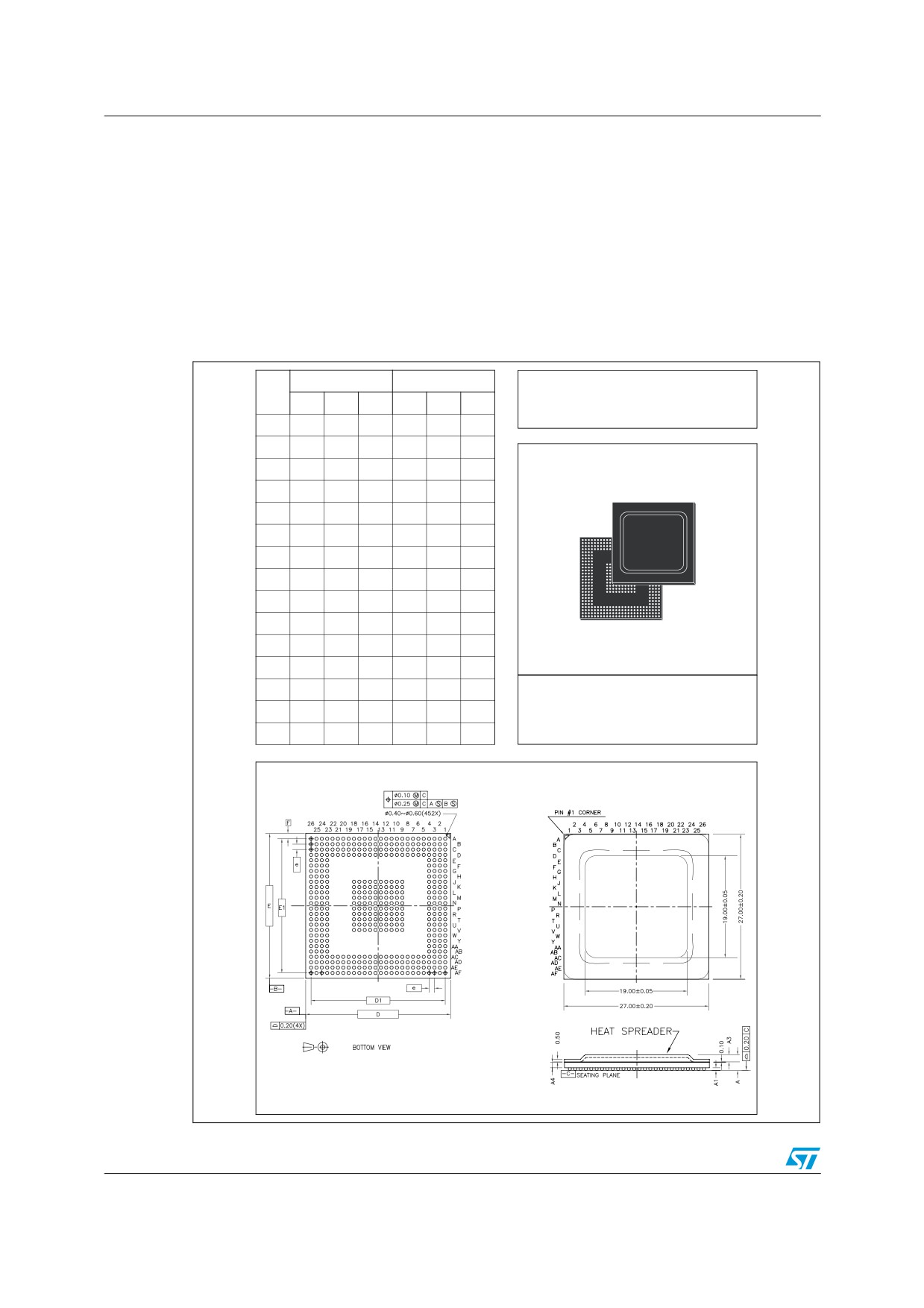
Package information
9
Package information
In order to meet environmental requirements, ST offers these devices in ECOPACK®
packages. These packages have a Lead-free second level interconnect. The category of
second Level Interconnect is marked on the package and on the inner box label, in
compliance with JEDEC Standard JESD97. The maximum ratings related to soldering
conditions are also marked on the inner box label.
ECOPACK is an ST trademark. ECOPACK specifications are available at: www.st.com.
Figure 14. HFCBGA452 mechanical data & package dimensions
mm
inch
DIM.
OUTLINE AND
MIN.
TYP.
MAX.
MIN.
TYP.
MAX.
MECHANICAL DATA
A
3.150
0.1240
A1
0.250
0.0098
A3
1.300
0.0512
A4
1.000
0.0394
b
0.450
0.500
0.550
0.0177
0.0197
0.0217
D
26.800
27.000
27.200
1.0551
1.0630
1.0709
D1
25.000
0.9843
E
26.800
27.000
27.200
1.0551
1.0630
1.0709
E1
25.000
0.9843
e
1.000
0.0394
F
1.000
0.0394
aaa
0.200
0.0079
ddd
0.200
0.0079
HFCBGA452 (27x27x2.9mm)
eee
0.250
0.0098
Heat Spreader Flip Chip Ball Grid Array
fff
0.100
0.0039
8061758 A
46/48
Revision history
10
Revision history
Table 23. Document revision history
Date
Revision
Changes
30-May-2008
1
Initial relase.
47/48
Please Read Carefully:
Information in this document is provided solely in connection with ST products. STMicroelectronics NV and its subsidiaries (“ST”) reserve the
right to make changes, corrections, modifications or improvements, to this document, and the products and services described herein at any
time, without notice.
All ST products are sold pursuant to ST’s terms and conditions of sale.
Purchasers are solely responsible for the choice, selection and use of the ST products and services described herein, and ST assumes no
liability whatsoever relating to the choice, selection or use of the ST products and services described herein.
No license, express or implied, by estoppel or otherwise, to any intellectual property rights is granted under this document. If any part of this
document refers to any third party products or services it shall not be deemed a license grant by ST for the use of such third party products
or services, or any intellectual property contained therein or considered as a warranty covering the use in any manner whatsoever of such
third party products or services or any intellectual property contained therein.
UNLESS OTHERWISE SET FORTH IN ST’S TERMS AND CONDITIONS OF SALE ST DISCLAIMS ANY EXPRESS OR IMPLIED
WARRANTY WITH RESPECT TO THE USE AND/OR SALE OF ST PRODUCTS INCLUDING WITHOUT LIMITATION IMPLIED
WARRANTIES OF MERCHANTABILITY, FITNESS FOR A PARTICULAR PURPOSE (AND THEIR EQUIVALENTS UNDER THE LAWS
OF ANY JURISDICTION), OR INFRINGEMENT OF ANY PATENT, COPYRIGHT OR OTHER INTELLECTUAL PROPERTY RIGHT.
UNLESS EXPRESSLY APPROVED IN WRITING BY AN AUTHORIZED ST REPRESENTATIVE, ST PRODUCTS ARE NOT
RECOMMENDED, AUTHORIZED OR WARRANTED FOR USE IN MILITARY, AIR CRAFT, SPACE, LIFE SAVING, OR LIFE SUSTAINING
APPLICATIONS, NOR IN PRODUCTS OR SYSTEMS WHERE FAILURE OR MALFUNCTION MAY RESULT IN PERSONAL INJURY,
DEATH, OR SEVERE PROPERTY OR ENVIRONMENTAL DAMAGE. ST PRODUCTS WHICH ARE NOT SPECIFIED AS "AUTOMOTIVE
GRADE" MAY ONLY BE USED IN AUTOMOTIVE APPLICATIONS AT USER’S OWN RISK.
Resale of ST products with provisions different from the statements and/or technical features set forth in this document shall immediately void
any warranty granted by ST for the ST product or service described herein and shall not create or extend in any manner whatsoever, any
liability of ST.
ST and the ST logo are trademarks or registered trademarks of ST in various countries.
Information in this document supersedes and replaces all information previously supplied.
The ST logo is a registered trademark of STMicroelectronics. All other names are the property of their respective owners.
STMicroelectronics group of companies
Australia - Belgium - Brazil - Canada - China - Czech Republic - Finland - France - Germany - Hong Kong - India - Israel - Italy - Japan -
Malaysia - Malta - Morocco - Singapore - Spain - Sweden - Switzerland - United Kingdom - United States of America
48/48